
G -LINK
GLT41316
64K X 16 CMOS DYNAMIC RAM WITH FAST PAGE MODE
June 1998 (Rev 2)
G-Link Technology Corporation
2701Northwestern Parkway
Santa Clara, CA 95051, U.S.A.
G-Link Technology Corporation, Taiwan
2F, No.12, R&D Rd. II, Science-Based Industrial Park,
Hsin Chu, Taiwan, R.O.C.
- 1 -
Features :
Description :
65,536 words by 16 bits organization.
Fast access time and cycle time.
Dual WE Input.
Low power dissipation.
Read-Modify-Write, RAS -Only Refresh,
CAS -Before- RAS Refresh, Hidden
Refresh and Test Mode Capability.
256 refresh cycles per 4ms.
Available in 40-pin 400 mil SOJ,and 40/44
pin TSOP (II).
Single 5.0V
�
10% Power Supply.
All inputs and Outputs are TTL
compatible.
Fast Page Mode operation.
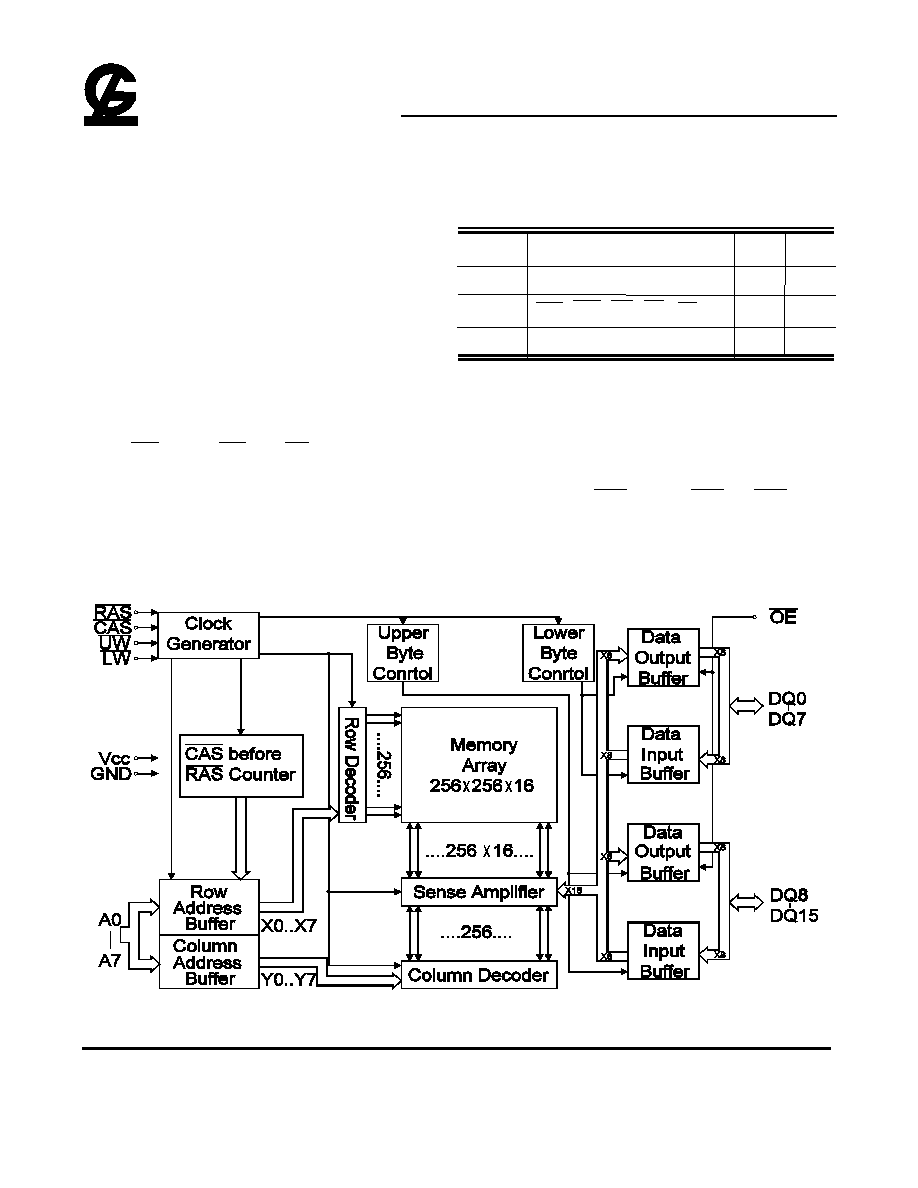
The GLT41316 is a 65,536 x 16 bit high-
performance CMOS dynamic random access
memory. The GLT41316 offers Fast Page
mode ,and has both BYTE WRITE and
WORD WRITE access cycles via two WE
pins. The GLT41316 has symmetric address
and accepts 256-cycle refresh in 4ms
interval.
All inputs are TTL compatible. Fast
Page Mode operation allows random access
up to 256x16 bits, within a page, with cycle
times as short as 18ns.
The GLT41316 is best suited for
graphics, and DSP applications requiring
high performance memories.
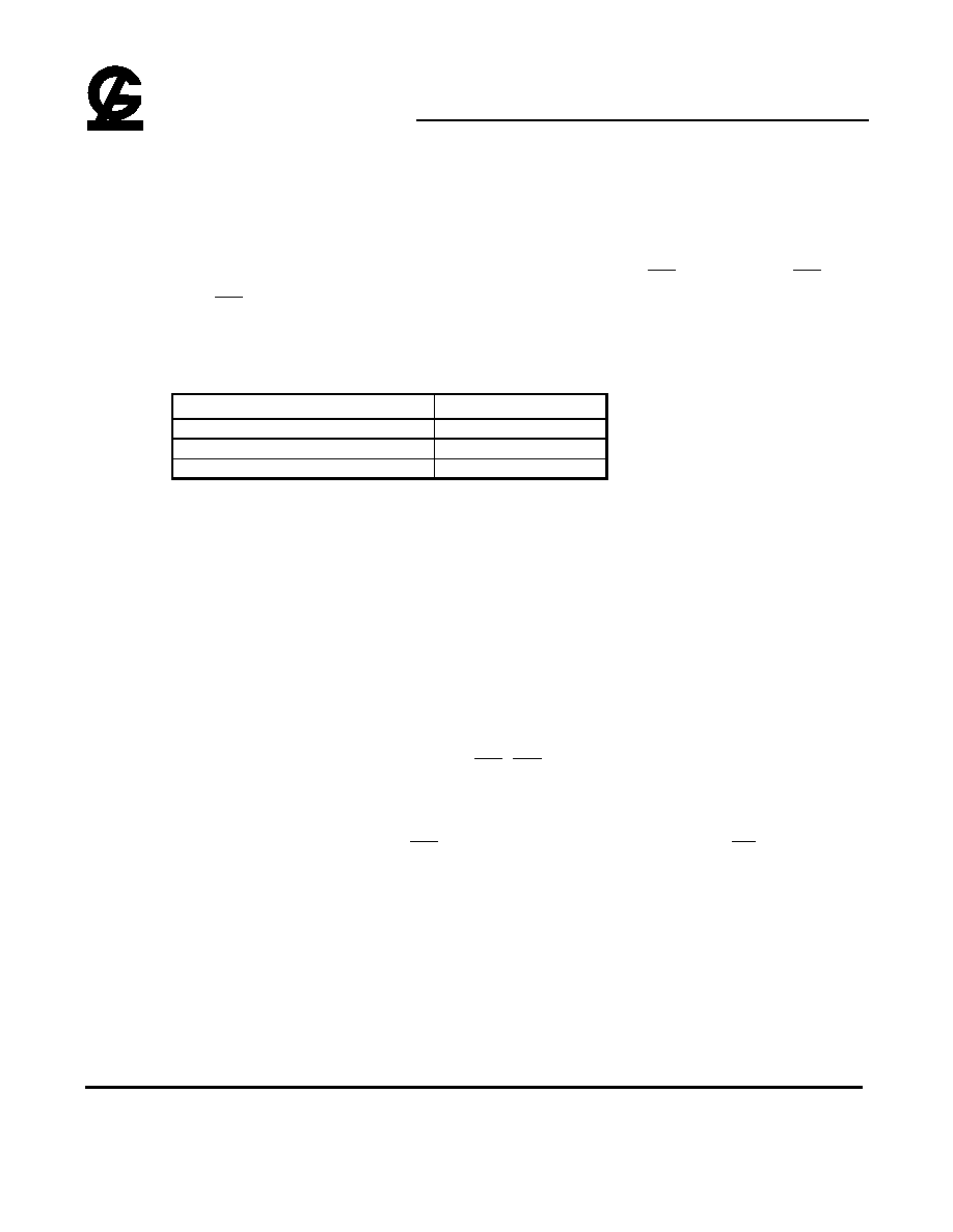
HIGH PERFORMANCE
30
35
40
45
Max. RAS Access Time, (t
RAC
)
30 ns
35 ns
40 ns
45 ns
Max. Column Address Access Time, (t
AA
)
15 ns
18 ns
20 ns
22 ns
Min. Fast Page Mode Cycle Time, (t
PC
)
18 ns
21 ns
23 ns
25 ns
Min. Read/Write Cycle Time, (t
RC
)
65 ns
70 ns
75 ns
80 ns
Max. CAS Access Time (t
CAC
)
10 ns
11 ns
12 ns
12 ns

G -LINK
GLT41316
64K X 16 CMOS DYNAMIC RAM WITH FAST PAGE MODE
June 1998 (Rev 2)
G-Link Technology Corporation
2701Northwestern Parkway
Santa Clara, CA 95051, U.S.A.
G-Link Technology Corporation, Taiwan
2F, No.12, R&D Rd. II, Science-Based Industrial Park,
Hsin Chu, Taiwan, R.O.C.
- 2 -
Pin Configuration :
Pin Descriptions:
Name
Function
A
0
- A
7
Address Inputs
RAS
Row Address Strobe
CAS
Column Address Strobe
UW
Read / Upper Byte Write Enable
LW
Read / Lower Byte Write Enable
OE
Output Enable
DQ
0
- DQ
15
Data Inputs / Outputs
V
CC
+5V Power Supply
V
SS
Ground
NC
No Connection
GLT41316
SOJ Top View
TSOP(Type II)
Top View
G -LINK
GLT41316
64K X 16 CMOS DYNAMIC RAM WITH FAST PAGE MODE
June 1998 (Rev 2)
G-Link Technology Corporation
2701Northwestern Parkway
Santa Clara, CA 95051, U.S.A.
G-Link Technology Corporation, Taiwan
2F, No.12, R&D Rd. II, Science-Based Industrial Park,
Hsin Chu, Taiwan, R.O.C.
- 3 -
Absolute Maximum Ratings*
Capacitance*
T
A
=25
�
C, V
CC
=5V
�
10%, V
SS
=0V
Operating Temperature, T
A
(ambient)
.......................................-0
�
C to +70
�
C
Storage Temperature(plastic)....-55
�
C to +150
�
C
Voltage Relative to V
SS
...............-1.0V to + 7.0V
Short Circuit Output Current......................50mA
Power Dissipation......................................1.0W
Symbol
C
IN1
C
IN2
C
OUT
Parameter
Address Input
RAS
,
CAS
,
UW
,
LW
,
OE
Data Input/Output
Max.
5
7
7
Unit
pF
pF
pF
*Note: Operation above Absolute Maximum Ratings
can adversely affect device reliability.
*Note: Capacitance is sampled and not 100% tested
Electrical Specifications
l
WE means UW and LW .
l
All voltages are referenced to GND.
l
After power up, wait more than 100
�
s and then, execute eight CAS -before- RAS or RAS -only
refresh cycles as dummy cycles to initialize internal circuit.
Block Diagram :
G -LINK
GLT41316
64K X 16 CMOS DYNAMIC RAM WITH FAST PAGE MODE
June 1998 (Rev 2)
G-Link Technology Corporation
2701Northwestern Parkway
Santa Clara, CA 95051, U.S.A.
G-Link Technology Corporation, Taiwan
2F, No.12, R&D Rd. II, Science-Based Industrial Park,
Hsin Chu, Taiwan, R.O.C.
- 4 -
Truth Table: GLT41316
Function
RAS
CAS
UW
LW
OE
ADDRESS
DQs
Note
s
Standby
H
H
X
X
X
X
High-Z
Read: Word
L
L
H
H
L
ROW/COL Data Out
Write: Word(Early Write)
L
L
L
L
X
ROW/COL Data-In
Write: Lower Byte (Early)
L
L
H
L
X
ROW/COL Lower Byte,Data-In
Upper Byte,High-Z
Write: Upper Byte (Early)
L
L
L
H
X
ROW/COL Lower Byte,High-Z
Upper Byte,Data-In
Read Write
L
L
H
L
H
L
L
H
ROW/COL Data-Out,Data-In
1,2
Fast-Page-
Mode Read
1st Cycle
2nd Cycle
L
L
H
L
H
L
H
H
H
L
L
ROW/COL
COL
Data-Out
Data-Out
1
1
Fast-Page-
Mode Write
1st Cycle
2nd Cycle
L
L
H
L
H
L
L
L
L
L
X
X
ROW/COL
COL
Data-In
Data-In
2
2
Fast-Page-
Mode Read-
Write
1st Cycle
2nd Cycle
L
L
H
L
H
L
H
L
H
L
H
L
H
L
L
H
L
H
ROW/COL
COL
Data-Out,Data-In
Data-Out,Data-In
1,2
1,2
Hidden
Refresh
Read
Write
L
H
L
L
H
L
L
L
H
L
H
L
L
X
ROW/COL
ROW/COL
Data-Out
Data-In
1
2,3
RAS -Only Refresh
L
H
X
X
X
ROW
High-Z
CBR Refresh
H
L
L
X
X
X
High-Z
Notes:
1. These READ cycles are always WORD READ cycles .
2. These WRITE cycles may also be BYTE READ cycles (either UW or LW active).
3. EARLY WRITE only.
G -LINK
GLT41316
64K X 16 CMOS DYNAMIC RAM WITH FAST PAGE MODE
June 1998 (Rev 2)
G-Link Technology Corporation
2701Northwestern Parkway
Santa Clara, CA 95051, U.S.A.
G-Link Technology Corporation, Taiwan
2F, No.12, R&D Rd. II, Science-Based Industrial Park,
Hsin Chu, Taiwan, R.O.C.
- 5 -
DC and Operating Characteristics (1-2)
T
A
= 0
�
C to 70
�
C, V
CC
=5V
�
10%, V
SS
=0V, unless otherwise specified.
Sym.
Parameter
Test Conditions
Access
Time
Min.
Typ
Max. Unit Notes
I
LI
Input Leakage Current
(any input pin)
0V
V
IN
5.5V
(All other pins not under
test=0V)
-10
+10
�
A
I
LO
Output Leakage Current
(for High-Z State)
0V
V
out
5.5V
Output is disabled (Hiz)
-10
+10
�
A
I
CC1
Operating Current,
Random READ/WRITE
t
RC
= t
RC
(min.)
t
RAC
= 30ns
t
RAC
= 35ns
t
RAC
= 40ns
t
RAC
= 45ns
180
170
160
150
mA
1,2
I
CC2
Standby Current,(TTL)
RAS
,
CAS
at V
IH
other inputs
V
SS
4
mA
I
CC3
Refresh Current,
RAS-Only
RAS
cycling,
CAS
at
V
IH
t
RC
= t
RC
(min.)
t
RAC
= 30ns
t
RAC
= 35ns
t
RAC
= 40ns
t
RAC
= 45ns
180
170
160
150
mA
2
I
CC4
Operating Current,
EDO Page Mode
RAS
at V
IL
,
CAS
,
address cycling: t
PC
=
t
PC
(min.)
t
RAC
= 30ns
t
RAC
= 35ns
t
RAC
= 40ns
t
RAC
= 45ns
180
170
160
150
mA
1,2
I
CC5
Refresh Current,
CAS Before RAS
RAS
,
CAS
,
address cycling:
t
RC
= t
RC
(min.)
t
RAC
= 30ns
t
RAC
= 35ns
t
RAC
= 40ns
t
RAC
= 45ns
180
170
160
150
mA
1
I
CC6
Standby Current, (CMOS)
RAS
V
CC
-0.2V,
CAS
V
CC
-0.2V,
All other inputs
V
SS
2
mA
V
IL
Input Low Voltage
-1
+0.8
V
3
V
IH
Input High Voltage
2.4
V
CC
+1
V
3
V
OL
Output Low Voltage
I
OL
= 4.2mA
0.4
V
V
OH
Output High Voltage
I
OH
= -5mA
2.4
V
Notes:
1.
I
CC
is dependent on output loading when the device output is selected. Specified I
CC(max.)
is measured with the
output open.
2. I
CC
is dependent upon the number of address transitions specified I
CC(max.)
is measured with a maximum of
one transition per address cycle in random Read/Write and Fast Page Mode.
3. Specified V
IL(min.)
is steady state operation. During transitions V
IL(min.)
may undershoot to -1.0V for a period not
to exceed 20ns. All AC parameters are measured with V
IL(min.)
V
SS
and V
IH(max.)
V
CC
.
G -LINK
GLT41316
64K X 16 CMOS DYNAMIC RAM WITH FAST PAGE MODE
June 1998 (Rev 2)
G-Link Technology Corporation
2701Northwestern Parkway
Santa Clara, CA 95051, U.S.A.
G-Link Technology Corporation, Taiwan
2F, No.12, R&D Rd. II, Science-Based Industrial Park,
Hsin Chu, Taiwan, R.O.C.
- 6 -
AC Characteristics (0
�
�
C
T
A
70
�
�
C, See note 1,2)
Test condition:V
CC
=5.0V
�
10%, V
IH
/V
IL
=2.4V/0.8V,V
OH
/V
OL
=2.4V/0.4V
Parameter
t
RAC
= 30 ns t
RAC
= 35 ns t
RAC
= 40 ns t
RAC
= 45 ns
Symbo
l
MIN. MAX. MIN. MAX. MIN. MAX. MIN. MAX. Unit Notes
Read/Write Cycle Time
t
RC
65
-
70
-
75
-
80
-
ns
Read Midify Write Cycle Time
t
RWC
80
-
99
-
105
-
110
-
ns
Access Time from RAS
t
RAC
-
30
-
35
-
40
-
45
ns
3,4
Access Time from CAS
t
CAC
-
10
-
11
-
12
-
12
ns
3,4
Access Time from Column Address
t
AA
-
15
-
18
-
20
-
22
ns
3,4
CAS to Output in Low-Z
t
CLZ
0
0
-
0
-
0
-
ns
3
Output Buffer Turn-off Delay from CAS
t
OFF
3
8
3
8
3
8
3
8
ns
7
Transition Time(Rise and Fall)
t
T
3
50
3
50
3
50
3
50
ns
2
RAS Precharge Time
t
RP
25
-
25
-
25
-
25
-
ns
RAS Pulse Width
t
RAS
30
100k
35
100k
40
100K
45
100K
ns
RAS Hold Time
t
RSH
10
-
12
-
12
-
13
-
ns
CAS Hold Time
t
CSH
30
-
36
-
40
-
46
-
ns
CAS Pulse Width
t
CAS
10
10000
12
10000
12
10000
13
10000 ns
RAS to CAS Delay Time
t
RCD
13
20
17
24
18
28
18
33
ns
4
RAS to Column Address Delay Time
t
RAD
10
15
12
17
13
20
13
23
ns
4
CAS to RAS Precharge Time
t
CRP
5
-
5
-
5
-
5
-
ns
8
Row Address Setup Time
t
ASR
0
-
0
-
0
-
0
-
ns
Row Address Hold Time
t
RAH
7
-
7
-
8
-
8
-
ns
Column Address Setup Time
t
ASC
0
-
0
-
0
-
0
-
ns
Column Address Hold Time
t
CAH
6
-
6
-
6
-
6
-
ns
Column Address Hold Time Referenced
to RAS
t
AR
26
-
30
-
34
-
39
-
ns
Column Address Lead Time Referenced
to RAS
t
RAL
15
-
18
-
20
-
23
-
ns
Read Command Setup Time
t
RCS
0
-
0
-
0
-
0
-
ns
Read Command Hold Time Referenced
to RAS
t
RRH
0
-
0
-
0
-
0
-
ns
9
Read Command Hold Time Referenced
to CAS
t
RCH
0
-
0
-
0
-
0
-
ns
9
WE Hold Time Referenced to CAS
t
WCH
6
-
6
-
6
-
6
-
ns
10
Write Command Hold Time Referenced
to RAS
t
WCR
26
-
30
-
34
-
39
-
ns
5
WE Pulse Width
t
WP
6
-
6
-
6
-
6
-
ns
10

G -LINK
GLT41316
64K X 16 CMOS DYNAMIC RAM WITH FAST PAGE MODE
June 1998 (Rev 2)
G-Link Technology Corporation
2701Northwestern Parkway
Santa Clara, CA 95051, U.S.A.
G-Link Technology Corporation, Taiwan
2F, No.12, R&D Rd. II, Science-Based Industrial Park,
Hsin Chu, Taiwan, R.O.C.
- 7 -
Parameter
t
RAC
= 30 ns t
RAC
= 35 ns t
RAC
= 40 ns t
RAC
= 45 ns
Symbo
l
MIN. MAX. MIN. MAX. MIN. MAX. MIN. MAX. Unit Notes
WE Lead Time Referenced to RAS
t
RWL
10
-
11
-
12
-
12
-
ns
WE Lead Time Referenced to CAS
t
CWL
10
-
11
-
12
-
12
-
ns
Data-In Setup Time
t
DS
0
-
0
-
0
-
0
-
ns
11
Data-In Hold Time
t
DH
7
-
7
-
8
-
8
-
ns
11
Data Hold Time Referenced to RAS
t
DHR
27
-
31
-
36
-
41
-
ns
6
WE Setup Time
t
WCS
0
-
0
-
0
-
0
-
ns
5
RAS to WE Delay Time
t
RWD
47
-
58
-
63
-
68
-
ns
5
CAS to WE Delay Time
t
CWD
24
-
29
-
30
-
30
-
ns
5
Column Address to WE Delay Time
t
AWD
29
-
36
-
38
-
40
-
ns
5
CAS Setup Time( CAS before RAS
Refresh)
t
CSR
5
-
5
-
5
-
5
-
ns
CAS Hold Time( CAS before RAS
Refresh)
t
CHR
10
-
10
-
10
-
10
-
ns
RAS to CAS Precharge Time
t
RPC
5
-
5
-
5
-
5
-
ns
CAS Precharge Time(CBR Counter Test
Cycle)
t
CPT
20
-
20
-
20
-
20
-
ns
Access Time from CAS Precharge
t
CPA
-
18
-
21
-
23
-
25
ns
3
Fast Page mode Read/Write Cycle Time t
PC
18
-
21
-
23
-
25
-
ns
Fast Page mode Read Modify Write
Cycle Time
t
PRWC
48
-
60
-
63
-
65
-
ns
CAS Precharge Time(Fast Page mode)
t
CP
5.5
-
6
-
7
-
7
-
ns
RAS Pulse Width(Fast Page mode)
t
RASP
30
100k
35
100k
40
100K
45
100K
ns
RAS Hold Time from CAS Precharge
t
RHCP
25
-
25
-
25
-
30
-
ns
Access Time from OE
t
OEA
-
10
-
11
-
12
-
12
ns
OE to Delay Time
t
OED
8
-
8
-
8
-
8
-
ns
Output Buffer Turn-off Delay Time from
OE
t
OEZ
3
8
3
8
3
8
3
8
ns
7
OE Hold Time
t
OEH
6
-
6
-
7
-
7
-
ns
WE Hold Time(Hidden Refresh Cycle)
t
WHR
15
-
15
-
15
-
15
-
ns
Refresh Time(256cycles)
t
REF
-
4
-
4
-
4
-
4
ms
G -LINK
GLT41316
64K X 16 CMOS DYNAMIC RAM WITH FAST PAGE MODE
June 1998 (Rev 2)
G-Link Technology Corporation
2701Northwestern Parkway
Santa Clara, CA 95051, U.S.A.
G-Link Technology Corporation, Taiwan
2F, No.12, R&D Rd. II, Science-Based Industrial Park,
Hsin Chu, Taiwan, R.O.C.
- 8 -
Notes
1. An initial pause of 100
�
s is required after power-up followed by any 8
RAS
only Refresh or
CAS
before
RAS
Refresh cycles to initialize the internal circuit.
2. V
IH(min.)
and V
IL(min.)
are reference levels for measuring timing of input signals. Transition times
are measured between V
IH(min.)
and V
IL(max.)
, AC measurements assume t
T
= 3ns.
3. Measured with an equivalent to 2 TTL loads and 100pF.
4. For read cycles, the access time is defined as follows:
Input Conditions
Access Time
t
RAD
t
RAD(MAX.)
and t
RCD
t
RCD(MAX.)
t
RAC(MAX.)
t
RAD(max.)
< t
RAD
and t
RCD
t
RCD(MAX.)
t
AA(MAX.)
t
RCD(max.)
< t
RCD
t
CAC(MAX.)
t
RAD(MAX.)
and t
RCD(MAX.)
indicate the points which the access time changes and are not the limits of
operation.
5. t
WCS
, t
RWD
, t
CWD
and t
AWD
are non restrictive operating parameters. They are included in the data
sheet
as electric characteristics only. If t
WCS
t
WCS(min.)
, the cycle is an early write cycle and the data output
will remain high impedance for the duration of the cycle. If t
CWD
t
CWD(min.)
,t
RWD
t
RWD
(min.)
and
t
AWD
t
AWD(min.)
, then the cycle is a read-modify-write cycle and the data output will contain the data
read from the selected address. If neither of the above conditions is satisfied, the condition of the
data
out is indeterminate.
6. t
AR
, t
WCR
, and t
DHR
are referenced to t
RAD(max.)
.
7. t
OFF(max.)
and t
OEZ(max.)
define the time at which the output achieves the open circuit condition and are
not referenced to V
OH
or V
OL
.
8. t
CRP(min)
requirement should be applicable for
RAS
,
CAS
cycle preceded by any cycles.
9. Either t
RCH(min.)
or t
RRH(min.)
must be satisfied for a read cycle.
10. t
WP(min.)
is applicable for late write cycle or read modify write cycle. In early write cycles, t
WCH(min.)
should be satisfied.
11.This specification is referenced to
CAS
falling edge in early write cycles and to
WE
falling edge in
late write or read modify write cycles.

G -LINK
GLT41316
64K X 16 CMOS DYNAMIC RAM WITH FAST PAGE MODE
June 1998 (Rev 2)
G-Link Technology Corporation
2701Northwestern Parkway
Santa Clara, CA 95051, U.S.A.
G-Link Technology Corporation, Taiwan
2F, No.12, R&D Rd. II, Science-Based Industrial Park,
Hsin Chu, Taiwan, R.O.C.
- 9 -
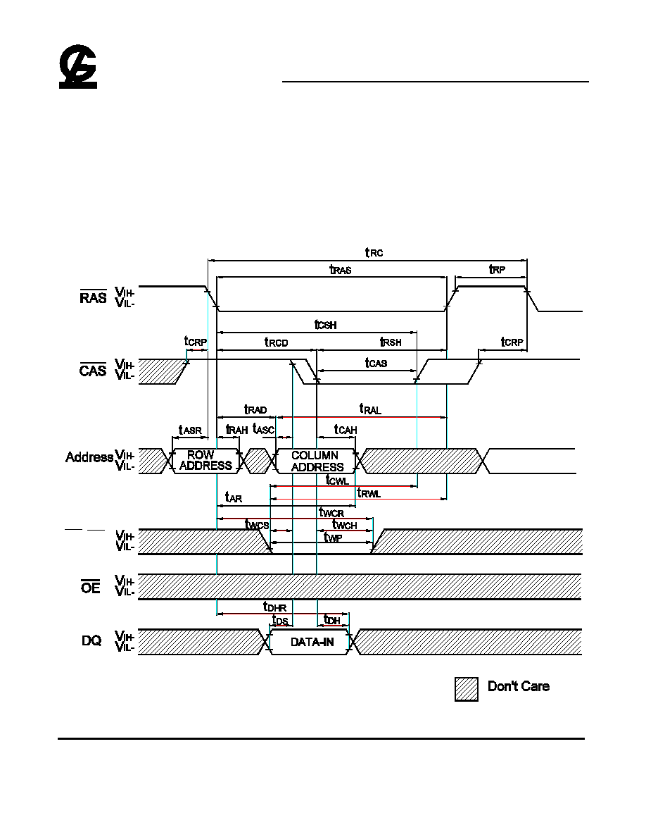
Read Cycle
Note : D
IN
= OPEN
UW,LW
G -LINK
GLT41316
64K X 16 CMOS DYNAMIC RAM WITH FAST PAGE MODE
June 1998 (Rev 2)
G-Link Technology Corporation
2701Northwestern Parkway
Santa Clara, CA 95051, U.S.A.
G-Link Technology Corporation, Taiwan
2F, No.12, R&D Rd. II, Science-Based Industrial Park,
Hsin Chu, Taiwan, R.O.C.
- 10 -
Early Write Cycle
NOTE : D
OUT
= OPEN
UW,LW

G -LINK
GLT41316
64K X 16 CMOS DYNAMIC RAM WITH FAST PAGE MODE
June 1998 (Rev 2)
G-Link Technology Corporation
2701Northwestern Parkway
Santa Clara, CA 95051, U.S.A.
G-Link Technology Corporation, Taiwan
2F, No.12, R&D Rd. II, Science-Based Industrial Park,
Hsin Chu, Taiwan, R.O.C.
- 11 -
Late Write Cycle ( OE Controlled Write)
NOET : D
OUT
= OPEN
UW,LW

G -LINK
GLT41316
64K X 16 CMOS DYNAMIC RAM WITH FAST PAGE MODE
June 1998 (Rev 2)
G-Link Technology Corporation
2701Northwestern Parkway
Santa Clara, CA 95051, U.S.A.
G-Link Technology Corporation, Taiwan
2F, No.12, R&D Rd. II, Science-Based Industrial Park,
Hsin Chu, Taiwan, R.O.C.
- 12 -
Read - Modify - Write Cycle
UW,LW

G -LINK
GLT41316
64K X 16 CMOS DYNAMIC RAM WITH FAST PAGE MODE
June 1998 (Rev 2)
G-Link Technology Corporation
2701Northwestern Parkway
Santa Clara, CA 95051, U.S.A.
G-Link Technology Corporation, Taiwan
2F, No.12, R&D Rd. II, Science-Based Industrial Park,
Hsin Chu, Taiwan, R.O.C.
- 13 -
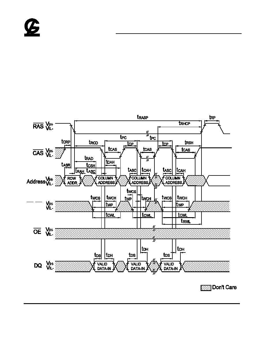
Fast Page Read Cycle
UW,LW
G -LINK
GLT41316
64K X 16 CMOS DYNAMIC RAM WITH FAST PAGE MODE
June 1998 (Rev 2)
G-Link Technology Corporation
2701Northwestern Parkway
Santa Clara, CA 95051, U.S.A.
G-Link Technology Corporation, Taiwan
2F, No.12, R&D Rd. II, Science-Based Industrial Park,
Hsin Chu, Taiwan, R.O.C.
- 14 -
Fast Page Early Write Cycle
NOTE : D
OUT
= OPEN
UW,LW

G -LINK
GLT41316
64K X 16 CMOS DYNAMIC RAM WITH FAST PAGE MODE
June 1998 (Rev 2)
G-Link Technology Corporation
2701Northwestern Parkway
Santa Clara, CA 95051, U.S.A.
G-Link Technology Corporation, Taiwan
2F, No.12, R&D Rd. II, Science-Based Industrial Park,
Hsin Chu, Taiwan, R.O.C.
- 15 -
Fast Page Mode Late Write Cycle
UW,LW

G -LINK
GLT41316
64K X 16 CMOS DYNAMIC RAM WITH FAST PAGE MODE
June 1998 (Rev 2)
G-Link Technology Corporation
2701Northwestern Parkway
Santa Clara, CA 95051, U.S.A.
G-Link Technology Corporation, Taiwan
2F, No.12, R&D Rd. II, Science-Based Industrial Park,
Hsin Chu, Taiwan, R.O.C.
- 16 -
Fast Page Read-Modify-Write Cycle
NOTE : D
OUT
= OPEN
UW,LW
G -LINK
GLT41316
64K X 16 CMOS DYNAMIC RAM WITH FAST PAGE MODE
June 1998 (Rev 2)
G-Link Technology Corporation
2701Northwestern Parkway
Santa Clara, CA 95051, U.S.A.
G-Link Technology Corporation, Taiwan
2F, No.12, R&D Rd. II, Science-Based Industrial Park,
Hsin Chu, Taiwan, R.O.C.
- 17 -
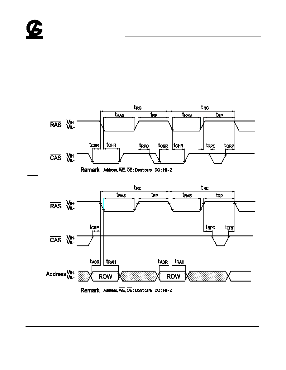
CAS Before RAS Refresh Cycle
RAS-Only Refresh Cycle
G -LINK
GLT41316
64K X 16 CMOS DYNAMIC RAM WITH FAST PAGE MODE
June 1998 (Rev 2)
G-Link Technology Corporation
2701Northwestern Parkway
Santa Clara, CA 95051, U.S.A.
G-Link Technology Corporation, Taiwan
2F, No.12, R&D Rd. II, Science-Based Industrial Park,
Hsin Chu, Taiwan, R.O.C.
- 18 -
Hidden Refresh Cycle ( Read )
UW,LW
G -LINK
GLT41316
64K X 16 CMOS DYNAMIC RAM WITH FAST PAGE MODE
June 1998 (Rev 2)
G-Link Technology Corporation
2701Northwestern Parkway
Santa Clara, CA 95051, U.S.A.
G-Link Technology Corporation, Taiwan
2F, No.12, R&D Rd. II, Science-Based Industrial Park,
Hsin Chu, Taiwan, R.O.C.
- 19 -
Hidden Refresh Cycle ( Write )
NOTE : D
OUT
= OPEN
UW,LW

G -LINK
GLT41316
64K X 16 CMOS DYNAMIC RAM WITH FAST PAGE MODE
June 1998 (Rev 2)
G-Link Technology Corporation
2701Northwestern Parkway
Santa Clara, CA 95051, U.S.A.
G-Link Technology Corporation, Taiwan
2F, No.12, R&D Rd. II, Science-Based Industrial Park,
Hsin Chu, Taiwan, R.O.C.
- 20 -
Ordering Information
Part Number
SPEED
POWER
FEATURE
PACKAGE
GLT41316-30J4
30ns
Normal
FPM
SOJ 400mil 40L
GLT41316-35J4
35ns
Normal
FPM
SOJ 400mil 40L
GLT41316-40J4
40ns
Normal
FPM
SOJ 400mil 40L
GLT41316-45J4
45ns
Normal
FPM
SOJ 400mil 40L
GLT41316-30TC
30ns
Normal
FPM
TSOP 400mil 44L
GLT41316-35TC
35ns
Normal
FPM
TSOP 400mil 44L
GLT41316-40TC
40ns
Normal
FPM
TSOP 400mil 44L
GLT41316-45TC
45ns
Normal
FPM
TSOP 400mil 44L
Parts Numbers (Top Mark) Definition :
GLT 4 13 16 - 40 J4
Note : C
�
CDROM , H
�
HDD.
Example :
1.GLT710008-15T 1Mbit(128Kx8)15ns 5V SRAM PDIP(300mil)Package type.
2.GLT44016-40J4 4Mbit(256Kx16)40ns 5V DRAM SOJ(400mil)Package type.
4 : DRAM
6 : Standard
SRAM
7 : Cache SRAM
8 : Synchronous
Burst SRAM
-SRAM
064 : 8K
256 : 256K
512 : 512K
100 : 1M
-DRAM
10 : 1M(C/EDO)*
11 : 1M(C/FPM)*
12 : 1M(H/EDO)*
13 : 1M(H/FPM)*
20 : 2M(EDO)
21 : 2M(FPM)
40 : 4M(EDO)
41 : 4M(FPM)
80 : 8M(EDO)
81 : 8M(FPM)
*See note
VOLTAGE
Blank : 5V
L : 3.3V
M : Mix Voltage
CONFIG.
04 : x04
08 : x08
16 : x16
32 : x32
SPEED
-SRAM
12 : 12ns
15 : 15ns
20 : 20ns
70 : 70ns
-DRAM
30 : 30ns
35 : 35ns
40 : 40ns
45 : 45ns
50 : 50ns
60 : 60ns
PACKAGE
T : PDIP(300mil)
TS : TSOP(Type I)
TC : TSOP(Type ll)
PL : PLCC
FA : 300mil SOP
FB : 330mil SOP
FC : 445mil SOP
J3 : 300mil SOJ
J4 : 400mil SOJ
P : PDIP(600mil)
Q : PQFP
TQ : TQFP

G -LINK
GLT41316
64K X 16 CMOS DYNAMIC RAM WITH FAST PAGE MODE
June 1998 (Rev 2)
G-Link Technology Corporation
2701Northwestern Parkway
Santa Clara, CA 95051, U.S.A.
G-Link Technology Corporation, Taiwan
2F, No.12, R&D Rd. II, Science-Based Industrial Park,
Hsin Chu, Taiwan, R.O.C.
- 21 -
Package Information
400mil 40 pin Small Outline J-form Package (SOJ)
G -LINK
GLT41316
64K X 16 CMOS DYNAMIC RAM WITH FAST PAGE MODE
June 1998 (Rev 2)
G-Link Technology Corporation
2701Northwestern Parkway
Santa Clara, CA 95051, U.S.A.
G-Link Technology Corporation, Taiwan
2F, No.12, R&D Rd. II, Science-Based Industrial Park,
Hsin Chu, Taiwan, R.O.C.
- 22 -
40/44 Lead Thin Small Outline Package TSOP(Type II)