Äîêóìåíòàöèÿ è îïèñàíèÿ www.docs.chipfind.ru

G -LINK
GLT5640AL16
4M X 16 CMOS Synchronous Dynamic RAM
Feb 2004 (Rev.0.1)
G-Link Technology Corporation, Taiwan
Web : www.glink.com.tw Email : sales@glink.com.tw
TEL : 886-2-27968078
- 1 -
Description
The GLT5640AL16 are high-speed 67,108,864-bit synchronous dynamic random-access memories, organized as
1,048,576 x 16 x 4 (word x bit x bank), respectively.
The synchronous DRAMs achieved high-speed data transfer using the pipeline architecture and clock frequency up
to 183MHz. All input and outputs are synchronized with the positive edge of the clock. The synchronous DRAMs are
compatible with Low Voltage TTL (LVTTL).These products are packaged in 54-pin TSOPII.
Features
·
Single 3.3V ((
±
0.3V) power supply
· High speed clock cycle time -5.5:183MHz<3-3-3>,-6:166MHz<3-3-3>, -7:143MHz<3-3-3>, -8: 125MHz<3-3-3>
-10 : 100MHz<3-3-3>
· Fully synchronous operation referenced to clock rising edge
· Possible to assert random column access in every cycle
· Quad internal banks controlled by BA0 & BA1 (Bank Select)
· Byte control by LDQM and UDQM
· Programmable Wrap sequence (Sequential / Interleave)
· Programmable burst length (1, 2, 4, 8 and full page)
· Programmable /CAS latency (2 and 3)
· Automatic precharge and controlled precharge
· CBR (Auto) refresh and self refresh
· X16 organization
· LVTTL compatible inputs and outputs
· 4,096 refresh cycles / 64ms
· Burst termination by Burst stop and Precharge command
G -LINK
GLT5640AL16
4M X 16 CMOS Synchronous Dynamic RAM
Feb 2004 (Rev.0.1)
G-Link Technology Corporation, Taiwan
Web : www.glink.com.tw Email : sales@glink.com.tw
TEL : 886-2-27968078
- 2 -
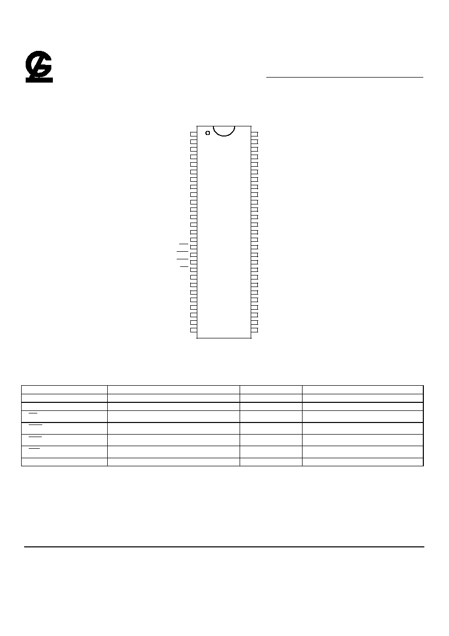
Pin Configurations
GLT5640AL16
1
2
3
4
5
6
7
9
10
11
12
13
8
14
15
16
39
40
41
42
43
44
45
46
47
48
49
50
51
52
53
54
V
DD
DQ
0
V
DDQ
DQ
1
DQ
2
V
SSQ
V
SS
DQ
15
17
18
19
20
21
22
23
24
A
10
A
0
25
26
27
A
3
A
2
28
29
30
31
32
33
34
35
36
37
38
A
11
DQ
3
DQ
4
V
DDQ
DQ
5
DQ
6
V
SSQ
DQ
7
V
DD
LDQM
WE
CAS
RAS
CS
BA0
BA1
A
1
V
DD
V
SSQ
DQ
14
DQ
13
V
DDQ
DQ
12
DQ
11
V
SSQ
DQ
10
DQ
9
V
DDQ
DQ
8
V
SS
NC
UDQM
CLK
CKE
NC
A
9
A
8
A
7
A
6
A
5
A
4
V
SS
Pin Descriptions
Pin Name
Function
Pin Name
Function
CLK
Master Clock
DQM
DQ Mask Enable
CKE
Clock Enable
A0-11
Address Input
CS
Chip Select
BA0,1
Bank Address
RAS
Row Address Strobe
VDD
Power Supply
CAS
Column Address Strobe
VDDQ
Power Supply for DQ
WE
Write Enable
VSS
Ground
DQ0 ~ DQ15
Data I/O
VSSQ
Ground for DQ
G -LINK
GLT5640AL16
4M X 16 CMOS Synchronous Dynamic RAM
Feb 2004 (Rev.0.1)
G-Link Technology Corporation, Taiwan
Web : www.glink.com.tw Email : sales@glink.com.tw
TEL : 886-2-27968078
- 3 -
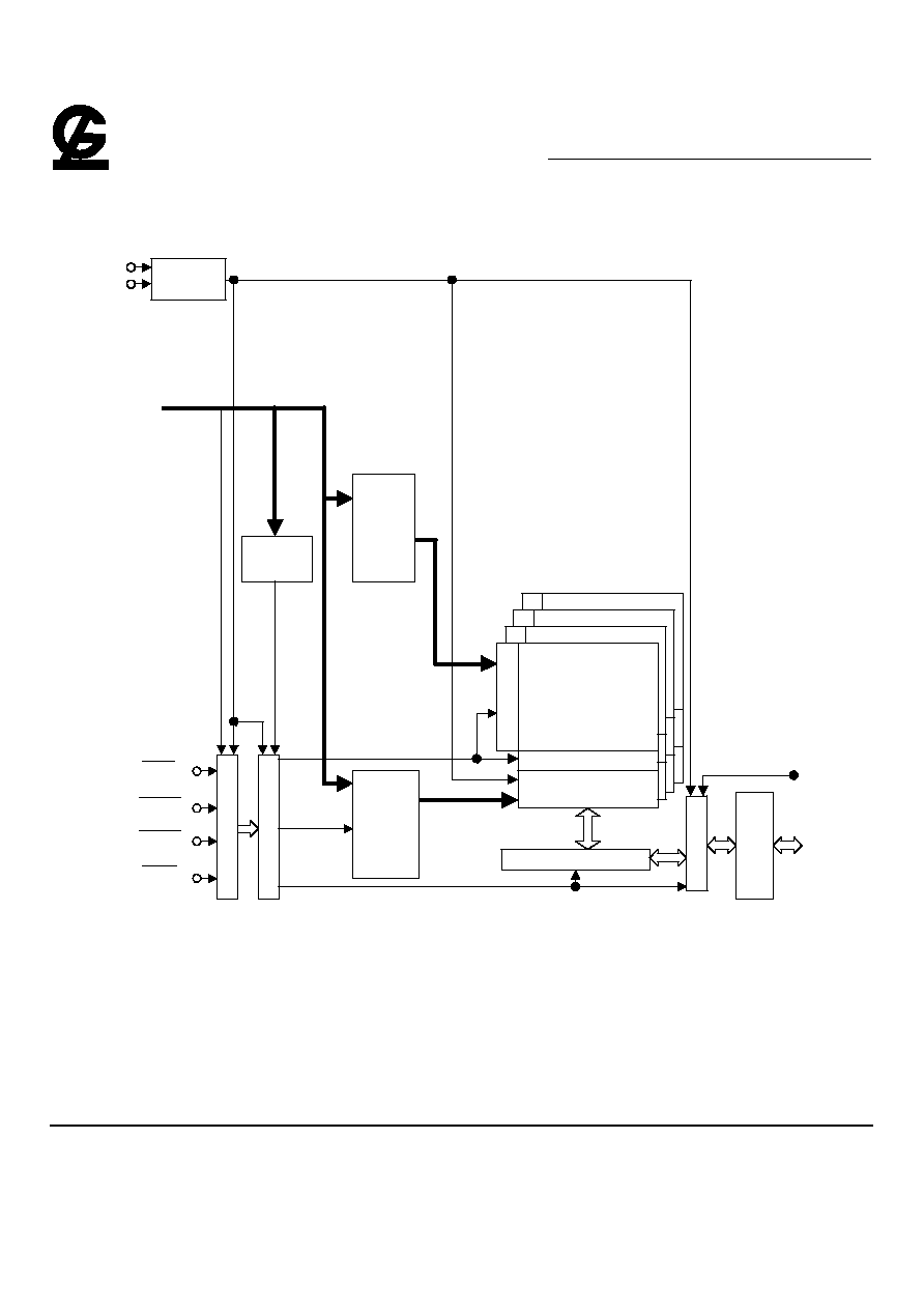
Block Diagram
CLK
CKE
Clock
Generator
Command Decoder
Control Logic
Mode
Register
Column
Address
Buffer
&
Burst
counter
Row
Address
Buffer
&
Burst
counter
Row Decoder
Column Decoder &
Latch Circuoit
Sense amplifier
Bank B
Bank C
Bank D
Bank A
Data Control Circuit
Latch Circuit
Input & Output
Buffer
DQ
DQM
Address
CS
RAS
CAS
WE
G -LINK
GLT5640AL16
4M X 16 CMOS Synchronous Dynamic RAM
Feb 2004 (Rev.0.1)
G-Link Technology Corporation, Taiwan
Web : www.glink.com.tw Email : sales@glink.com.tw
TEL : 886-2-27968078
- 4 -
Pin Function
Symbol
Input
Function
CLK
Input
Master Clock: Other inputs signals are referenced to the CLK rising edge
CKE
Input
Clock Enable: CKE HIGH activates, and CKE LOW deactivates internal clock signals, device
input buffers and output drivers. Deactivating the clock provides PRECHARGE POWER-DOWN
and SELF REFRESH operation (all banks idle), or ACTIVE POWER-DOWN (row ACTIVE in any
bank).
CS
Input
Chip Select:
CS
enables (registered LOW) and disables (registered HIGH) the command
decoder. All commands are masked when
CS
is registered HIGH.
CS
provides for external
bank selection on systems with multiple banks.
CS
is considered part of the command code.
RAS
,
CAS
,
WE
Input
Command Inputs:
RAS
,
CAS
and
WE
(along with
CS
) define the command being entered.
A0 - A13
Input
Address Inputs: Provide the row address for ACTIVE commands, and the column address and
AUTO PRECHARGE bit for READ/WRITE commands, to select one location out of the memory
array in the respective bank. The row address is specified by A0-A11. The column address is
specified by A0-A7
BA0,BA1
Input
Bank Address Inputs: BA0 and BA1 define to which bank an ACTIVE, READ, WRITE or
PRECHARGE command is being applied.
DQM, UDQM ,
LDQM
Input
Din Mask / Output Disable : When DQM is high in burst write, Din for the current cycle is
masked. When DQM is high in burst read, Dout is disable (two - clock latency).
DQ0 - DQ15
I/O
Data Input / Output: Data bus
VDD, VSS
Supply
Power Supply for the memory array and peripheral circuitry
VDDQ, VSSQ
Supply
Power Supply are supplied to the output buffers only
G -LINK
GLT5640AL16
4M X 16 CMOS Synchronous Dynamic RAM
Feb 2004 (Rev.0.1)
G-Link Technology Corporation, Taiwan
Web : www.glink.com.tw Email : sales@glink.com.tw
TEL : 886-2-27968078
- 5 -
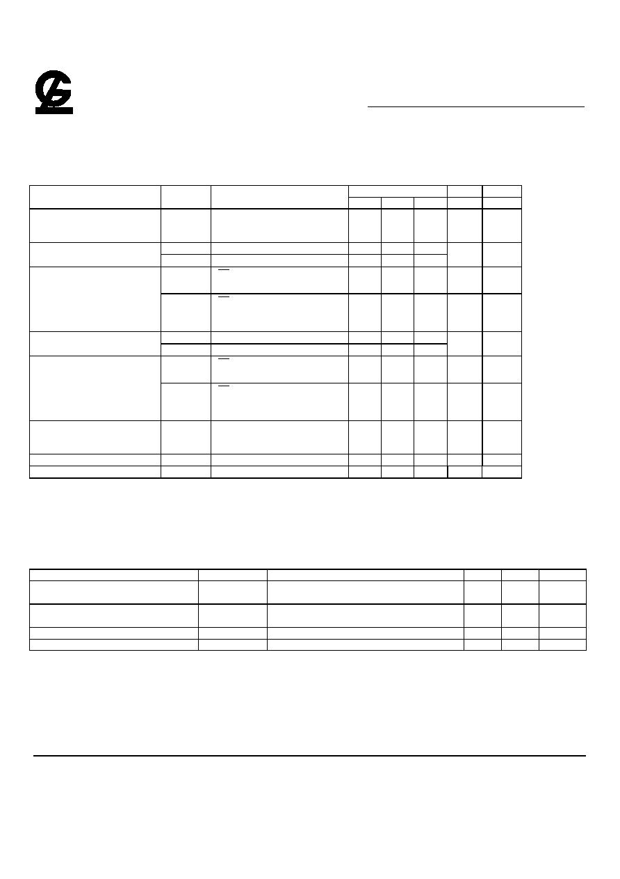
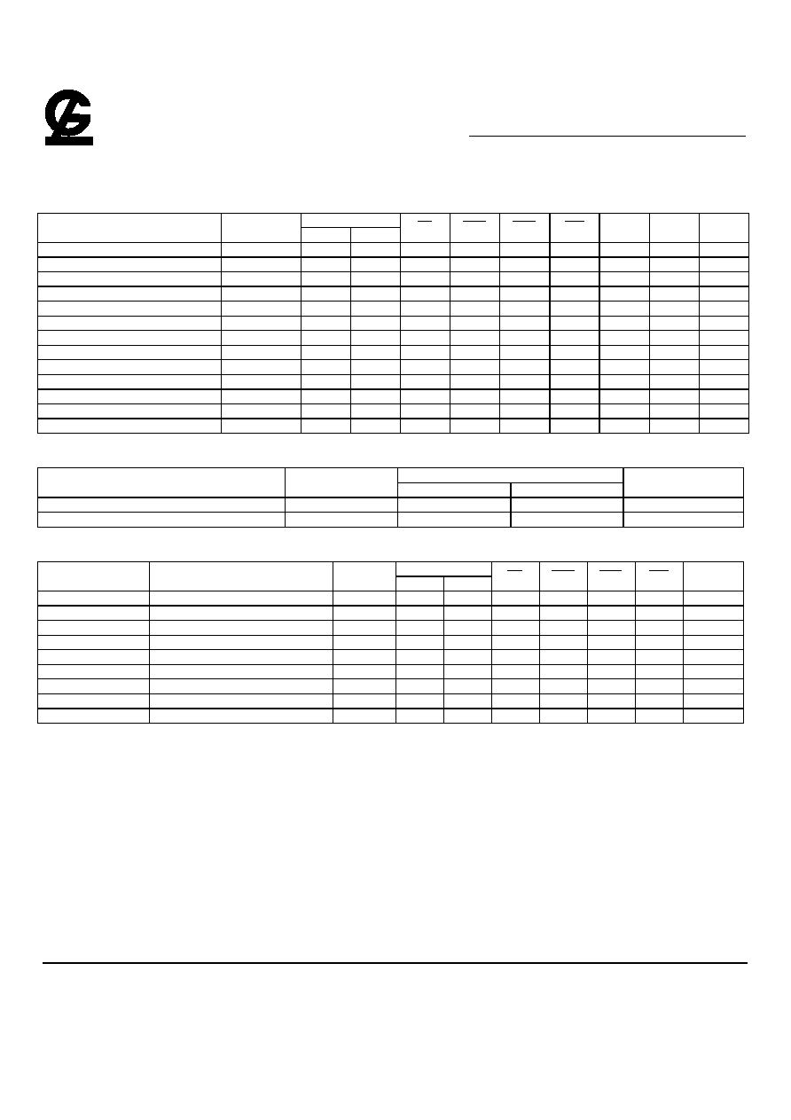
Absolute Maximum Ratings
Parameter
Symbol
Conditions
Value
Unit
Supply Voltage
VDD
with respect to VSS
-0.5 to 4.6
V
Supply Voltage for Output
VDDQ
with respect to VSSQ
-0.5 to 4.6
V
Input Voltage
VI
with respect to VSS
-0.5 to VDD+0.5
V
Output Voltage
VO
with respect to VSSQ
-0.5 to VDDQ+0.5
V
Short circuit output current
IO
50
mA
Power dissipation
PD
Ta = 25 °C
1
W
Operating temperature
TOPT
0 to 70
°C
Storage temperature
TSTG
-65 to 150
°C
Caution Exposing the device to stress above those listed in Absolute Maximum Ratings could cause permanent damage. The device is not meant to be
operated under conditions outside the limits described in the operational section of this specification. Exposure to Absolute Maximum Rating conditions for
extended periods may affect device reliability.
Recommended Operating Conditions (Ta = 0 ~ 70 °C, unless otherwise noted)
Parameter
Symbol
Limits
Unit
Min.
Typ.
Max.
Supply Voltage
VDD
3.0
3.3
3.6
V
Supply Voltage for DQ
VDDQ
3.0
3.3
3.6
V
Ground
VSS
0
0
0
V
Ground for DQ
VSSQ
0
0
0
V
High Level Input Voltage (all inputs)
VIH
2.0
VDD + 0.3
V
Low Level Input Voltage (all inputs)
VIL
-0.3
0.8
V
Note :
1.All voltages are referenced to Vss = 0V.
2.VIH (max) is acceptable 5.6V AC pulse width with
3ns of duration.
3.VIL (min) is acceptable -2.0V AC pulse width with
3ns of duration.
Pin Capacitance (Ta = 0 ~ 70°C, V
DD
= V
DDQ
= 3.3
±
±
0.3V , V
SS
= V
SSQ
= 0V, unless otherwise noted)
Parameter
Symbol
Min
Max
Unit
Input Capacitance, address & control pin
CIN
2.5
3.8
pF
Input Capacitance, CLK pin
CCLK
2.5
3.5
pF
Data input / output capacitance
CI/O
4.0
6.5
pF
G -LINK
GLT5640AL16
4M X 16 CMOS Synchronous Dynamic RAM
Feb 2004 (Rev.0.1)
G-Link Technology Corporation, Taiwan
Web : www.glink.com.tw Email : sales@glink.com.tw
TEL : 886-2-27968078
- 6 -
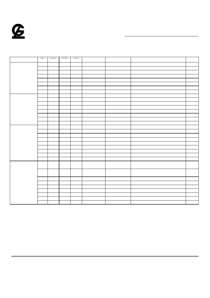
DC Characteristics 1
(Ta = 0 ~ 70°C, V
DD
= V
DDQ
= 3.3
±
±
0.3V, V
SS
= V
SSQ
= 0V, Output Open, unless otherwise noted)
Limits(max.)
Unit
Notes
Parameter
Symbol
Test Conditions
-5.5
-6
-7
Operating current
I
CC1
One bank active
t
RC
= t
RC(MIN)
, t
CLK
= t
CLK(MIN)
,
BL = 1, CL=3
105
100
95
mA
1
I
CC2
P
CKE
V
IL(MAX),
t
CK
= 15ns
2
2
2
Precharge standby current
in power down mode
I
CC2
PS
CKE
V
IL(MAX)
, CLK
V
IL(MAX)
1
1
1
mA
I
CC2
N
CS
V
DD
- 0.2V
t
CK
= 15ns, CKE
V
IH(MIN)
20
20
20
mA
2
Precharge standby current
in non power down mode
I
CC2
NS
CS
V
DD
- 0.2V
CLK
V
IL(MAX),
CKE
V
IH(MIN)
All input signals are stable.
20
20
20
mA
I
CC3
P
CKE
V
IL(MAX)
, t
CK
= 10ns
7
7
7
Active standby current in
power down mode
I
CC3
PS
CKE
V
IL(MAX)
, CLK
V
IL(MAX)
5
5
5
mA
I
CC3
N
CS
V
DD
- 0.2V
t
CK
= 15ns, CKE
V
IH(MIN)
35
35
35
mA
2
Active standby current in
Nonpower down mode
I
CC3
NS
CS
V
DD
- 0.2V
CLK
V
IL(MAX),
CKE
V
IH(MIN)
All input signals are stable.
35
35
35
mA
Operating current
(Burst mode)
I
CC4
All banks active
t
CK
= t
CK(MIN)
, BL=4, CL=3
All banks active
140
130
120
mA
Refresh current
I
CC5
t
RC
= t
RC(MIN)
, t
CLK
= t
CLK(MIN)
180
170
160
mA
Self refresh current
I
CC6
CKE
0.2V
1
1
1
mA
NOTES
1. I
CC(max)
is specified at the output open condition.
2. Input signals are changed one time during 30ns.
DC Characteristics 2
(Ta = 0 ~ 70°C, V
DD
= V
DDQ
= 3.3
±
±
0.3V , V
SS
= V
SSQ
= 0V, unless otherwise noted)
Parameter
Symbol
Test Condition
Min
Max
Unit
Input leakage current (Inputs)
I
I
(L)
0
V
IN
V
DD
(MAX)
Pins not under test = 0V
5
5
uA
Output leakage current (I/O pins)
I
O
(L)
0
V
OUT
V
DD
(MAX)
DQ# in H - Z., D
OUT
is disabled
5
5
uA
High level output voltage
V
OH
I
OH
= -2mA
2.4
V
Low level output voltage
V
OL
I
OL
= 2mA
0.4
V
G -LINK
GLT5640AL16
4M X 16 CMOS Synchronous Dynamic RAM
Feb 2004 (Rev.0.1)
G-Link Technology Corporation, Taiwan
Web : www.glink.com.tw Email : sales@glink.com.tw
TEL : 886-2-27968078
- 7 -
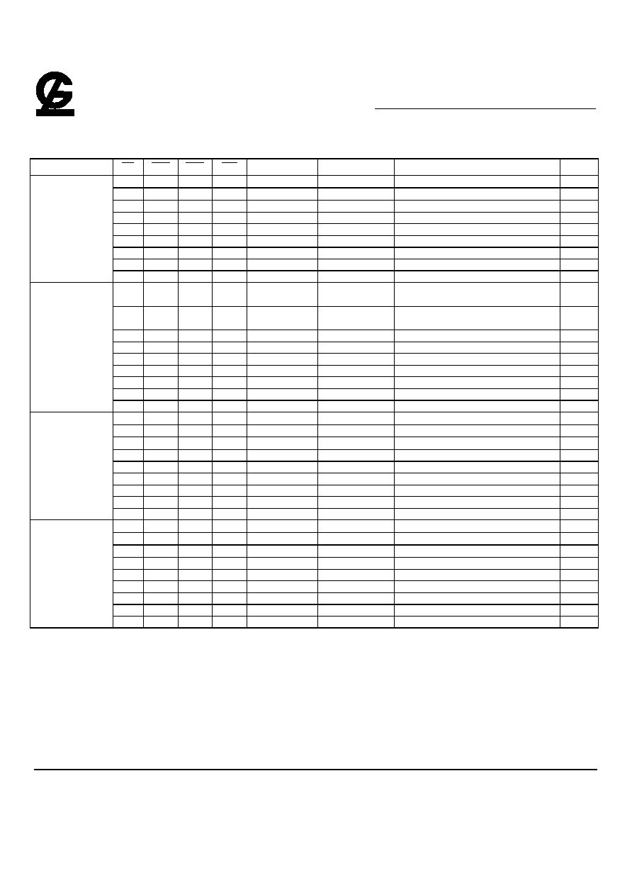
AC Characteristics (Ta = 0 ~ 70°C, V
DD
= V
DDQ
= 3.3
±
±
0.3V , V
SS
= V
SSQ
= 0V, unless otherwise noted)
Test Conditions
AC input Levels (VIH/VIL)
2.0 / 0.8V
Input timing reference level /
Output timing reference level
1.4V
Input rise and fall time
1ns
Output load condition
50pF
Note): 1.if clock rising time is longer than 1ns, (tr/2-0.5ns) should be added to the parameter.
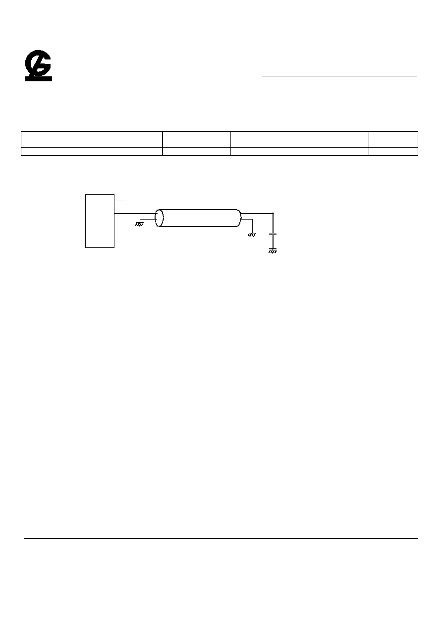
Output Load Conditions
V
DDQ
V
DDQ
V
OUT
Device
Under
Test
50PF
Z = 50
G -LINK
GLT5640AL16
4M X 16 CMOS Synchronous Dynamic RAM
Feb 2004 (Rev.0.1)
G-Link Technology Corporation, Taiwan
Web : www.glink.com.tw Email : sales@glink.com.tw
TEL : 886-2-27968078
- 8 -
Switching Characteristics (Ta = 0 ~ 70°C, V
DD
= V
DDQ
= 3.3
±
±
0.3V , V
SS
= V
SSQ
= 0V, unless otherwise noted)
Limits
5.5
-6
-7
Parameter
Symbol
Min
Max
Min
Max
Min
Max
Unit
Note
CLK cycle time
CL=3
t
CK3
5.5
6
7
ns
CL=2
t
CK2
-
8
9
ns
CLK high pulse width
t
CH
2.3
2.5
2.5
ns
CLK low pulse width
t
CL
2.3
2.5
2.5
ns
Transition time of CLK
t
T
1
10
1
10
1
10
ns
Input Setup time
t
IS
1.5
1.5
1.5
ns
1
Input Hold time
t
IH
1
1
1
ns
2
Row Cycle Time
t
RC
55
60
63
ns
Refresh Cycle Time
t
RFC
55
60
70
ns
Row to Column Delay
t
RCD
16.5
18
21
ns
Row active time
t
RAS
38.5
100k
42
100k
45
100k
ns
Row Precharge time
t
RP
16.5
18
21
ns
Write Recovery time
t
WR
11
12
14
ns
3
Act to Delay time
t
RRD
11
12
14
ns
Mode Register Set Cycle time
t
RSC
2
2
2
t
CK
Data-in to ACTIVE command
t
DAL
5
5
5
t
CK
Refresh Interval time
t
REF
64
64
64
ms
Note :
1. t
IS
= t
CKS
(CKE setup time) , t
CMS
(Command setup time) , t
AS
(Address setup time) , t
DS
(Input data setup time).
2. t
IH
= t
CKH
(CKE hold time) , t
CMH
(Command hold time) , t
AH
(Address hold time) , t
DH
(Input data hold time).
3. t
WR
is so called t
DPL
.
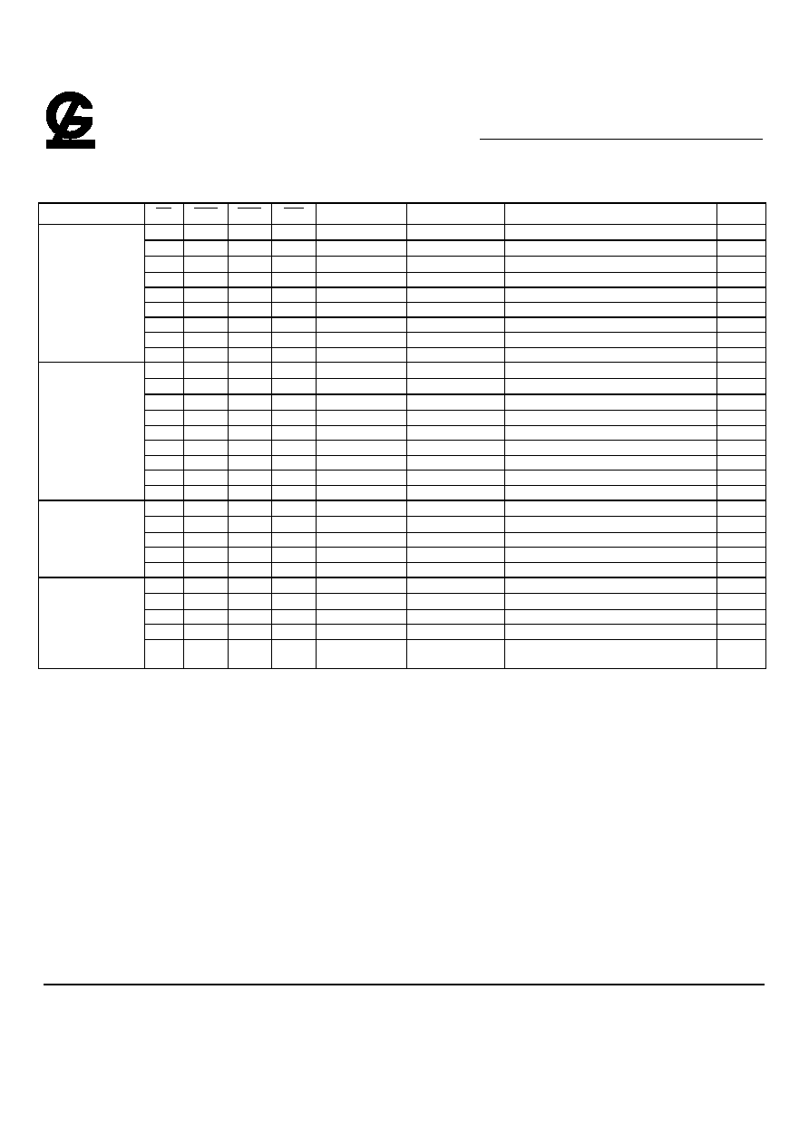
Switching Characteristics (Ta = 0 ~ 70°C, V
DD
= V
DDQ
= 3.3
±
±
0.3V , V
SS
= V
SSQ
= 0V, unless otherwise noted)
Limits
-5.5
-6
-7
Unit
Note
Parameter
Symbol
Min
Max
Min
Max
Min
Max
CL = 3
t
AC3
5
5
5.5
ns
*1
Access time from CLK
CL = 2
t
AC2
6
6
6
ns
*1
CL = 3
t
CH3
2
2.5
2.5
ns
*1
Output Hold time from CLK
CL = 2
t
CH2
2
2.5
2.5
ns
*1
Delay time , output low-impedance
from CLK
t
OLZ
0
0
0
ns
Delay time , output high-impedance
from LCK
t
OHZ
2
5
2.5
5
2.5
5.5
ns
Note :
1. If clock rising time is longer than 1ns, (tr/2-0.5ns) should be added to the parameter.
G -LINK
GLT5640AL16
4M X 16 CMOS Synchronous Dynamic RAM
Feb 2004 (Rev.0.1)
G-Link Technology Corporation, Taiwan
Web : www.glink.com.tw Email : sales@glink.com.tw
TEL : 886-2-27968078
- 9 -
Basic Features and Function Description
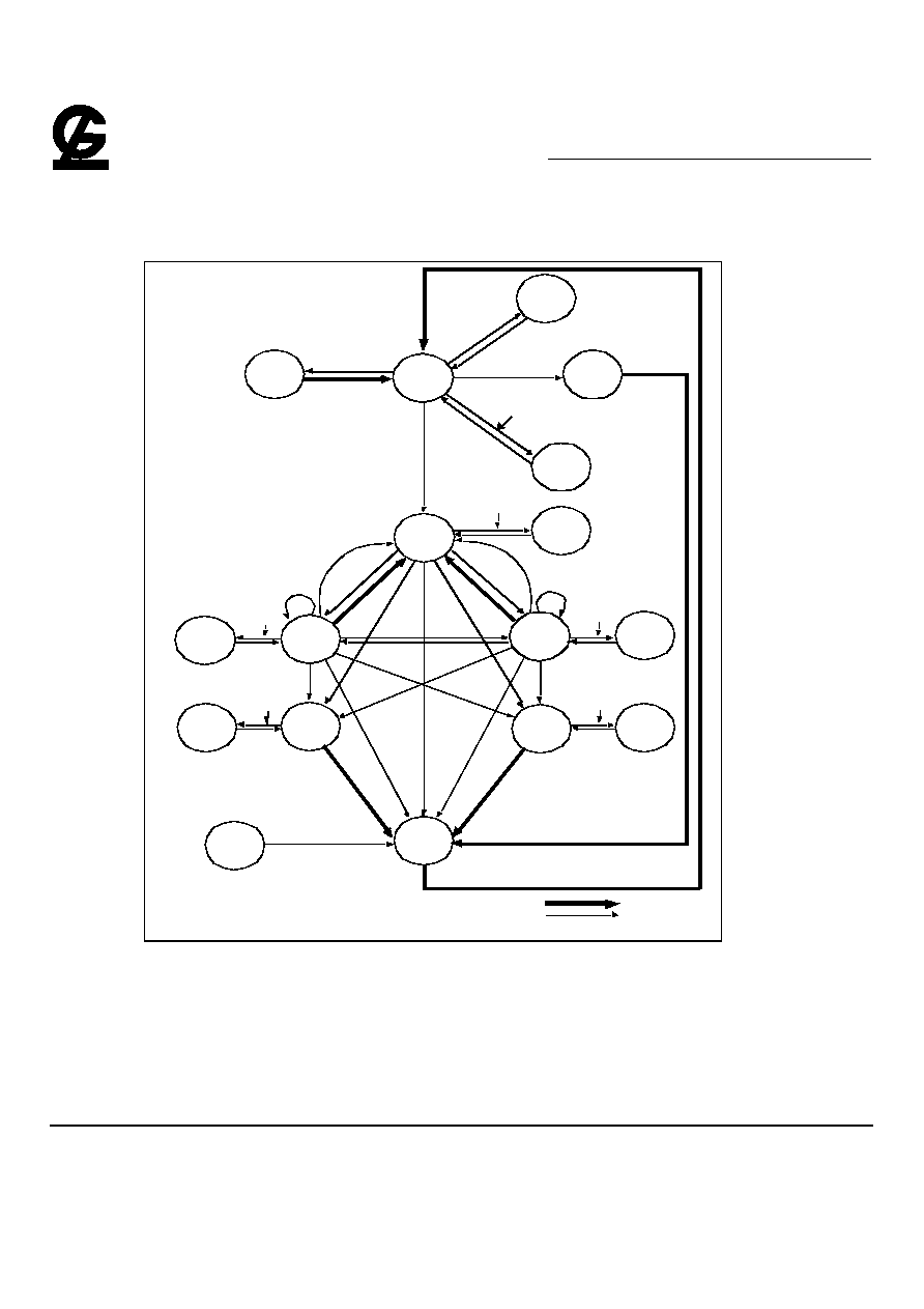
1. Simplified State Diagram
Self
Refresh
MRS
Mode
Register
Set
IDLE
AUTO
Refresh
REF
A
C
T
CKE
CKE
BS
T
Power
Down
Active
Power
Down
R O W
ACTIVE
Read
CKE
CKE
READ
READ
SUSPEND
CKE
CKE
READ A
READA
SUSPEND
Read with
Auto Precharge
CKE
CKE
Write (Write recovery)
WRITE
WRITE
SUSPEND
WRITE A
WRITE A
SUSPEND
CKE
CKE
Write with
Aut o Precharge
POWER
ON
Precharge
Precharge
P
R
E
(P
r e
ch
a
r g
e
te
rm
in
a
tio
n
)
P
R
E
(
P
r e
ch
ar
g
e
te
rm
in
a
tio
n)
R
e
a
d
w
ith
W
rit
e
w
ith
A
u
to
p
re
dh
a
rg
e
A
u
to
P
re
ch
a
rg
e
R
ea
d
B
ST
W
ri t
e
Rea
d with
A
uto P r
echar
ge
(write
reco
very )
Wr
ite
with
Au
t o
Pre
ch
arg
e
Write
Read (write recovery)
P
R
E
CK
E
C
K E
Automatic sequence
Manual input
Note: After the AUTO refresh operation, precharge operation is
performed automatically and enter the IDLE state
SE
L F
en
try
SE
L F
e
xit
W
rit
e
r
ec
o
ve
ry
G -LINK
GLT5640AL16
4M X 16 CMOS Synchronous Dynamic RAM
Feb 2004 (Rev.0.1)
G-Link Technology Corporation, Taiwan
Web : www.glink.com.tw Email : sales@glink.com.tw
TEL : 886-2-27968078
- 10 -
2.Truth Table
2.1 Command Truth Table
CKE
FUNCTION
Symbol
n - 1
n
CS
RAS
CAS
WE
BA
A10
A11
A9 A0
Device deselect
DESL
H
X
H
X
X
X
X
X
X
No operation
NOP
H
X
L
H
H
H
X
X
X
Mode register set
MRS
H
X
L
L
L
L
L
L
V
Bank activate
ACT
H
X
L
L
H
H
V
V
V
Read
READ
H
X
L
H
L
H
V
L
V
Read with auto precharge
READA
H
X
L
H
L
H
V
H
V
Write
WRIT
H
X
L
H
L
L
V
L
V
Write with auto precharge
WRITA
H
X
L
H
L
L
V
H
V
Precharge select bank
PRE
H
X
L
L
H
L
V
L
X
Precharge all banks
PALL
H
X
L
L
H
L
X
H
X
Burst stop
BST
H
X
L
H
H
L
X
X
X
CBR (Auto) refresh
REF
H
H
L
L
L
H
X
X
X
Self refresh
SELF
H
L
L
L
L
H
X
X
X
2.2 DQM Truth Table
CKE
FUNCTION
Symbol
n - 1
n
DQM
Data write/output enable
ENB
H
X
L
Data mask/output disable
MASK
H
X
H
2.3 CKE Truth Table
CKE
Current State
Function
Symbol
n - 1
n
CS
RAS
CAS
WE
Address
Activating
Clock suspend mode entry
H
L
X
X
X
X
X
Any
Clock suspend
L
L
X
X
X
X
X
Clock suspend
Clock suspend mode exit
L
H
X
X
X
X
X
Idle
CBR refresh command
REF
H
H
L
L
L
H
X
Idle
Self refresh entry
SELF
H
L
L
L
L
H
X
Self refresh
Self refresh exit
L
H
L
H
H
H
X
L
H
H
X
X
X
X
Idle
Power down entry
H
L
X
X
X
X
X
Power down
Power down exit
L
H
X
X
X
X
X
H : High level, L : Low level
X : High or Low level (Don't care), V : Valid Data input
G -LINK
GLT5640AL16
4M X 16 CMOS Synchronous Dynamic RAM
Feb 2004 (Rev.0.1)
G-Link Technology Corporation, Taiwan
Web : www.glink.com.tw Email : sales@glink.com.tw
TEL : 886-2-27968078
- 11 -
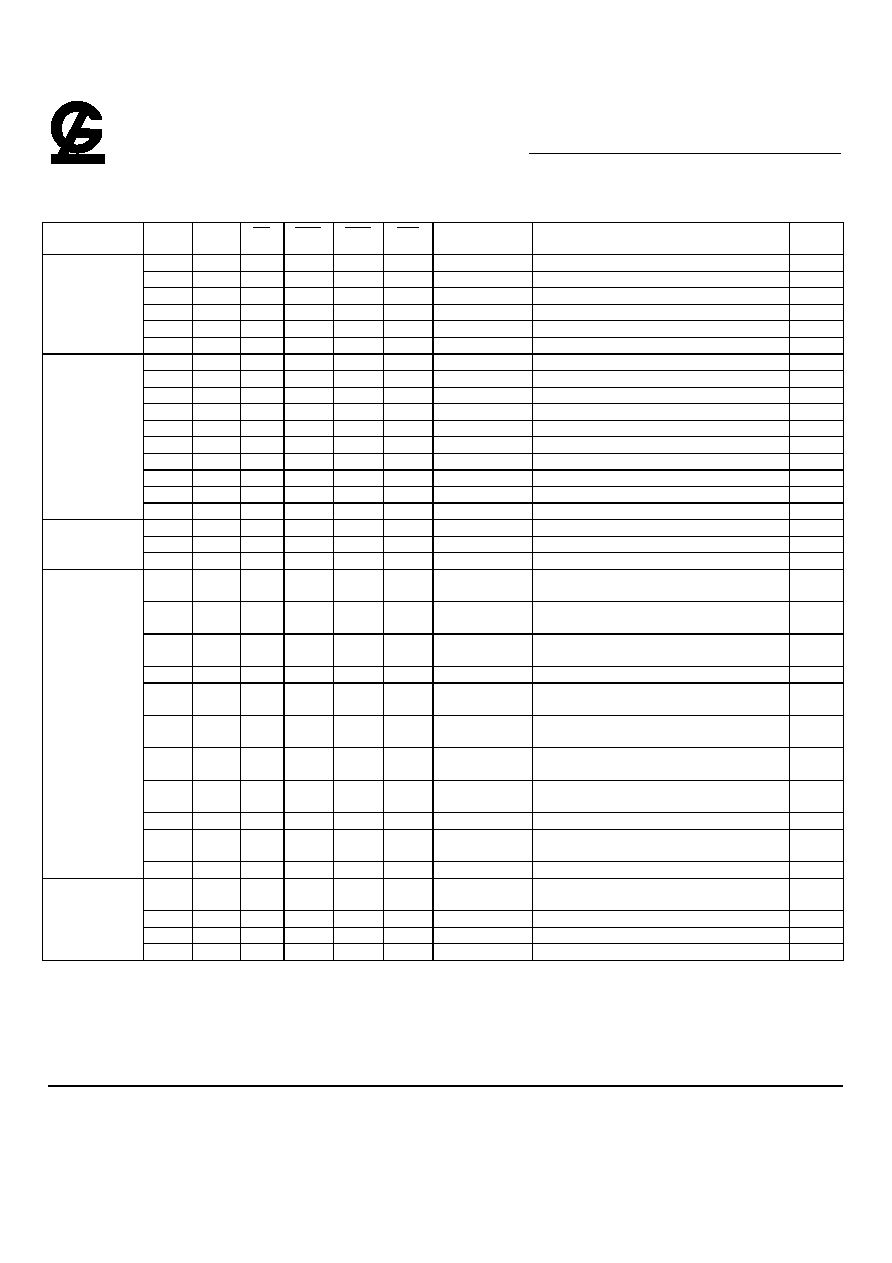
2.4 Operative Command Table (note 1)
Current state
CS
RAS
CAS
WE
Address
Command
Action
Notes
H
X
X
X
X
DESL
Nop or Power down
2
L
H
H
X
X
NOP or BST
Nop or Power down
2
L
H
L
H
BA, CA, A10
READ/READA
ILLEGAL
3
L
H
L
L
BA, CA, A10
WRIT/WRITA
ILLEGAL
3
L
L
H
H
BR, RA
ACT
Row active
L
L
H
L
BA, A10
PRE/PALL
Nop
L
L
L
H
X
REF/SELF
Refresh or Self refresh
4
Idle
L
L
L
L
Op-Code
MPS
Mode register access
H
X
X
X
X
DESL
Nop
L
H
H
X
X
NOP or BST
Nop
L
H
L
H
BA, CA, A10
READ/READA
Begin read : Determine AP
5
L
H
L
L
BA, CA, A10
WRIT/WRITA
Begin write : Determine AP
5
L
L
H
H
BA, RA
ACT
ILLEGAL
3
L
L
H
L
BA, A10
PRE/PALL
Precharge
6
L
L
L
H
X
REF/SELF
ILLEGAL
Row active
L
L
L
L
Op-Code
MRS
ILLEGAL
H
X
X
X
X
DESL
Continue burst to end
Row active
L
H
H
H
X
NOP
Continue burst to end
Row active
L
H
H
L
X
BST
Burst stop
Row active
L
H
L
H
BA, CA, A10
READ/READA
Term burst, new read : Determine AP
7
L
H
L
L
BA, CA, A10
WRIT/WRITA
Term burst, start write : Determine AP
7,8
L
L
H
H
BA, RA
ACT
ILLEGAL
3
L
L
H
L
BA, A10
PRE/PALL
Term burst, precharging
L
L
L
H
X
REF/SELF
ILLEGAL
Read
L
L
L
L
Op-Code
MRS
ILLEGAL
H
X
X
X
X
DESL
Continue burst to end
write
recovering
L
H
H
H
X
NOP
Continue burst to end
write
recovering
L
H
H
L
X
BST
Burst stop
Row active
L
H
L
H
BA, CA, A10
READ/READA
Term burst, start read : Determine AP
7,8
L
H
L
L
BA, CA, A10
WRIT/WRITA
Term burst, new write : Determine AP
7
L
L
H
H
BA, RA
ACT
ILLEGAL
3
L
L
H
L
BA, A10
PRE/PALL
Term burst, precharging
9
L
L
L
H
X
REF/SELF
ILLEGAL
write
L
L
L
L
Op-Code
MRS
ILLEGAL
G -LINK
GLT5640AL16
4M X 16 CMOS Synchronous Dynamic RAM
Feb 2004 (Rev.0.1)
G-Link Technology Corporation, Taiwan
Web : www.glink.com.tw Email : sales@glink.com.tw
TEL : 886-2-27968078
- 12 -
Current state
CS
RAS
CAS
WE
Address
Command
Action
Notes
H
X
X
X
X
DESL
Continue burst to end
Precharging
L
H
H
H
X
NOP
Continue burst to end
Precharging
L
H
H
L
X
BST
ILLEGAL
L
H
L
H
BA, CA, A10
READ/READA
ILLEGAL
11
L
H
L
L
BA, CA, A10
WRIT/WRITA
ILLEGAL
11
L
L
H
H
BA, RA
ACT
ILLEGAL
3,11
L
L
H
L
BA, A10
PRE/PALL
ILLEGAL
3,11
L
L
L
H
X
PEF/SELF
ILLEGAL
Read with auto
precharge
L
L
L
L
Op - Code
MRS
ILLEGAL
H
X
X
X
X
DESL
Continue burst to end
write
recovering with auto precharge
L
H
H
H
X
NOP
Continue burst to end
write
recovering with auto precharge
L
H
H
L
X
BST
ILLEGAL
L
H
L
H
BA, CA, A10
READ/READA
ILLEGAL
11
L
H
L
L
BA, CA, A10
WRIT/WRITA
ILLEGAL
11
L
L
H
H
BA, RA
ACT
ILLEGAL
3,11
L
L
H
L
BA, A10
PRE/PALL
ILLEGAL
3,11
L
L
L
H
X
REF/SELF
ILLEGAL
Write with auto
precharge
L
L
L
L
Op - code
MRS
ILLEGAL
H
X
X
X
X
DESL
Nop
Enter idle after tRP
L
H
H
H
X
NOP
Nop
Enter idle after tRP
L
H
H
L
X
BST
Nop
Enter idle after tRP
L
H
L
H
BA, CA, A10
READ/READA
ILLEGAL
3
L
H
L
L
BA, CA, A10
WRIT/WRITA
ILLEGAL
3
L
L
H
H
BA, RA
ACT
ILLEGAL
3
L
L
H
L
BA, A10
PRE/PALL
Nop Enter idle after tRP
L
L
L
H
X
REF/SELF
ILLEGAL
Precharging
L
L
L
L
Op - Code
MRS
ILLEGAL
H
X
X
X
X
DESL
Nop
Enter row active after tRCD
L
H
H
H
X
NOP
Nop
Enter row active after tRCD
L
H
H
L
X
BST
Nop
Enter row active after tRCD
L
H
L
H
BA, CA, A10
READ/READA
ILLEGAL
3
L
H
L
L
BA, CA, A10
WRIT/WRITA
ILLEGAL
3
L
L
H
H
BA, RA
ACT
ILLEGAL
3, 9
L
L
H
L
BA, A10
PRE/PALL
ILLEGAL
3
L
L
L
H
X
REF/SELF
ILLEGAL
Row activating
L
L
L
L
Op - Code
MRS
ILLEGAL
G -LINK
GLT5640AL16
4M X 16 CMOS Synchronous Dynamic RAM
Feb 2004 (Rev.0.1)
G-Link Technology Corporation, Taiwan
Web : www.glink.com.tw Email : sales@glink.com.tw
TEL : 886-2-27968078
- 13 -
Current state
CS
RAS
CAS
WE
Address
Command
Action
Notes
H
X
X
X
X
DESL
Nop
Enter row active after tDPL
L
H
H
H
X
NOP
Nop
Enter row active after tDPL
L
H
H
L
X
BST
Nop
Enter row active after tDPL
L
H
L
H
BA, CA, A10
READ/READA
Start read, Determine AP
8
L
H
L
L
BA, CA, A10
WRIT/WRITA
New write, Determine AP
L
L
H
H
BA, RA
ACT
ILLEGAL
3
L
L
H
L
BA, A10
PRE/PALL
ILLEGAL
3
L
L
L
H
X
PEF/SELF
ILLEGAL
Write recovering
L
L
L
L
Op - Code
MRS
ILLEGAL
H
X
X
X
X
DESL
Nop
Enter precharge after tDPL
L
H
H
H
X
NOP
Nop
Enter precharge after tDPL
L
H
H
L
X
BST
Nop
Enter precharge after tDPL
L
H
L
H
BA, CA, A10
READ/READA
ILLEGAL
3,8,11
L
H
L
L
BA, CA, A10
WRIT/WRITA
ILLEGAL
3,11
L
L
H
H
BA, RA
ACT
ILLEGAL
3,11
L
L
H
L
BA, A10
PRE/PALL
ILLEGAL
3
L
L
L
H
X
REF/SELF
ILLEGAL
Write recovering
with auto
precharge
L
L
L
L
Op - Code
MRS
ILLEGAL
H
X
X
X
X
DESL
Nop
Enter idle after tRC
L
H
H
X
X
NOP/BST
Nop
Enter idle after tRC
L
H
L
X
X
READ/WRIT
ILLEGAL
L
L
H
X
X
ACT/PRE/PALL
ILLEGAL
Auto Refreshing
L
L
L
X
X
REF/SELF/MRS
ILLEGAL
H
X
X
X
X
DESL
Nop
Enter idle after 2 Clocks
L
H
H
H
X
NOP
Nop
Enter idle after 2 Clocks
L
H
H
L
X
BST
ILLEGAL
L
H
L
X
X
READ/WRITE
ILLEGAL
Mode register
setting
L
L
X
X
X
ACT/PRE/PALL/
REF/SELF/MRS
ILLEGAL
Note
1. All entries assume that CKE was active (High level) during the preceding clock cycle.
2. If both banks are idle, and CKE is inactive (Low level), the device will enter Power downmode. All input buffers except CKE will be disabled.
3. Illegal to bank in specified states; Function may be legal in the bank indicated by Bank Address(BA), depending on the state of that bank.
4. If both banks are idle, and CKE is inactive (Low level), the device will enter Self refresh mode. All input buffers except CKE will be disabled.
5. Illegal if t
RCD
is not satisfied.
6. Illegal if t
RAS
is not satisfied.
7. Must satisfy burst interrupt condition.
8. Must satisfy bus contention, bus turn around, and/or write recovery requirements.
9. Must mask preceding data which don't satisfy t
DPL
.
10. Illegal if t
RRD
is not satisfied.
11. Illegal for single bank, bur legal for other banks in multi-bank devices.
G -LINK
GLT5640AL16
4M X 16 CMOS Synchronous Dynamic RAM
Feb 2004 (Rev.0.1)
G-Link Technology Corporation, Taiwan
Web : www.glink.com.tw Email : sales@glink.com.tw
TEL : 886-2-27968078
- 14 -
2.5 Command Truth Table for CKE (Note 1)
Current state
CKE
n - 1
CKE
n
CS
RAS
CAS
WE
Address
Action
Notes
H
X
X
X
X
X
X
INVALID, CLK (n - 1)would exit S.R.
L
H
H
X
X
X
X
S.R. Recovery
2
L
H
L
H
H
X
X
S.R. Recovery
2
L
H
L
H
L
X
X
ILLEGAL
L
H
L
L
X
X
X
ILLEGAL
Self refresh
(S.R.)
L
L
X
X
X
X
X
Maintain S.R.
H
H
H
X
X
X
X
Idle after tRC
H
H
L
H
H
X
X
Idle after tRC
H
H
L
H
L
X
X
ILLEGAL
H
H
L
L
X
X
X
ILLEGAL
H
L
H
X
X
X
X
Begin clock suspend next cycle
5
H
L
L
H
H
X
X
Begin clock suspend next cycle
5
H
L
L
H
L
X
X
ILLEGAL
H
L
L
L
X
X
X
ILLEGAL
L
H
X
X
X
X
X
Exit clock suspend next cycle
2
Self refresh
recovery
L
L
X
X
X
X
X
Maintain clock suspend
H
X
X
X
X
X
INVALID, CLK (n - 1) would exit P.D.
L
H
X
X
X
X
X
EXIT P.D. Idle
2
Power down
(P.D.)
L
L
X
X
X
X
X
Maintain power down mode
H
H
H
X
X
X
Refer to operations in Operative
Command Table
H
H
L
H
X
X
Refer to operations in Operative
Command Table
H
H
L
L
H
X
Refer to operation in Operative
Command Table
H
H
L
L
L
H
X
Auto Refresh
H
H
L
L
L
L
Op - Code
Refer to operations in Operative
Command Table
H
L
H
X
X
X
Refer to operations in Operative
Command Table
H
L
L
H
X
X
Refer to operations in Operative
Command Table
H
L
L
L
H
X
Refer to operations in Operative
Command Table
H
L
L
L
L
H
X
Self refresh
3
H
L
L
L
L
L
Op - Code
Refer to operations in Operative
Command Table
Both banks
idle
L
X
X
X
X
X
X
Power down
3
H
H
X
X
X
X
X
Refer to operations in Operative
Command Table
H
L
X
X
X
X
X
Begin clock suspend next cycle
4
L
H
X
X
X
X
X
Exit clock suspend next cycle
Any state
other than
listed above
L
L
X
X
X
X
X
Maintain clock suspend
1. H : High level, L : low level, X : High or low level (Don't care).
2. CKE Low to High transition will re-enable CLK and other inputs asynchronously. A minimum setup time must be satisfied before any
command other than EXIT.
3. Power down and Self refresh can be entered only from the both banks idle state.
4. Must be legal command as defined in Operative Command Table.
5. Illegal if t
SREX
is not satisfied.

G -LINK
GLT5640AL16
4M X 16 CMOS Synchronous Dynamic RAM
Feb 2004 (Rev.0.1)
G-Link Technology Corporation, Taiwan
Web : www.glink.com.tw Email : sales@glink.com.tw
TEL : 886-2-27968078
- 15 -
3.Initiallization
Before starting normal operation, the following power on sequence is necessary to prevent SDRAM from damaged or
malfunctioning.
1. Apply power and start clock. Attempt to maintain CKE high , DQN high and NOP condition at the inputs.
2. Maintain stable power, table clock , and NOP input conditions for a minimum of 200us.
3. Issue precharge commands for all bank. (PRE or PREA)
4. After all banks become idle state (after tRP), issue 8 or more auto-refresh commands.
5. Issue a mode register set command to initialize the mode register.
After these sequence, the SDRAM is in idle state and ready for normal operation.
4.Programming the Mode Register
The mode register is programmed by the mode register set command using address bits BA0,BA1,A11 through A0 as data
inputs. The register retains data until it is reprogrammed or the device loses power.
The mode register has four fields;
Options : BA0,BA1,A11 through A7
CAS latency : A6 through A4
Wrap type : A3
Burst length : A2 through A0
Following mode register programming, no command can be asserted before at least two clock cycles have elapsed.
CAS Latency
CAS latency is the most critical parameter being set. It tells the device how many clocks must elapse before the data will
be available.
The value is determined by the frequency of the clock and the speed grade of the device. The value can be programmed
as 2 or 3.
Burst Length
Burst Length is the number of words that will be output or input in read or write cycle. After a read burst is completed, the
output bus will become high impedance.
The burst length is programmable as 1, 2, 4, 8 or full page.
Wrap Type (Burst Sequence)
The wrap type specifies the order in which the burst data will be addressed. The order is programmable as either
"Sequential" or "Interleave". The method chosen will depend on the type of CPU in the system.
G -LINK
GLT5640AL16
4M X 16 CMOS Synchronous Dynamic RAM
Feb 2004 (Rev.0.1)
G-Link Technology Corporation, Taiwan
Web : www.glink.com.tw Email : sales@glink.com.tw
TEL : 886-2-27968078
- 16 -
5.Mode Register
BA0
BA1
11
10
9
8
7
6
5
4
3
2 1
0
0
0
0
0
0
0
0
LTMODE
WT
BL
Bits2 - 0
WT = 0
WT = 1
000
1
1
001
2
2
010
4
4
011
8
8
100
R
R
101
R
R
110
R
R
Burst length
111
Fullpage
R
0
Sequential
Wrap type
1
Interleave
Bits 6-4
CAS
latency
000
R
001
R
010
2
011
3
100
R
101
R
110
R
Latency mode
111
R
Remark R : Reserved
G -LINK
GLT5640AL16
4M X 16 CMOS Synchronous Dynamic RAM
Feb 2004 (Rev.0.1)
G-Link Technology Corporation, Taiwan
Web : www.glink.com.tw Email : sales@glink.com.tw
TEL : 886-2-27968078
- 17 -
5.1 Burst Length and Sequence
(Burst of Two)
Starting Address
(column address A0, binary)
Sequential Addressing Sequence
(decimal)
Interleave Addressing Sequence
(decimal)
0
0, 1
0, 1
1
1, 0
1, 0
(Burst of Four)
Starting Address
(column address A1 - A0, binary)
Sequential Addressing Sequence
(decimal)
Interleave Addressing Sequence
(decimal)
00
0, 1, 2, 3
0, 1, 2, 3
01
1, 2, 3, 0
1, 0, 3, 2
10
2, 3, 0, 1
2, 3, 0, 1
11
3, 0, 1, 2
3, 2, 1, 0
(Burst of Eight)
Starting Address
(column address A2 - A0, binary)
Sequential Addressing Sequence
(decimal)
Interleave Addressing Sequence
(decimal)
000
0, 1, 2, 3, 4, 5, 6, 7
0, 1, 2, 3, 4, 5, 6, 7
001
1, 2, 3, 4, 5, 6, 7, 0
1, 0, 3, 2, 5, 4, 7, 6
010
2, 3, 4, 5, 6, 7, 0, 1
2, 3, 0, 1, 6, 7, 4, 5
011
3, 4, 5, 6, 7, 0, 1 ,2
3, 2, 1, 0, 7, 6, 5, 4
100
4, 5, 6, 7, 0, 1, 2, 3
4, 5, 6, 7, 0, 1, 2, 3
101
5, 6 ,7, 0, 1, 2, 3, 4
5, 4, 7, 6, 1, 0, 3, 2
110
6, 7 ,0 ,1 ,2 ,3 ,4 ,5
6, 7, 4, 5, 2, 3, 0, 1
111
7, 0, 1, 2, 3, 4, 5, 6
7, 6, 5, 4, 3, 2, 1, 0
Full page burst is an extension of the above tables of sequential addressing, with the length being 256 for 4Mx16.
G -LINK
GLT5640AL16
4M X 16 CMOS Synchronous Dynamic RAM
Feb 2004 (Rev.0.1)
G-Link Technology Corporation, Taiwan
Web : www.glink.com.tw Email : sales@glink.com.tw
TEL : 886-2-27968078
- 18 -
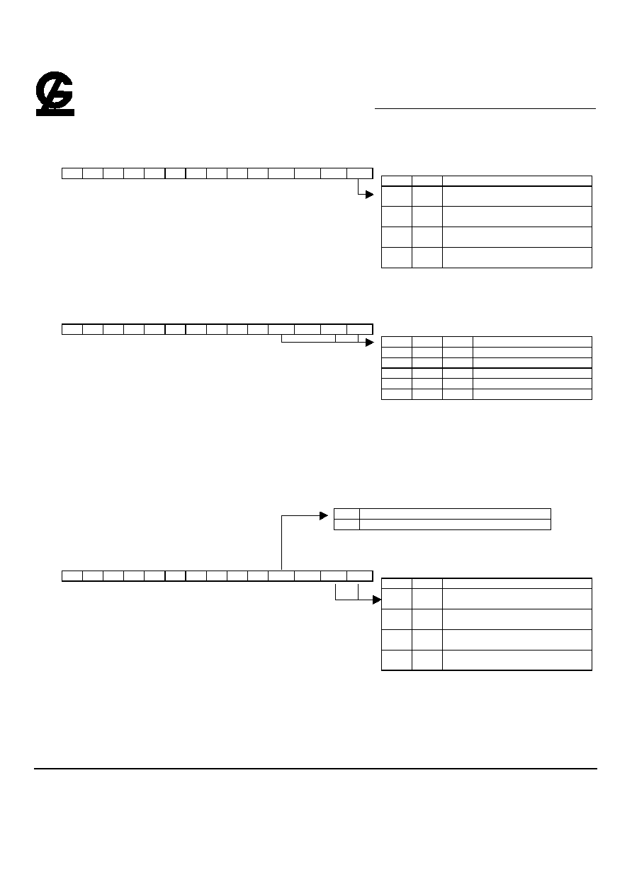
6.Address Bits of Bank-Select and Precharge
Row
A0
A1
A2
A3
A4
A5
A6
A7
A8
A9
A10
A11
BA1
BA0
(Activate command)
Row
A0
A1
A2
A3
A4
A5
A6
A7
A8
A9
A10
A11
BA1
BA0
(Precharge command)
Row
A0
A1
A2
A3
A4
A5
A6
A7
A8
A9
A10
A11
BA1
BA0
BA1
BA0
Result
0
0
Select Bank A
"Activate " command
0
1
Select Bank B
"Activate" command
1
0
Select Bank C
"Activate" command
1
1
Select Bank D
"Activate" command
A10
BA1
BA0
Result
0
0
0
Precharge Bank A
0
0
1
Precharge Bank B
0
1
0
Precharge Bank C
0
1
1
Precharge Bank D
1
X
X
Precharge All Banks
X : Don't care
BA1
BA0
Result
0
0
Enables Read/Write
commands for Bank A
0
1
Enables Read/Write
commands for Bank B
1
0
Enables Read/Write
commands for Bank C
1
1
Enables Read/Write
commands for Bank D
0
Disables Auto-Precharge (End of Burst)
1
Enables Auto - Precharge (End of Burst)
G -LINK
GLT5640AL16
4M X 16 CMOS Synchronous Dynamic RAM
Feb 2004 (Rev.0.1)
G-Link Technology Corporation, Taiwan
Web : www.glink.com.tw Email : sales@glink.com.tw
TEL : 886-2-27968078
- 19 -
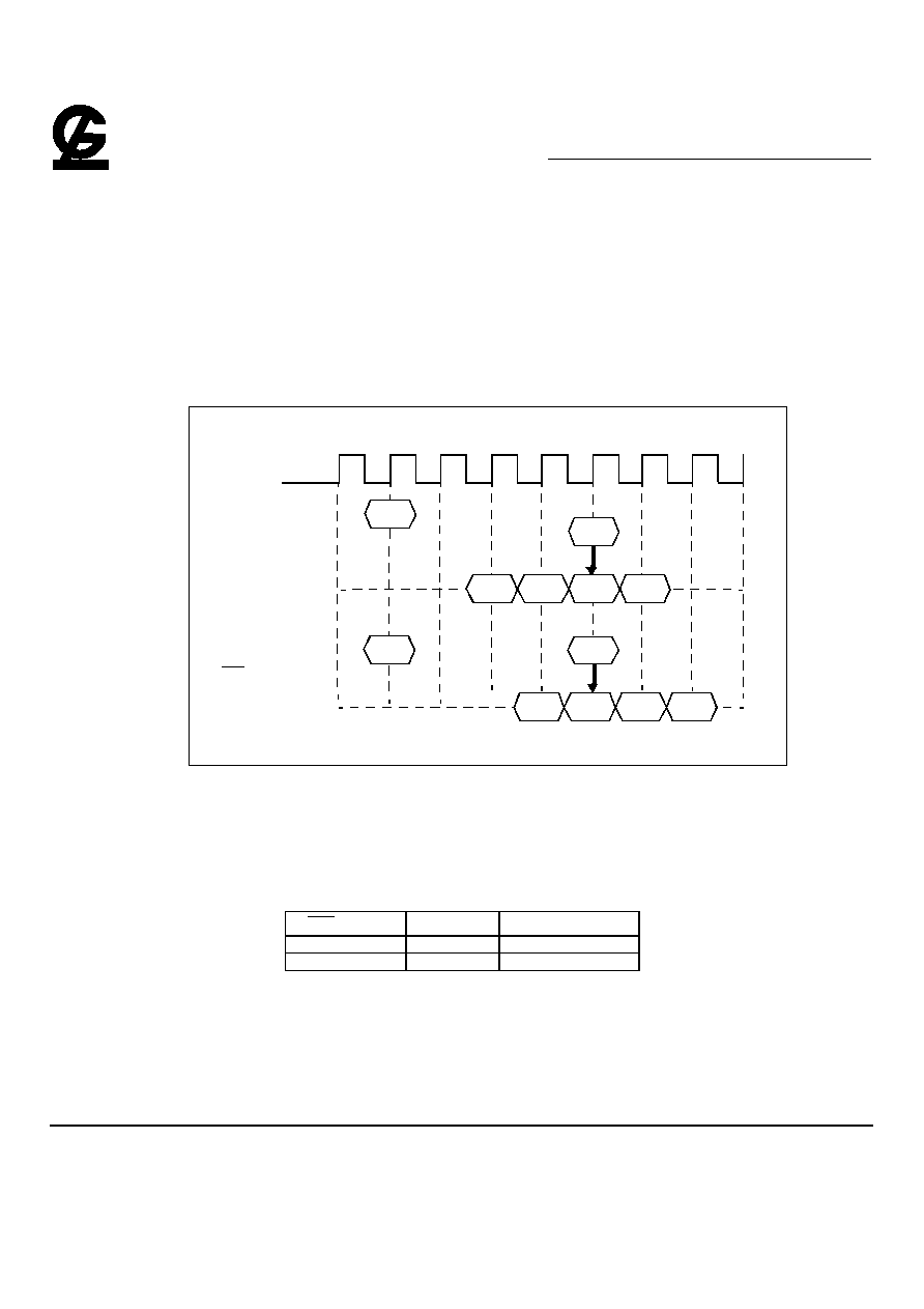
7.Precharge
The precharge command can be asserted anytime after t
RAS(min.)
is satisfied.
Soon after the precharge command is asserted, the precharge operation is performed and the synchronous DRAM enters the
idle state after t
RP(min.)
is satisfied. The parameter t
RP
is the time required to perform the precharge.
The earliest timing in a read cycle that a precharge command can be asserted without losing any data in the burst is as follows.
In order to write all data to the memory cell correctly, the asynchronous parameter "tDPL" must be satisfied. The tDPL(min.)
specification defines the earliest time that a precharge command can be asserted. The minimum number of clocks can be
calculated by dividing tDPL(min.) with the clock cycle time.
In summary, the precharge command can be asserted relative to the reference clock that indicates the last data word is valid.
In the following table, minus means clocks before the reference; plus means time after the reference.
CAS
latency
Read
Write
2
-1
+ t
DPL
(min.)
3
-2
+
tDPL
(min.)
Burst lengh=4
CLK
Command
CAS latency = 2
DQ
Command
CAS latency = 3
DQ
(t
R AS
is satisfied)
Hi - Z
Q0
Q3
Q2
Q1
PRE
Q0
Q3
Q2
Q1
Read
Read
T0
T1
T2
T3
T4
T5
T6
T7
PRE
Hi - Z
G -LINK
GLT5640AL16
4M X 16 CMOS Synchronous Dynamic RAM
Feb 2004 (Rev.0.1)
G-Link Technology Corporation, Taiwan
Web : www.glink.com.tw Email : sales@glink.com.tw
TEL : 886-2-27968078
- 20 -
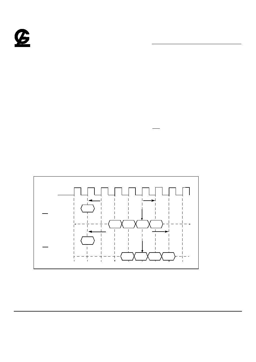
8.Auto Precharge
During a read or write command cycle, A10 controls whether auto precharge is selected. If A10 is high in the read or write
command (Read with Auto precharge command or Write with Auto precharge command), auto precharge is selected and begins
automatically.
In the write cycle, t
DAL
(min.) must be satisfied before asserting the next activate command to the bank being precharged.
When using auto precharge in the read cycle, knowing when the precharge starts is important because the next activate command
to the bank being precharged cannot be executed until the precharge cycle ends. Once auto precharge has started, an activate
command to the bank can be asserted after t
RP
has been satisfied.
A Read or Write command without auto - precharge can be terminated in the midst of a burst operation. However, a Read or
Write command with auto - precharge can not be interrupted by the same bank commands before the entire burst operation is
completed. Therefore use of the same bank Read, Write, Precharge or Burst Stop command is prohibited during a read or write
cycle with auto - precharge. It should be noted that the device will not respond to the Auto - Precharge command if the device is
programmed for full page burst read or write cycles.
The timing when the auto precharge cycle begins depends both on both the
CAS
Iatency programmed into the mode register
and whether the cycle is read or write.
8.1 Read with Auto Precharge
During a READA cycle, the auto precharge begins one clock earlier (CL = 2) or two clocks earlier (CL = 3) than the last word
output.
READ with AUTO PRECHARGE
Burst lengh = 4
CLK
Command
CAS l atency = 2
DQ
Command
CAS l atency = 3
DQ
Remark READA means READ with AUTO PRECHARGE
Hi - Z
Auto precharge starts
QB0
QB3
QB2
QB1
R E A D A B
R E A D A B
T0
T1
T2
T3
T4
T5
T6
T7
Auto precharge starts
Hi - Z
T8
QB0
QB3
QB2
QB1
No New Command to Bank B
No New Command to Bank B
G -LINK
GLT5640AL16
4M X 16 CMOS Synchronous Dynamic RAM
Feb 2004 (Rev.0.1)
G-Link Technology Corporation, Taiwan
Web : www.glink.com.tw Email : sales@glink.com.tw
TEL : 886-2-27968078
- 21 -
8.2 Write with Auto Precharge
During a write cycle, the auto precharge starts at the timing that is equal to the value of t
DPL
(min.) after the last data word input
to the device.
WRITE with AUTO PRECHRGE
In summary, the auto precharge cycle begins relative to a reference clock that indicates the
last data word is valid.
In the table below, minus means clocks before the reference; plus means clocks after the
reference.
CAS
latency
Read
Write
2
-1
+ t
DPL
(min.)
3
-2
+ t
DPL
(min.)
Burst lengh = 4
CLK
Command
CAS latency = 2
DQ
Command
CAS latency = 3
DQ
Remark WRITA means WRITE with AUTO Precharge
Hi - Z
DB0
DB3
DB2
DB1
WRITA B
WRITA B
T0
T1
T
2
T3
T4
T5
T6
T7
Hi - Z_
T8
t
DPL
t
DPL
DB0
DB3
DB2
DB1
AUTO PRECHARGE starts
AUTO PRECHARGE starts
G -LINK
GLT5640AL16
4M X 16 CMOS Synchronous Dynamic RAM
Feb 2004 (Rev.0.1)
G-Link Technology Corporation, Taiwan
Web : www.glink.com.tw Email : sales@glink.com.tw
TEL : 886-2-27968078
- 22 -
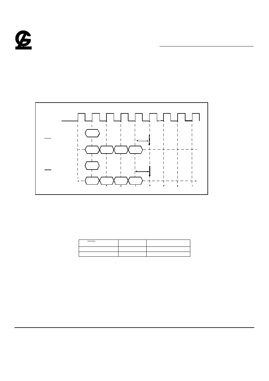
9. Read / Write Command Interval
9.1 Read to Read Command Interval
During a read cycle when a new read command is asserted, it will be effective after the
CAS
latency, even if the previous read
operation has not completed. READ will be interrupted by another READ.
Each read command can be asserted in every clock without any restriction.
READ to READ Command Interval
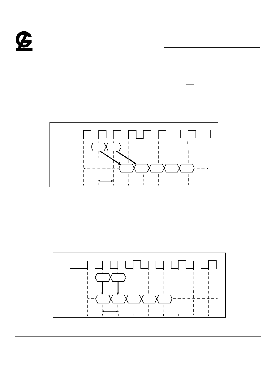
9.2 Write to Write Command Interval
During a write cycle, when a new Write command is asserted, the previous burst will terminated and the new burst will begin
with a new write command. WRITE will be interrupted by another WRITE.
Each write command can be asserted in every clock without any restriction.
WRITE to WRITE Command Interval
Burst lengh=4, C A S latency=2
CLK
Command
DQ
Q A0
QB2
QB1
QB0
Read A
T0
T1
T2
T3
T4
T5
T6
T7
Hi-Z_
T8
1 cycle
Q B3
Read B
Burst lengh=4, CAS latency=2
CLK
Command
DQ
QA0
QB2
QB1
Q B0
Write A
T0
T1
T2
T3
T4
T5
T6
T7
Hi-Z_
T8
1 cycle
Q B3
Write B
G -LINK
GLT5640AL16
4M X 16 CMOS Synchronous Dynamic RAM
Feb 2004 (Rev.0.1)
G-Link Technology Corporation, Taiwan
Web : www.glink.com.tw Email : sales@glink.com.tw
TEL : 886-2-27968078
- 23 -
9.3 Write to Read Command Interval
The write command to read command interval is also a minimum of 1 cycle. Only the write data before the read command will
be written. The data bus must be Hi-Z at least one cycle prior to the first DOUT.
WRITE to READ Command Interval
9.4 Read to Write Command Interval
During a read cycle, READ can be interrupted by WRITE.
DQM must be in High at least 3 clocks prior to the write command. There is a restriction to avoid a data conflict. The data bus
must be Hi-Z using DQM before Write.
Burst lengh=4
CLK
Command
CAS latency=2
DQ
Command
CAS latency=3
DQ
QB0
Q B3
Q B2
QB1
WRITE A
Write A
T0
T1
T2
T 3
T4
T5
T 6
T7
T8
QB0
QB3
Q B2
Q B1
1 cycle
Read B
DA0
Read B
DA0
Hi-Z
Hi-Z
G -LINK
GLT5640AL16
4M X 16 CMOS Synchronous Dynamic RAM
Feb 2004 (Rev.0.1)
G-Link Technology Corporation, Taiwan
Web : www.glink.com.tw Email : sales@glink.com.tw
TEL : 886-2-27968078
- 24 -
READ to WRITE Command Interval
CAS latency=2
CLK
Command
DQM
DQ
Hi-Z
D0
D3
D2
D1
Read
T0
T1
T2
T3
T4
T5
T6
T7
T8
1 cycle
Write
Burst length=8, CAS latency=2
CLK
C
omm
and
DQM
DQ
Q0
Read
T0
T1
T2
T3
T4
T5
T6
T7
T8
Write
T9
necessary
Q2
Q1
D0
D2
D1
Hi-Z is
example: Burst length=4, CAS
latency=3
CLK
Command
DQM
DQ
Read
T0
T1
T2
T3
T4
T5
T6
T7
T8
Write
necessary
D0
D2
D1
Hi-Z is
Q2
G -LINK
GLT5640AL16
4M X 16 CMOS Synchronous Dynamic RAM
Feb 2004 (Rev.0.1)
G-Link Technology Corporation, Taiwan
Web : www.glink.com.tw Email : sales@glink.com.tw
TEL : 886-2-27968078
- 25 -
10.BURST Termination
There are two methods to terminate a burst operation other than using a read or a write command. One is the burst stop
command and the other is the precharge command.
10.1 BURST Stop Command
During a read burst, when the burst stop command is issued, the burst read data are terminated and the data bus goes to high-
impedance after the
CAS
latency from the burst stop command.
During a write burst, when the burst stop command is issued, the burst write data are terminated and data bus goes to Hi-Z at
the same clock with the burst stop command.
Burst Termination
Remark BST: Burst stop command
Burst lengh=X, CAS Intency=2,3
CLK
Command
CAS latency=2
DQ
CAS latency=3
DQ
Q0
Q2
Q1
Read
T0
T1
T2
T3
T4
T5
T6
T7
BST
Hi-Z
Q0
Q2
Q1
Hi-Z
Burst lengh=X, CAS latency=2,3
CLK
Command
CAS latency=2,3
DQ
Q0
Q2
Q1
Write
T0
T1
T2
T3
T4
T5
T6
T7
BST
Hi-Z_
Q0
G -LINK
GLT5640AL16
4M X 16 CMOS Synchronous Dynamic RAM
Feb 2004 (Rev.0.1)
G-Link Technology Corporation, Taiwan
Web : www.glink.com.tw Email : sales@glink.com.tw
TEL : 886-2-27968078
- 26 -
10.2 PRECHARGE TERMINATION
10.2.1 PRECHARGE TERMINATION in READ Cycle
During READ cycle, the burst read operation is terminated by a precharge command.
When the precharge command is issued, the burst read operation is terminated and precharge starts.
The same bank can be activated again after t
RP
from the precharge command.
When
CAS
latency is 2, the read data will remain valid until one clock after the precharge command.
When
CAS
latency is 3, the read data will remain valid until two clocks after the precharge command.
Precharge Termination in READ Cycle
Burst lengh= X
CLK
Command
CAS latency=2
DQ
Hi-Z
Read
T0
T1
T2
T3
T4
T5
T6
T7
T8
PRE
ACT
DQ
Read
PRE
ACT
t
R P
C A S latency=3
Q0
Q3
Q2
Q1
Hi-Z
Q0
Q3
Q2
Q1
command
t
R P
G -LINK
GLT5640AL16
4M X 16 CMOS Synchronous Dynamic RAM
Feb 2004 (Rev.0.1)
G-Link Technology Corporation, Taiwan
Web : www.glink.com.tw Email : sales@glink.com.tw
TEL : 886-2-27968078
- 27 -
10.2.2 Precharge Termination in WRITE Cycle
During WRITE cycle, the burst write operation is terminated by a precharge command.
When the precharge command is issued, the burst write operation is terminated and precharge starts.
The same bank can be activated again after t
RP
from the precharge command. The DQM must be high to mask invalid data in.
During WRITE cycle, the write data written prior to the precharge command will be correctly stored. However, invalid data
may be written at the same clock as the precharge command. To prevent this from happening, DQM must be high at the same
clock as the precharge command. This will mask the invalid data.
PRECHARGE TERMINATION in WRITE Cycle
Burst lengh = X
CLK
Command
CAS latency = 2
DQM
Hi - Z
Write
T0
T1
T2
T3
T4
T5
T6
T7
T8
t
RP
PRE
ACT
DQ
Write
PRE
ACT
t
RP
CAS latency = 3
Hi - Z
D0
D3
D2
D1
D0
D3
D2
D1
DQM
D4
D4
command
DQ

G -LINK
GLT5640AL16
4M X 16 CMOS Synchronous Dynamic RAM
Feb 2004 (Rev.0.1)
G-Link Technology Corporation, Taiwan
Web : www.glink.com.tw Email : sales@glink.com.tw
TEL : 886-2-27968078
- 28 -
Timing Diagram
G -LINK
GLT5640AL16
4M X 16 CMOS Synchronous Dynamic RAM
Feb 2004 (Rev.0.1)
G-Link Technology Corporation, Taiwan
Web : www.glink.com.tw Email : sales@glink.com.tw
TEL : 886-2-27968078
- 29 -
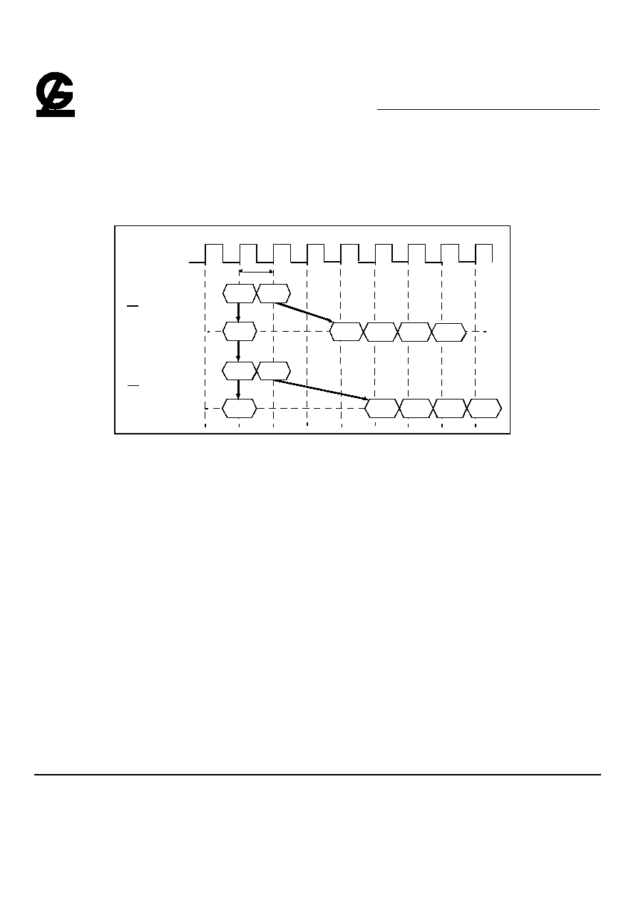
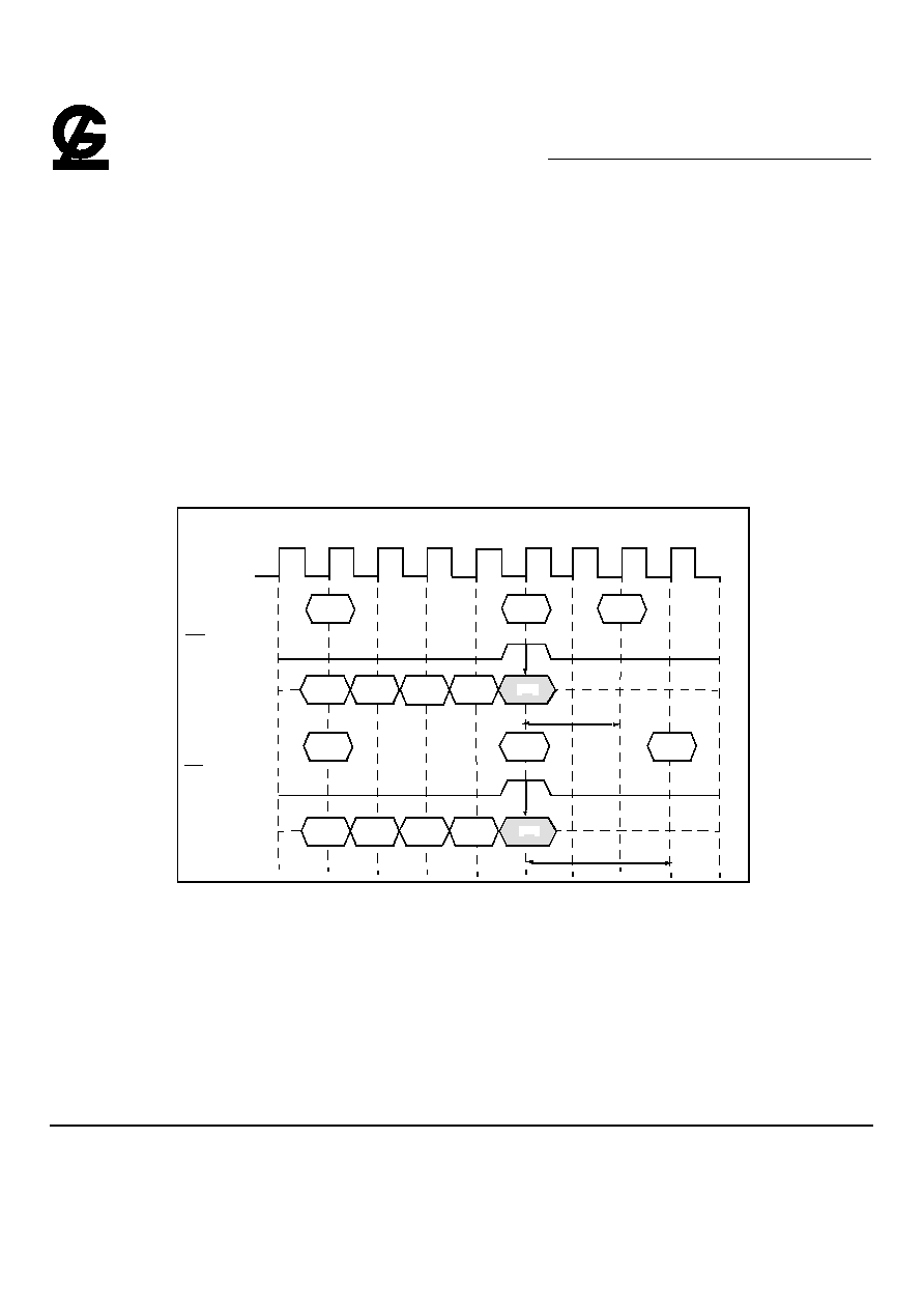
Mode Register Set
T0 T1 T2 T3 T4 T5 T6 T7 T8 T9 T1 0
CLK
CKE
CS
RAS
CAS
WE
BA0,1
A10
ADD
DQM
DQ
Command
Mode Register
Set
Command
All Banks
Precharge
Command
tRP
t
RSC
Hi-Z
Address Key
G -LINK
GLT5640AL16
4M X 16 CMOS Synchronous Dynamic RAM
Feb 2004 (Rev.0.1)
G-Link Technology Corporation, Taiwan
Web : www.glink.com.tw Email : sales@glink.com.tw
TEL : 886-2-27968078
- 30 -
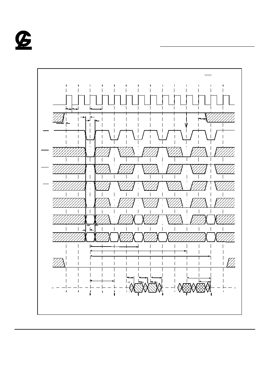
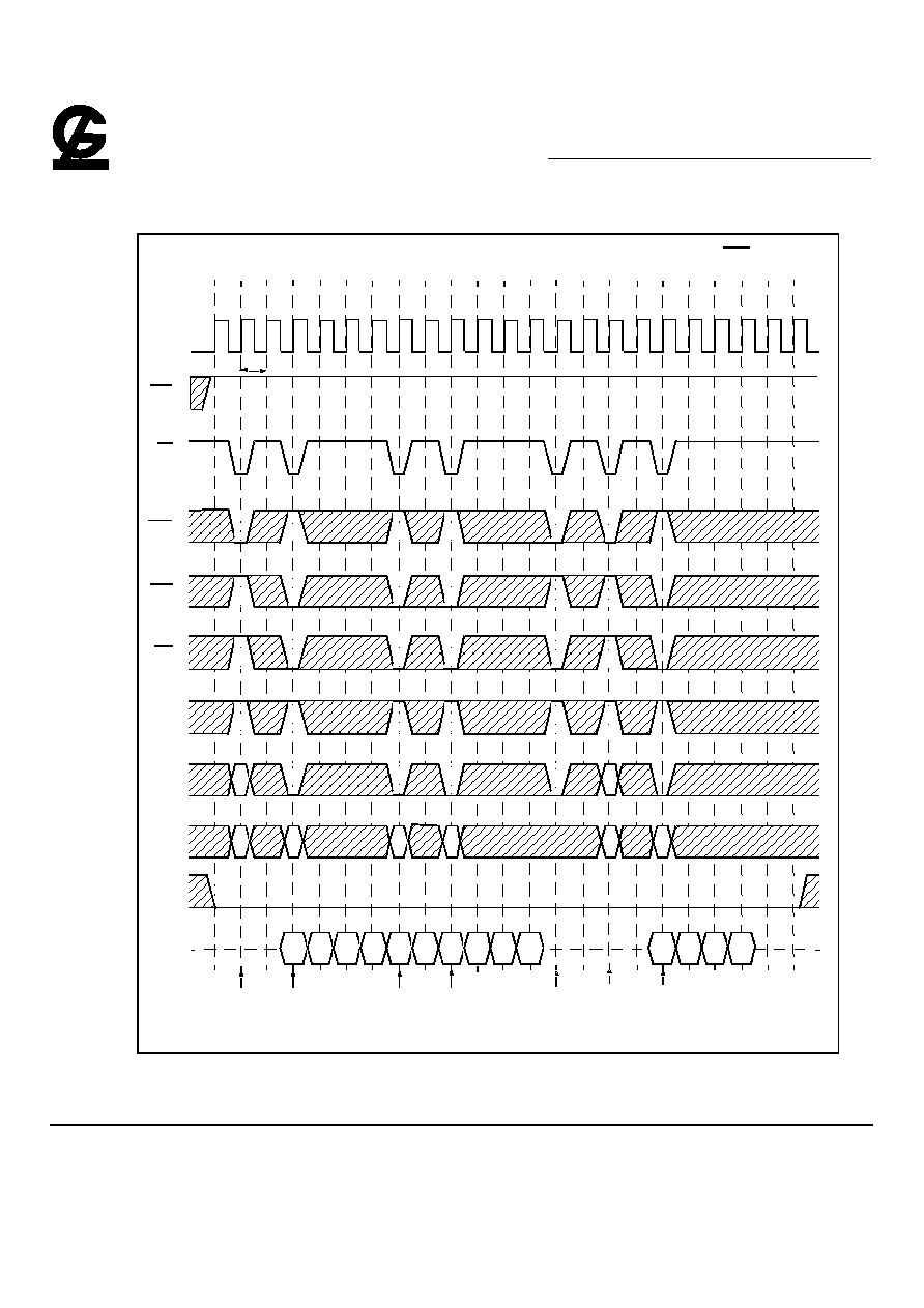
AC Parameters for Write Timing (1 of 2)
*BA1="L" , Bank C , D = Idle
T0 T1 T2 T3 T4 T5 T6 T7 T8 T9 T10 T11T12 T13 T14 T15 T16 T17 T18 T19 T20 T21 T22
tCH
t
CL
tCKS
t
CMS
t
CMH
tAS
t
AH
Begin Auto Precharge
Bank A
Begin Auto Precharge
Bank B
t
CKH
t
CK2
CLK
CKE
CS
RAS
CAS
WE
*BA0
A10
ADD
DQM
DQ
t
RCD
t
RRD
t
RC
t
DAL
QAa0 QAa1 QAa2 QAa3 QBa0 QBa1 QBa2 QBa3 QAb0 QAb1 QAb2 QAb3
Activate
Command
Bank A
Write with
Auto Precharge
Command
Bank A
Activate
Command
Bank B
Write with
Auto Precharge
Command
Bank B
Activate
Command
Bank A
Write without
Auto Precharge
Command
Bank A
t
DS
t
DH
t
DPL
RP
t
Precharge
Command
Bank A
Activate
Command
Bank A
Burst Length=4, CAS Latency=2
Activate
Command
Bank B
G -LINK
GLT5640AL16
4M X 16 CMOS Synchronous Dynamic RAM
Feb 2004 (Rev.0.1)
G-Link Technology Corporation, Taiwan
Web : www.glink.com.tw Email : sales@glink.com.tw
TEL : 886-2-27968078
- 31 -
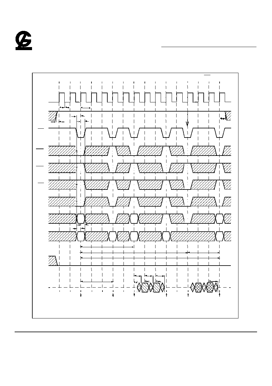
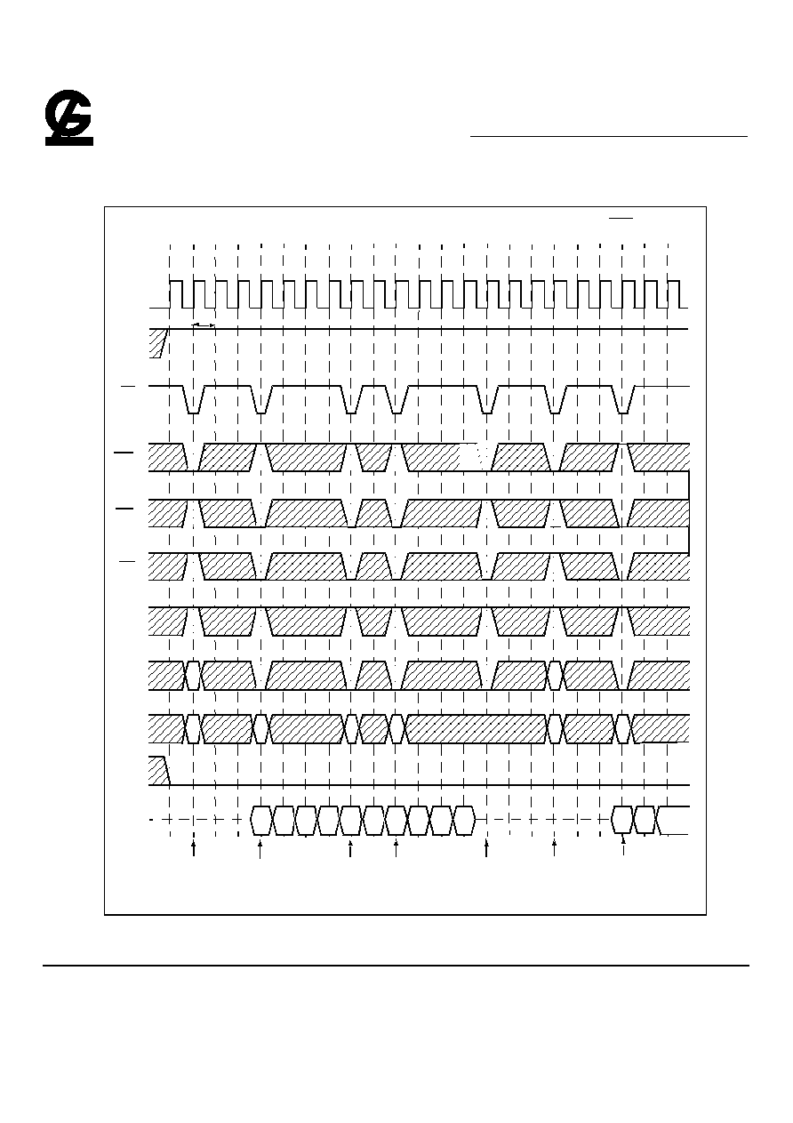
AC Parameters for Write Timing (2 of 2)
T0 T1 T2 T3 T4 T5 T6 T7 T8 T9 T10 T11 T12 T13 T14 T15 T16 T17 T18 T19 T20 T21 T22 T23
t
CH
t
CL
t
CKS
t
CMS
t
CMH
t
AS
t
AH
Begin Auto Precharge
Bank A
Begin Auto Precharge
Bank B
t
CKH
tCK3
CLK
CKE
CS
RAS
CAS
WE
A10
ADD
DQM
DQ
tRCD
t
RRD
RC
t
DAL
QAa0 QAa1 QAa2 QAa3 QBa0 QBa1 QBa2 QBa3
QAb0 QAb1 QAb2 QAb3
Activate
Command
Bank A
Write with
Auto Precharge
Command
Bank A
Activate
Command
Bank B
Write with
Auto Precharge
Command
Bank B
Activate
Command
Bank A
Write without
Auto Precharge
Command
Bank A
t
DS
t
DH
t
DPL
RP
t
Precharge
Command
Bank A
Activate
Command
Bank A
Burst Length=4, CAS Latency=3
*BA0

G -LINK
GLT5640AL16
4M X 16 CMOS Synchronous Dynamic RAM
Feb 2004 (Rev.0.1)
G-Link Technology Corporation, Taiwan
Web : www.glink.com.tw Email : sales@glink.com.tw
TEL : 886-2-27968078
- 32 -
*BA1="L" , Bank C , D = Idle
G -LINK
GLT5640AL16
4M X 16 CMOS Synchronous Dynamic RAM
Feb 2004 (Rev.0.1)
G-Link Technology Corporation, Taiwan
Web : www.glink.com.tw Email : sales@glink.com.tw
TEL : 886-2-27968078
- 33 -
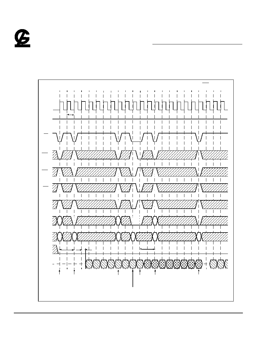
AC Parameters for Read Timing (1 of 2)
*BA1="L" , Bank C , D = Idle
T0 T1 T2 T3 T4 T5 T6 T7 T8 T9 T10 T11 T12 T13
CLK
CKE
CS
RAS
CAS
WE
A10
ADD
DQM
DQ
Burst Length=2, CAS Latency=2
tCH tCL
tCK2
Begin Auto
Precharge
Bank B
t
CKH
tCKS
t
CMS
tCMH
tAH
t
AS
tRRD
tRAS
t
RC
t
RCD
tAC2
tLZ
tOH
tAC2
tOH
tHZ
tRP
tHZ
Hi-Z
Activate
Command
Bank A
Read
Command
Bank A
Activate
Command
Bank B
Read with
Auto Precharge
Bank B
Precharge
Command
Bank A
Activate
Command
Bank A
QAa0
QAa1
QBa0
QBa1
Command
*BA0
G -LINK
GLT5640AL16
4M X 16 CMOS Synchronous Dynamic RAM
Feb 2004 (Rev.0.1)
G-Link Technology Corporation, Taiwan
Web : www.glink.com.tw Email : sales@glink.com.tw
TEL : 886-2-27968078
- 34 -
AC Parameters for Read Timing (2 of 2)
*BA1="L" , Bank C , D = Idle
T0 T1 T2 T3 T4 T5 T6 T7 T8 T9 T10 T11 T12 T13 T14 T15
CLK
CKE
CS
RAS
CAS
WE
A10
ADD
DQM
DQ
Burst Length=2, CAS Latency=3
tLZ
t
HZ
Hi-Z
Activate
Command
Bank A
Read
Command
Bank A
Activate
Command
Bank B
Read with
Auto Precharge
Bank B
Precharge
Command
Bank A
Activate
Command
Bank A
t
CH tCL
t
CKS
t
CK3
tCMS
tCMH
t
AH
t
AS
t
RRD
t
RAS
t
RC
t
RP
t
RCD
tAC3
tOH
t
AC3
QAa0
QAa1
QBa0
QBa1
tOH
tHZ
Command
t
CKH
Begin Auto
Precharge
Bank B
*BA0
G -LINK
GLT5640AL16
4M X 16 CMOS Synchronous Dynamic RAM
Feb 2004 (Rev.0.1)
G-Link Technology Corporation, Taiwan
Web : www.glink.com.tw Email : sales@glink.com.tw
TEL : 886-2-27968078
- 35 -
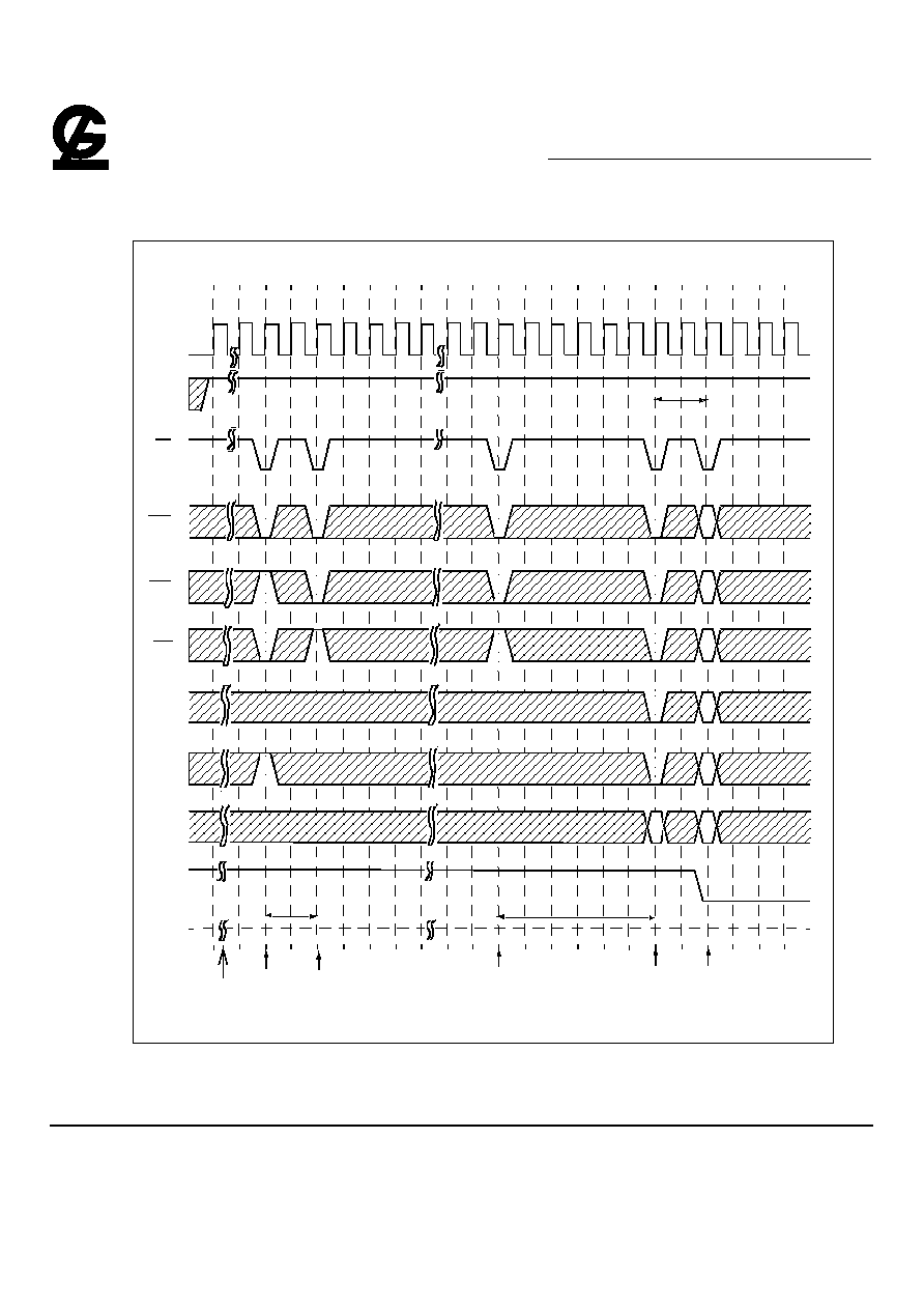
Power on Sequence and Auto Refresh (CBR)
T0 T1 T2 T3 T4 T5 T6 T7 T8 T9 T10 T11 T12 T13 T14 T15 T16 T17 T18 T19 T20 T21 T22
CLK
CKE
CS
RAS
CAS
WE
A10
ADD
DQM
DQ
High level
is required
Minimum of 8 Refresh Cycles are required
t
RSC
t
RP
High Level is Necessary
t
RC
Address Key
Inputs
be stable
for 200us
Precharge
All Banks
must
Command
1st Auto
Command
Refresh
2nd Auto
Refresh
Command
Mode
Set Command
Command
Register
Hi-Z
BA0, 1
G -LINK
GLT5640AL16
4M X 16 CMOS Synchronous Dynamic RAM
Feb 2004 (Rev.0.1)
G-Link Technology Corporation, Taiwan
Web : www.glink.com.tw Email : sales@glink.com.tw
TEL : 886-2-27968078
- 36 -
Clock Suspension During Burst Read (Using CKE)(1 of 2)
*BA1="L" , Bank C , D = Idle
T0 T1 T2 T3 T4 T5 T6 T7 T8 T9 T10 T11 T12 T13 T14 T15 T16 T17 T18 T19 T20 T21 T22
CLK
CKE
CS
RAS
CAS
WE
A10
ADD
DQM
DQ
t
HZ
Activate
Bank A
Command
Read
Bank A
Command
Clock
2 Cycles
Hi-Z
QAa0
QAa1
QAa2
QAa3
RAa
CAa
RAa
t
CK2
Clock
Suspended
1 Cycle
Suspended
Clock
3 Cycles
Suspended
Burst Length=4, CAS Latency=2
*BA0
G -LINK
GLT5640AL16
4M X 16 CMOS Synchronous Dynamic RAM
Feb 2004 (Rev.0.1)
G-Link Technology Corporation, Taiwan
Web : www.glink.com.tw Email : sales@glink.com.tw
TEL : 886-2-27968078
- 37 -
Clock Suspension During Burst Read (Using CKE)(2 of 2)
*BA1="L" , Bank C , D = Idle
T0 T1 T2 T3 T4 T5 T6 T7 T8 T9 T10 T11 T12 T13 T14 T15 T16 T17 T18 T19 T20 T21 T22
CLK
CKE
CS
RAS
C AS
WE
A10
ADD
DQM
DQ
t
HZ
Activate
Bank A
Command
Read
Bank A
Command
Clock
2 Cycles
Hi-Z
QAa0
QAa1
QAa2
QAa3
RAa
RAa
t
CK3
Clock
Suspended
1 Cycles
Suspended
Clock
3 Cycles
Suspended
Burst Length=4, CAS Latency=3
CAa
*BA0
G -LINK
GLT5640AL16
4M X 16 CMOS Synchronous Dynamic RAM
Feb 2004 (Rev.0.1)
G-Link Technology Corporation, Taiwan
Web : www.glink.com.tw Email : sales@glink.com.tw
TEL : 886-2-27968078
- 38 -
Clock Suspension During Burst Write (Using CKE)(1 of 2)
*BA1="L" , Bank C , D = Idle
T0 T1 T2 T3 T4 T5 T6 T7 T8 T9 T10 T11 T12 T13 T14 T15 T16 T17 T18 T19 T20 T21 T22
CLK
CKE
CS
RAS
CAS
WE
A10
ADD
DQM
DQ
Activate
Bank A
Command
Write
Bank A
Command
Clock
2 Cycles
Hi-Z
RAa
CAa
RAa
t
CK2
Clock
Suspended
1 Cycle
Suspended
Clock
3 Cycles
Suspended
Burst Length=4, CAS Latency=2
DAa0
DAa1
DAa2
DAa3
*BA0
G -LINK
GLT5640AL16
4M X 16 CMOS Synchronous Dynamic RAM
Feb 2004 (Rev.0.1)
G-Link Technology Corporation, Taiwan
Web : www.glink.com.tw Email : sales@glink.com.tw
TEL : 886-2-27968078
- 39 -
Clock Suspension During Burst Write (Using CKE)(2 of 2)
*BA1="L" , Bank C , D = Idle
T0 T1 T2 T3 T4 T5 T6 T7 T8 T9 T10 T11 T12 T13 T14 T15 T16 T17 T18 T19 T20 T21 T22
CLK
CKE
CS
RAS
CAS
WE
A10
ADD
DQM
DQ
RAa
RAa
t
CK3
Burst Length=4, CAS Latency=3
CAa
Activate
Bank A
Command
Write
Bank A
Command
Clock
2 Cycles
Hi-Z
Clock
Suspended
1 Cycle
Suspended
Clock
3 Cycles
Suspended
DAa0
DAa1
DAa2
DAa3
*BA0
G -LINK
GLT5640AL16
4M X 16 CMOS Synchronous Dynamic RAM
Feb 2004 (Rev.0.1)
G-Link Technology Corporation, Taiwan
Web : www.glink.com.tw Email : sales@glink.com.tw
TEL : 886-2-27968078
- 40 -
Power Down Mode and Clock Mask
*BA1="L" , Bank C , D = Idle
T0 T1 T2 T3 T4 T5 T6 T7 T8 T9 T10 T11 T12 T13 T14 T15 T16 T17 T18 T19 T20 T21 T22
CLK
CKE
CS
RAS
CAS
WE
A10
ADD
DQM
DQ
RAa
RAa
t
CK2
Burst Length=4, CAS Latency=2
Activate
Bank A
Command
Power Down
Mode Entry
Power Down
Bank A
Hi-Z
ACTIVE
STANDBY
Read
Clock Mask
CAa
t
CKS
t
CKH
VALID
t
CKS
RAa
QAa0 QAa1
QAa2
Mode Exit
Command
Start
Clock Mask
End
Precharge
Command
Power Down
Mode Entry
Precharge
Standby
Power
Mode
Down
Exit
Command
*BA0
QAa3
G -LINK
GLT5640AL16
4M X 16 CMOS Synchronous Dynamic RAM
Feb 2004 (Rev.0.1)
G-Link Technology Corporation, Taiwan
Web : www.glink.com.tw Email : sales@glink.com.tw
TEL : 886-2-27968078
- 41 -
Auto Refresh (CBR)
*BA1="L" , Bank C , D = Idle
T0 T1 T2 T3 T4 T5 T6 T7 T8 T9 T10 T11 T12 T13 T14 T15 T16 T17 T18 T19 T20 T21 T22
CLK
CKE
CS
RAS
CAS
WE
A10
ADD
DQM
DQ
t
CK2
Burst Length=4, CAS Latency=2
Precharge
All Banks
Command
CBR Refresh
Hi-Z
CBR Refresh
Command
Activate
Command
Read
RAa
CAa
RAa
Q0
Q1
Q2
Q3
Command
Command
t
RP
t
RC
t
RC
*BA0, 1
G -LINK
GLT5640AL16
4M X 16 CMOS Synchronous Dynamic RAM
Feb 2004 (Rev.0.1)
G-Link Technology Corporation, Taiwan
Web : www.glink.com.tw Email : sales@glink.com.tw
TEL : 886-2-27968078
- 42 -
Self Refresh (Entry and Exit)
*BA1="L" , Bank C , D = Idle
*Clock can be stopped at CKE=Low. If clock is stopped, it must be restarted/stable for 4 clock cycles before
CKE=High
T0 T1 T2 T3 T4 T5 T6 T7 T8 T9 T10 T11 T12 T13 T14 T15 T16 T17 T18 T19 T20 T21 T22
CLK
CKE
CS
RAS
CAS
WE
A10
ADD
DQM
DQ
t
SRX
All Banks
Self refresh
Hi-Z
Self Refresh
Exit
Self Refresh
Entry
Exit
t
RC
t
CKS
t
SRX
t
CKS
t
RC
must be idle
Self Refresh
Entry
Activate
Command
CLK can be Stopped
**
*BA0
G -LINK
GLT5640AL16
4M X 16 CMOS Synchronous Dynamic RAM
Feb 2004 (Rev.0.1)
G-Link Technology Corporation, Taiwan
Web : www.glink.com.tw Email : sales@glink.com.tw
TEL : 886-2-27968078
- 43 -
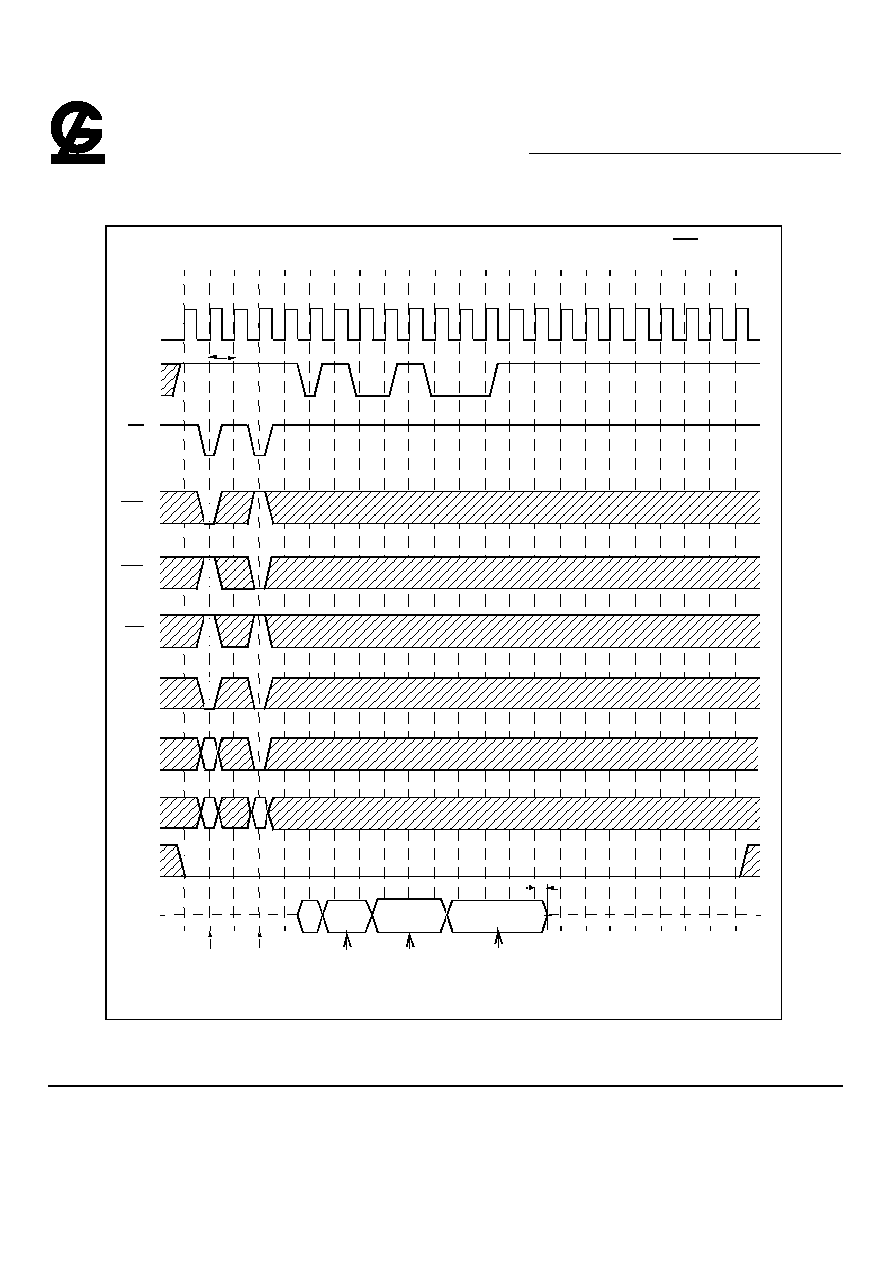
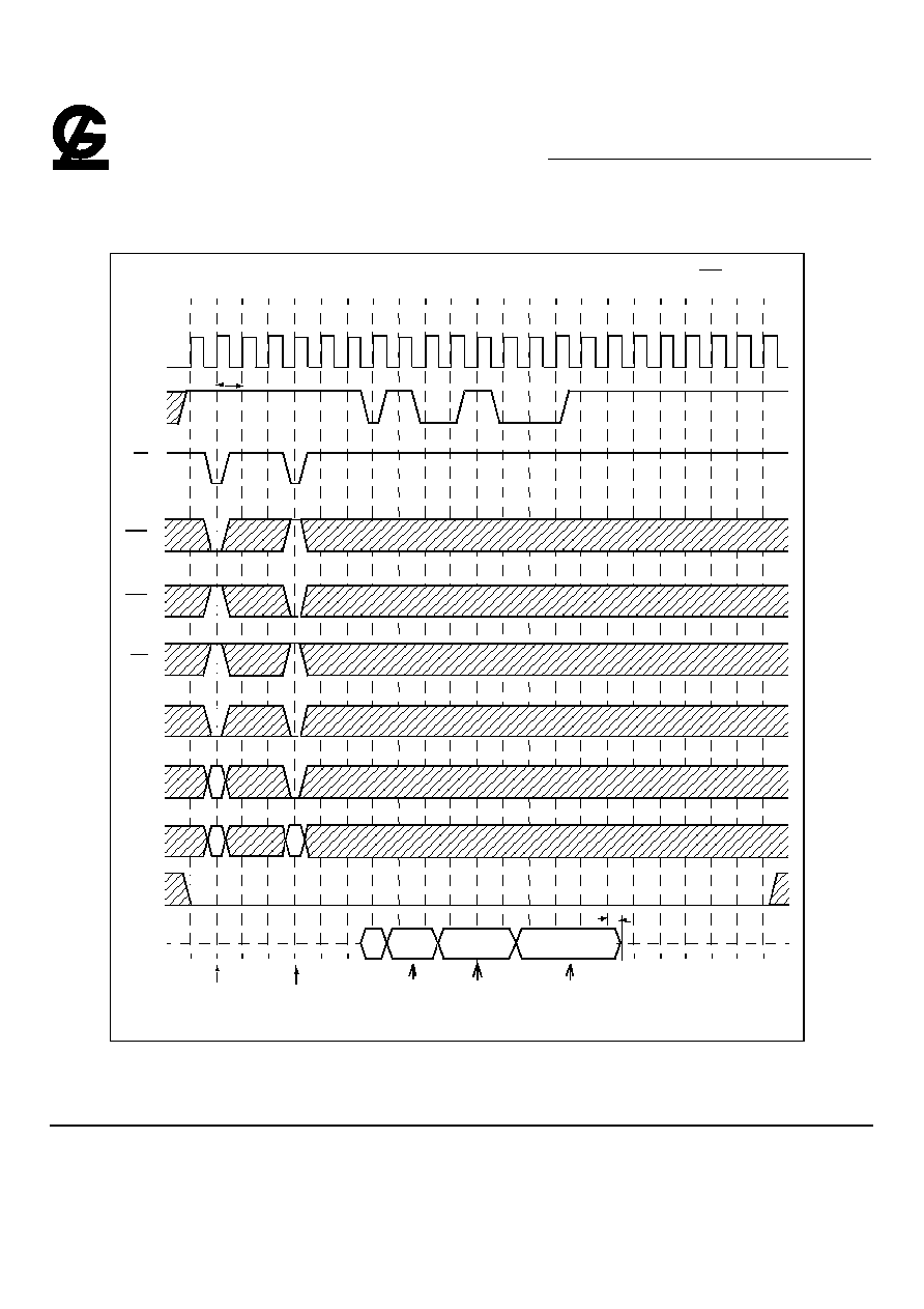
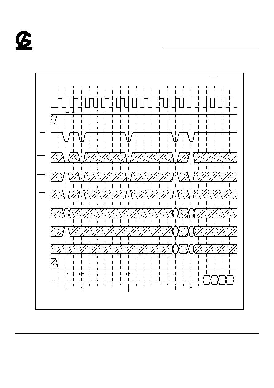
Random Column Read (Page With Same Bank)(1 of 2)
*BA1="L" , Bank C , D = Idle
T0 T1 T2 T3 T4 T5 T6 T7 T8 T9 T10 T11 T12 T13 T14 T15 T16 T17 T18 T19 T20 T21 T22
CLK
CKE
CS
RAS
CAS
WE
A10
ADD
DQM
DQ
t
CK2
Burst Length=4, CAS Latency=2
Precharge
Bank A
Command
Read
Hi-Z
Activate
Read
RAa
QAd0
Command
Command
RAa
CAa
RAa
CAb
CAc
RAd
RAd
CAd
QAa0 QAa1 QAa2 QAa3 QAb0 QAb1 QAc0 QAc1 QAc2 QAc3
QAd1 QAd2 QAd3
Bank A
Read
Command
Bank A
Read
Command
Bank A
Precharge
Command
Bank A
Bank A
Command
Bank A
*BA0
G -LINK
GLT5640AL16
4M X 16 CMOS Synchronous Dynamic RAM
Feb 2004 (Rev.0.1)
G-Link Technology Corporation, Taiwan
Web : www.glink.com.tw Email : sales@glink.com.tw
TEL : 886-2-27968078
- 44 -
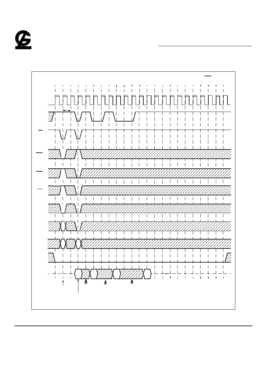
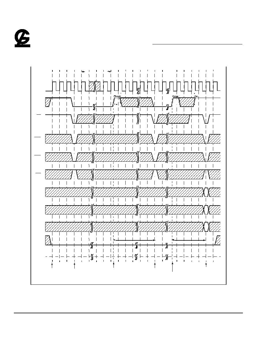
Random Column Read (Page With Same Bank)(2 of 2)
*BA1="L" , Bank C , D = Idle
T0 T1 T2 T3 T4 T5 T6 T7 T8 T9 T10 T11 T12 13 T14 T15 T16 T17 T18 T19 T20 T21 T22
CLK
CKE
CS
RAS
CAS
WE
A10
ADD
DQM
DQ
t
CK3
Burst Length=4, CAS Latency=3
Activate
Bank A
Command
Read
Hi-Z
Activate
Read
Command
Command
RAa
CAa
CAb
CAc
RAd
CAd
QAc2 QAc3
QAa0 QAa1 QAa2 QAa3 QAb0 QAb1 QAc0 QAc1
Bank A
Read
Command
Bank A
Precharge
Command
Bank A
Bank A
Command
Bank A
RAd
Read
Command
Bank A
RAa
*BA0
G -LINK
GLT5640AL16
4M X 16 CMOS Synchronous Dynamic RAM
Feb 2004 (Rev.0.1)
G-Link Technology Corporation, Taiwan
Web : www.glink.com.tw Email : sales@glink.com.tw
TEL : 886-2-27968078
- 45 -
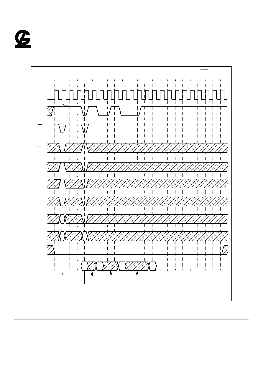
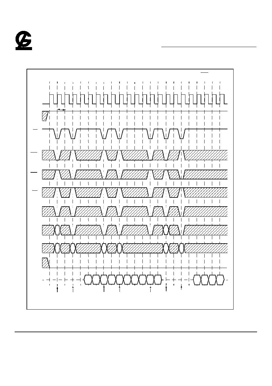
Random Column Write (Page With Same Bank)(1 of 2)
*BA1="L" , Bank C , D = Idle
T0 T1 T2 T3 T4 T5 T6 T7 T8 T9 T10 T11 T12 T13 T14 T15 T16 T17 T18 T19 T20 T21 T22
CLK
CKE
CS
RAS
CAS
WE
A10
ADD
DQM
DQ
t
CK2
Burst Length=4, CAS Latency=2
Activate
Bank B
Command
Write
Hi-Z
Activate
Write
Command
Command
Ra
Ca
Ra
Cb
Cc
Rd
Cd
Dc2 Dc3
Da1 Da2
Da3
Db0 Db1 Dc0 Dc1
Bank B
Write
Command
Bank B
Precharge
Command
Bank B
Bank B
Command
Bank B
Write
Command
Bank B
Rd
Dd2 Dd3
Dd0 Dd1
Da0
*BA0
G -LINK
GLT5640AL16
4M X 16 CMOS Synchronous Dynamic RAM
Feb 2004 (Rev.0.1)
G-Link Technology Corporation, Taiwan
Web : www.glink.com.tw Email : sales@glink.com.tw
TEL : 886-2-27968078
- 46 -
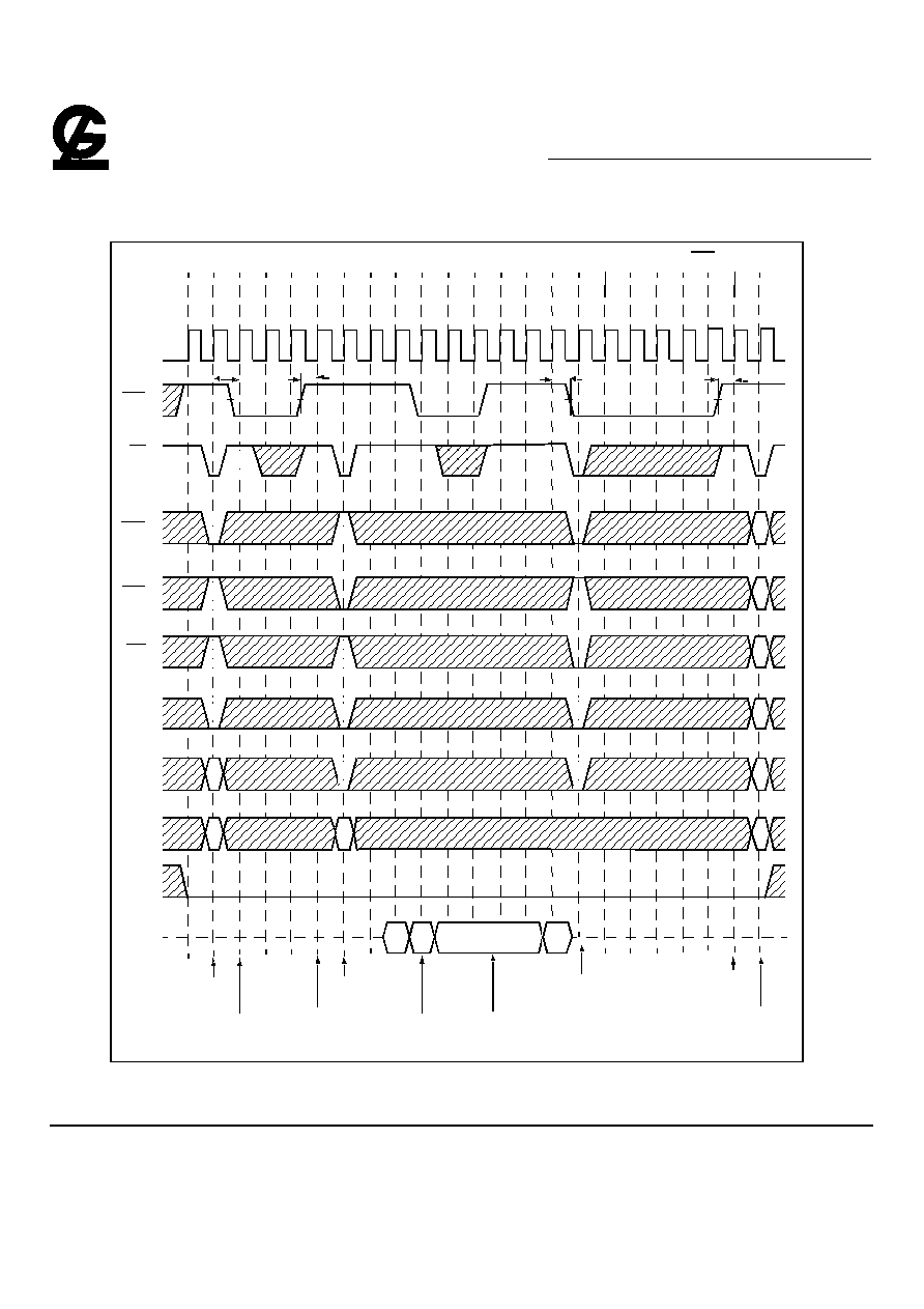
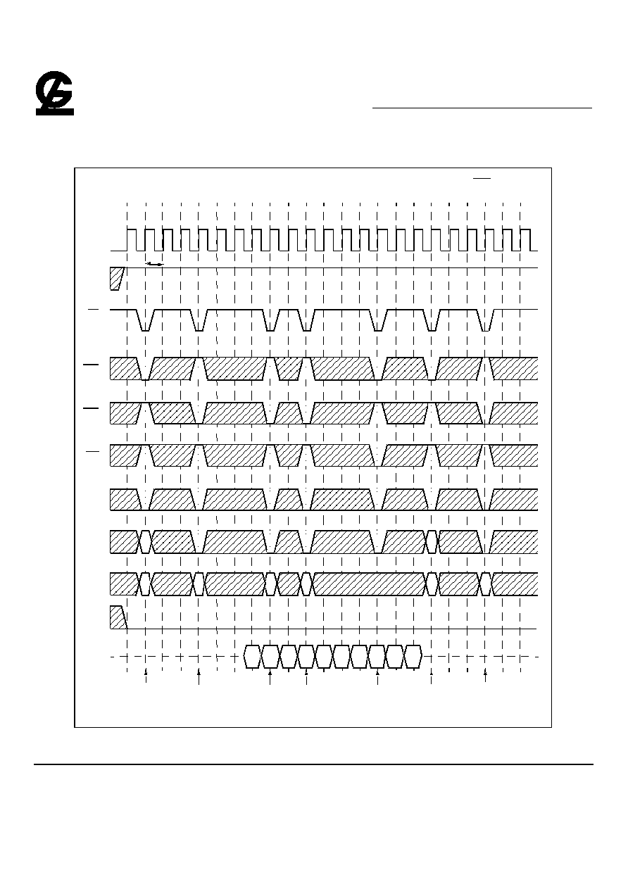
Random Column Write (Page With Same Bank)(2 of 2)
*BA1="L" , Bank C , D = Idle
T0 T1 T2 T3 T4 T5 T6 T7 T8 T9 T10 T11 T12 T13 T14 T15 T16 T17 T18 T19 T20 T21 T22
CLK
CKE
CS
RAS
CAS
WE
A10
ADD
DQM
DQ
t
CK
Burst Length=4, CAS Latency=3
Activate
Bank B
Command
Write
Hi-Z
Activate
Command
Ra
Ca
Ra
Cb
Cc
Cd
Rd
Bank B
Write
Command
Bank B
Precharge
Command
Bank B
Command
Bank B
Write
Command
Bank B
Rd
Write
Command
Bank B
Dc2
Dc3
Da1
Da2 Da3
Db0 Db1
Dc0
Dc1
Da0
Dd0
Dd1
*BA0
G -LINK
GLT5640AL16
4M X 16 CMOS Synchronous Dynamic RAM
Feb 2004 (Rev.0.1)
G-Link Technology Corporation, Taiwan
Web : www.glink.com.tw Email : sales@glink.com.tw
TEL : 886-2-27968078
- 47 -
Random Row Read (Interleaving Banks)(1 of 2)
*BA1="L" , Bank C , D = Idle
T0 T1 T2 T3 T4 T5 T6 T7 T8 T9 T10 T11 T12 T13 T14 T15 T16 T17 T18 T19 T20 T21 T22
CLK
CKE
CS
RAS
CAS
WE
A10
ADD
DQM
DQ
t
CK2
Burst Length=8, CAS Latency=2
Activate
Bank B
Command
Read
Hi-Z
Command
QAa0
QAa1
QBa1 QBa2 QBa3 QBa4 QBa5 QBa6
QBa7
Bank B
Activate
Command
Bank A
Active
Command
Bank B
Read
Command
Bank A
QBb1
QBb0
QBa0
Read
Command
Bank B
QAa3 QAa4 QAa5 QAa6
QAa7
QAa2
Precharge
Command
Bank B
t
RCD
t
AC2
t
RP
High
*BA0
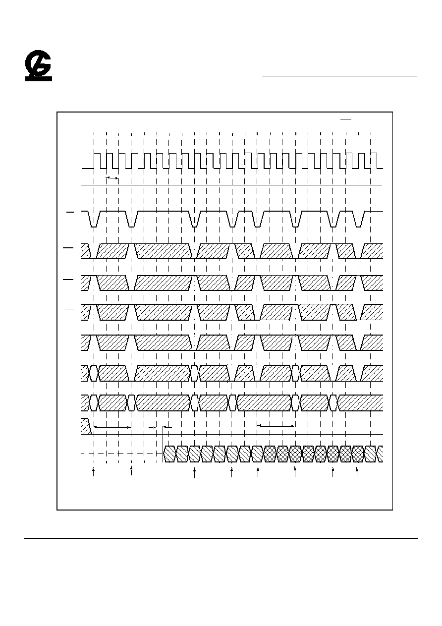
G -LINK
GLT5640AL16
4M X 16 CMOS Synchronous Dynamic RAM
Feb 2004 (Rev.0.1)
G-Link Technology Corporation, Taiwan
Web : www.glink.com.tw Email : sales@glink.com.tw
TEL : 886-2-27968078
- 48 -
Random Row Read (Interleaving Banks)(2 of 2)
*BA1="L" , Bank C , D = Idle
T0 T1 T2 T3 T4 T5 T6 T7 T8 T9 T10 T11 T12 T13 T14 T15 T16 T17 T18 T19 T20 T21 T22
CLK
CKE
CS
RAS
CAS
WE
A10
ADD
DQM
DQ
t
CK3
Burs Length=8, CAS Latency=3
Activate
Bank B
Command
Read
Hi-Z
Command
QAa0 QAa1
QBa1 QBa2 QBa3 QBa4 QBa5 QBa6 QBa7
Bank B
Activate
Command
Bank A
Precharge
Command
Bank B
QBb0
QBa0
Read
Command
Bank B
QAa3 QAa4 QAa5QAa6 QAa7
QAa2
Read
Command
Bank A
t
RCD
t
AC3
t
RP
High
Activate
Bank B
Command
Precharge
Command
Bank A
*BA0
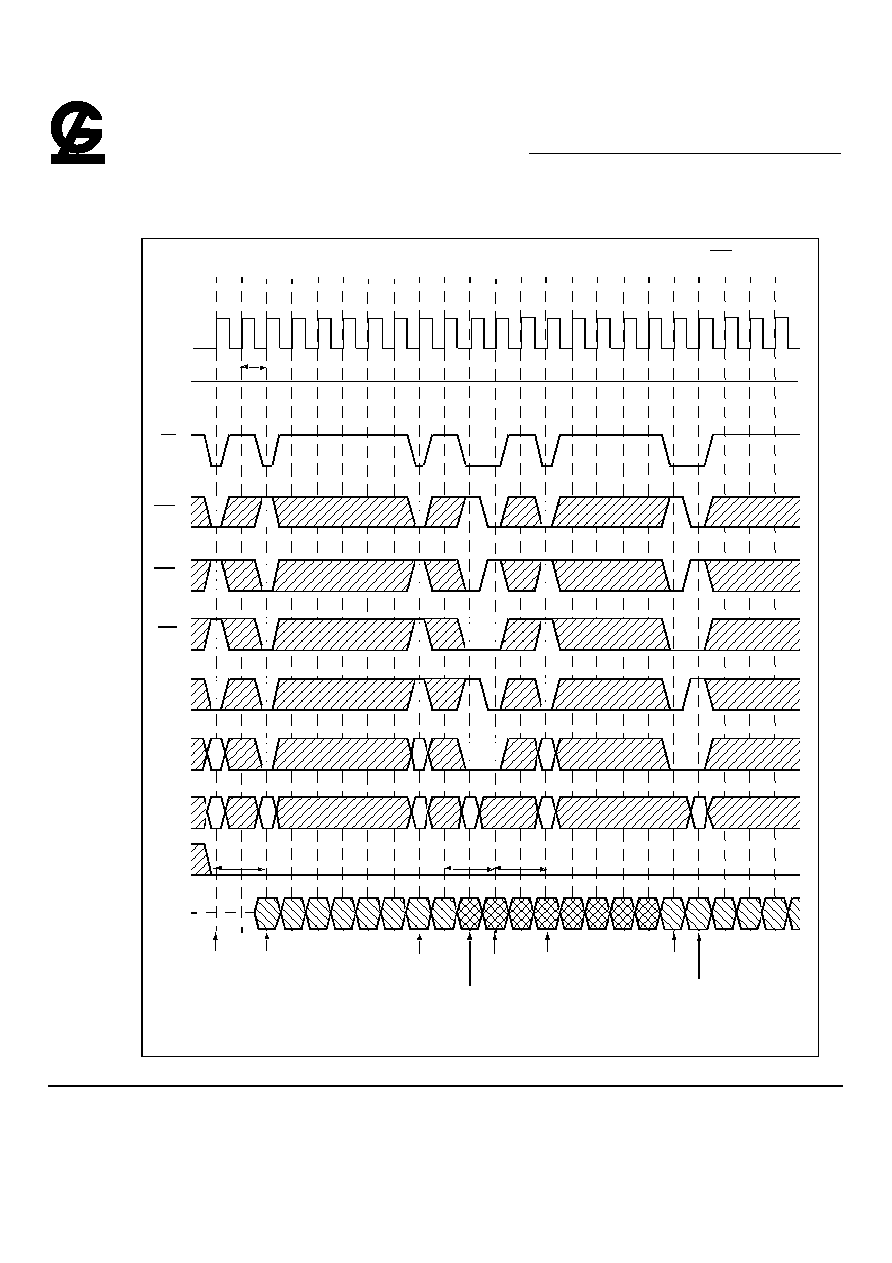
G -LINK
GLT5640AL16
4M X 16 CMOS Synchronous Dynamic RAM
Feb 2004 (Rev.0.1)
G-Link Technology Corporation, Taiwan
Web : www.glink.com.tw Email : sales@glink.com.tw
TEL : 886-2-27968078
- 49 -
Random Row Write (Interleaving Banks)(1 of 2)
*BA1="L" , Bank C , D = Idle
T0 T1 T2 T3 T4 T5 T6 T7 T8 T9 T10 T11 T12 T13 T14 T15 T16 T17 T18 T19 T20 T21 T22
CLK
CKE
CS
RAS
CAS
WE
A10
ADD
DQM
DQ
t
CK2
Burst Length=8, CAS Latency=2
Activate
Bank A
Command
Write
Hi-Z
Command
QBa0 QBa1
QAa1
QAa2 QAa3 QAa4 QAa5 QAa6 QAa7
Bank A
Activate
Command
Bank B
Active
Command
Bank A
Write
Command
Bank B
QAb3
QAb2
QAa0
Write
Command
Bank A
QBa3
QBa4 QBa5 QBa6 QBa7
QBa2
Precharge
Command
Bank A
t
RCD
t
RP
High
t
DPL
QAb0 QAb1
QAb4
Precharge
Command
Bank B
*BA0
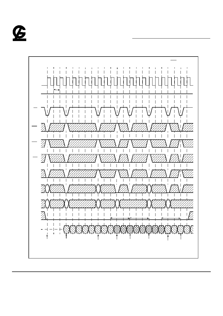
G -LINK
GLT5640AL16
4M X 16 CMOS Synchronous Dynamic RAM
Feb 2004 (Rev.0.1)
G-Link Technology Corporation, Taiwan
Web : www.glink.com.tw Email : sales@glink.com.tw
TEL : 886-2-27968078
- 50 -
Random Row Write (Interleaving Banks)(2 of 2)
*BA1="L" , Bank C , D = Idle
T0 T1 T2 T3 T4 T5 T6 T7 T8 T9 T10 T11 T12 T13 T14 T15 T16 T17 T18 T19 T20 T21 T22
CLK
CKE
CS
RAS
CAS
WE
A10
ADD
DQM
DQ
t
CK
Burst Length=8, CAS Latency=3
Activate
Bank A
Command
Write
Hi-Z
Command
QAa7 QBa0
QAa0 QAa1 QAa2QAa3 QAa4 QAa5 QAa6
Bank A
Activate
Command
Bank B
QAb2
QAb1
Activate
Command
Bank A
QBa2 QBa3QBa4 QBa5 QBa6
QBa1
Write
Command
Bank B
RBa
t
RP
High
t
DPL
t
DPL
QBb7QAb0
QAb3
Write
Command
Bank A
Precharge
Command
Bank A
Precharge
Command
Bank B
*BA0
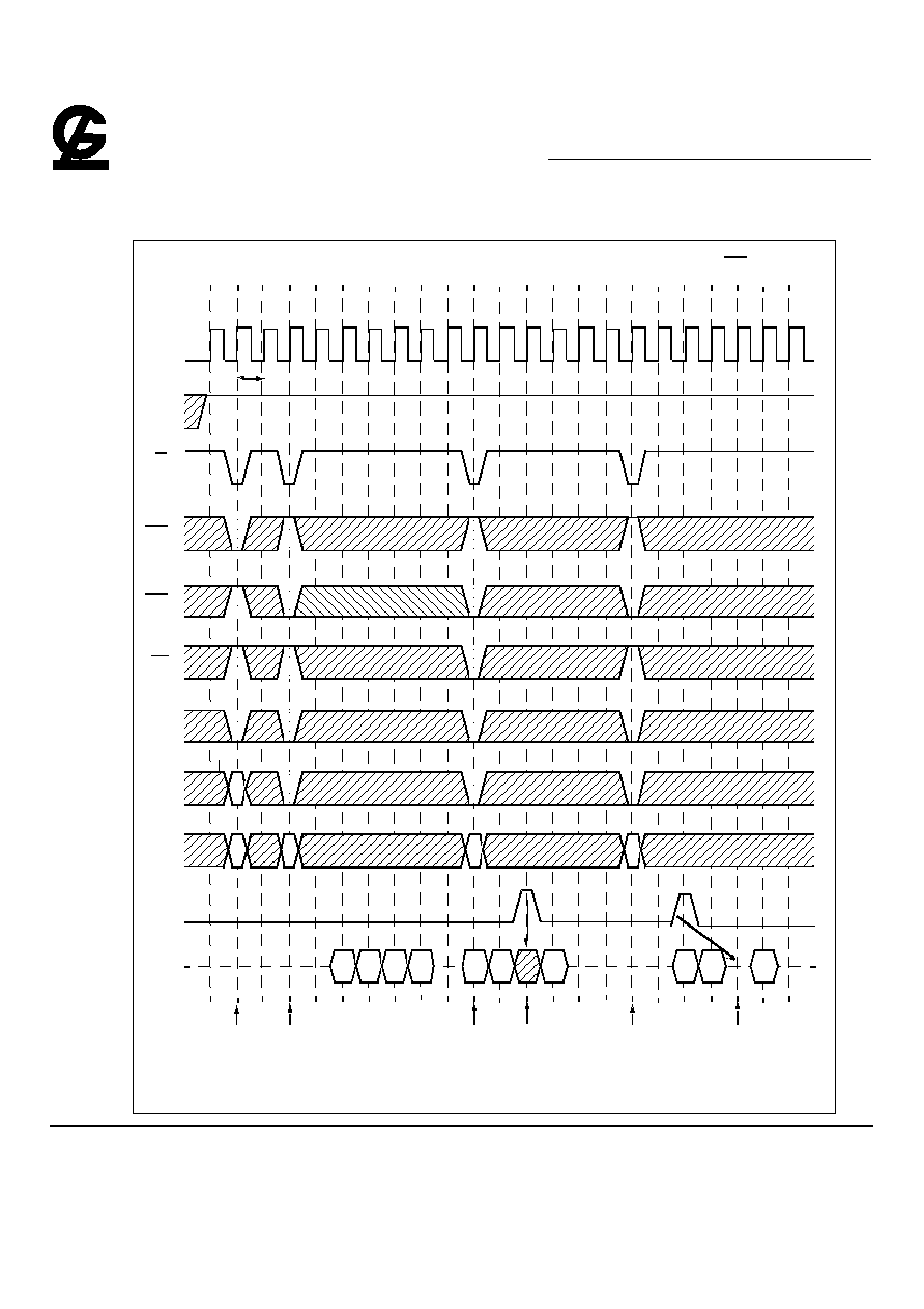
G -LINK
GLT5640AL16
4M X 16 CMOS Synchronous Dynamic RAM
Feb 2004 (Rev.0.1)
G-Link Technology Corporation, Taiwan
Web : www.glink.com.tw Email : sales@glink.com.tw
TEL : 886-2-27968078
- 51 -
Read and Write Cycle (1 of 2)
*BA1="L" , Bank C , D = Idle
T0 T1 T2 T3 T4 T5 T6 T7 T8 T9 T10 T11 T12 T13 T14 T15 T16 T17 T18 T19 T20 T21 T22
CLK
CKE
CS
RAS
CAS
WE
A10
ADD
DQM
DQ
t
CK2
Burst Length=4, CAS Latency=2
Activate
Bank A
Command
Write
Hi-Z
Command
DAb3
QAc0
QAa0 QAa1 QAa2QAa3
DAb0 DAb1
Bank A
Write
Command
Bank A
Read
Command
Bank A
QAc3
QAc1
The Read Data
The Write Data
is Masked with a
Zero Clock
RAa
RAa
CAb
CAc
CAa
latency
is Masked with
Two Clocks
Latency
*BA0
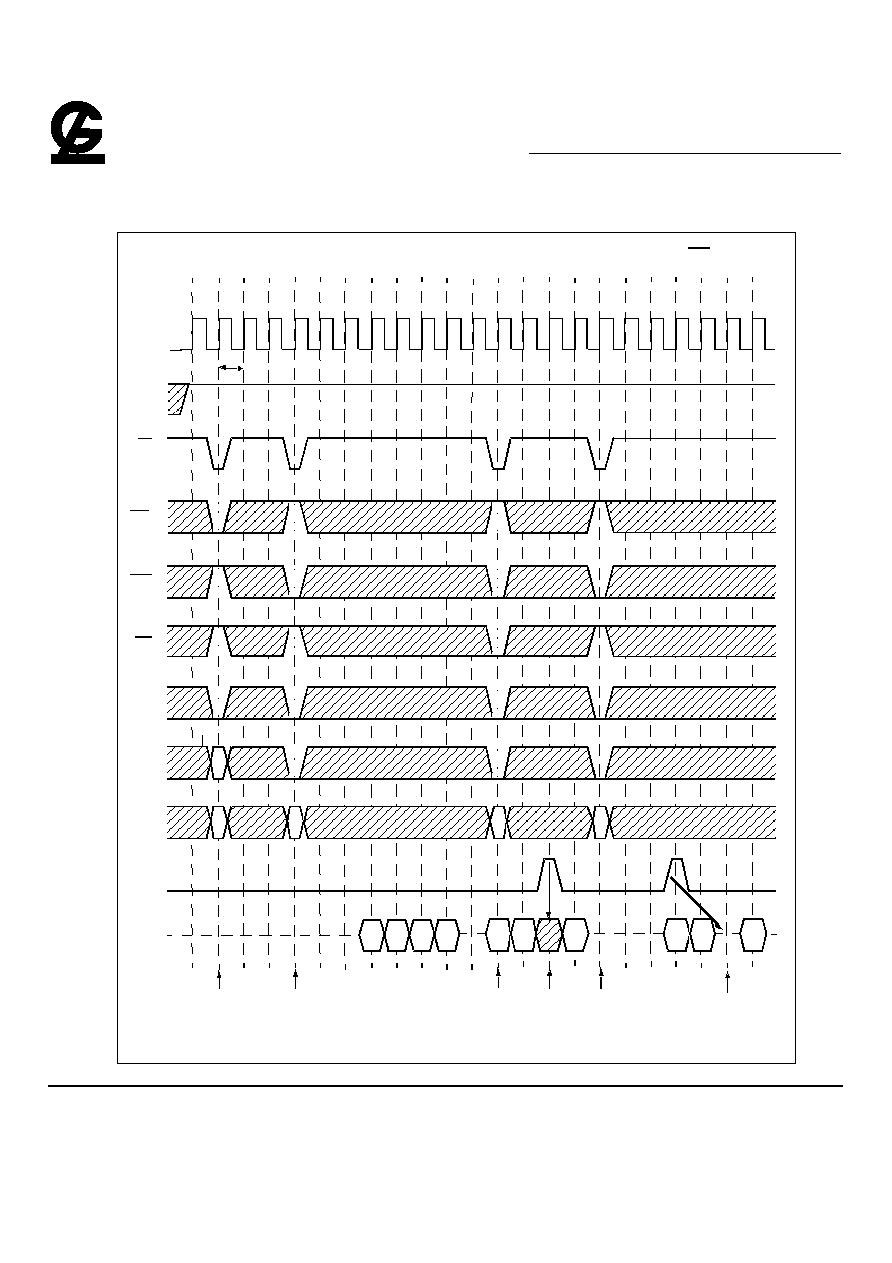
G -LINK
GLT5640AL16
4M X 16 CMOS Synchronous Dynamic RAM
Feb 2004 (Rev.0.1)
G-Link Technology Corporation, Taiwan
Web : www.glink.com.tw Email : sales@glink.com.tw
TEL : 886-2-27968078
- 52 -
Read and Write Cycle (2 of 2)
*BA1="L" , Bank C , D = Idle
T0 T1 T2 T3 T4 T5 T6 T7 T8 T9 T10 T11 T12 T13 T14 T15 T16 T17 T18 T19 T20 T21 T22
CLK
CKE
CS
RAS
CAS
WE
A10
ADD
DQM
DQ
t
CK3
Burst Length=4, CAS Latency=3
Activate
Bank A
Command
Read
Hi-Z
Command
DAb3
QAc0
QAa0 QAa1 QAa2QAa3
DAb0 DAb1
Bank A
Write
Command
Bank A
QAc3
QAc1
The Read Data
The Write
is Masked with a
Zero
RAa
Latency
is Masked with
Two Clock
Latency
RAa
CAb
CAa
CAc
Read
Command
Bank A
*BA0
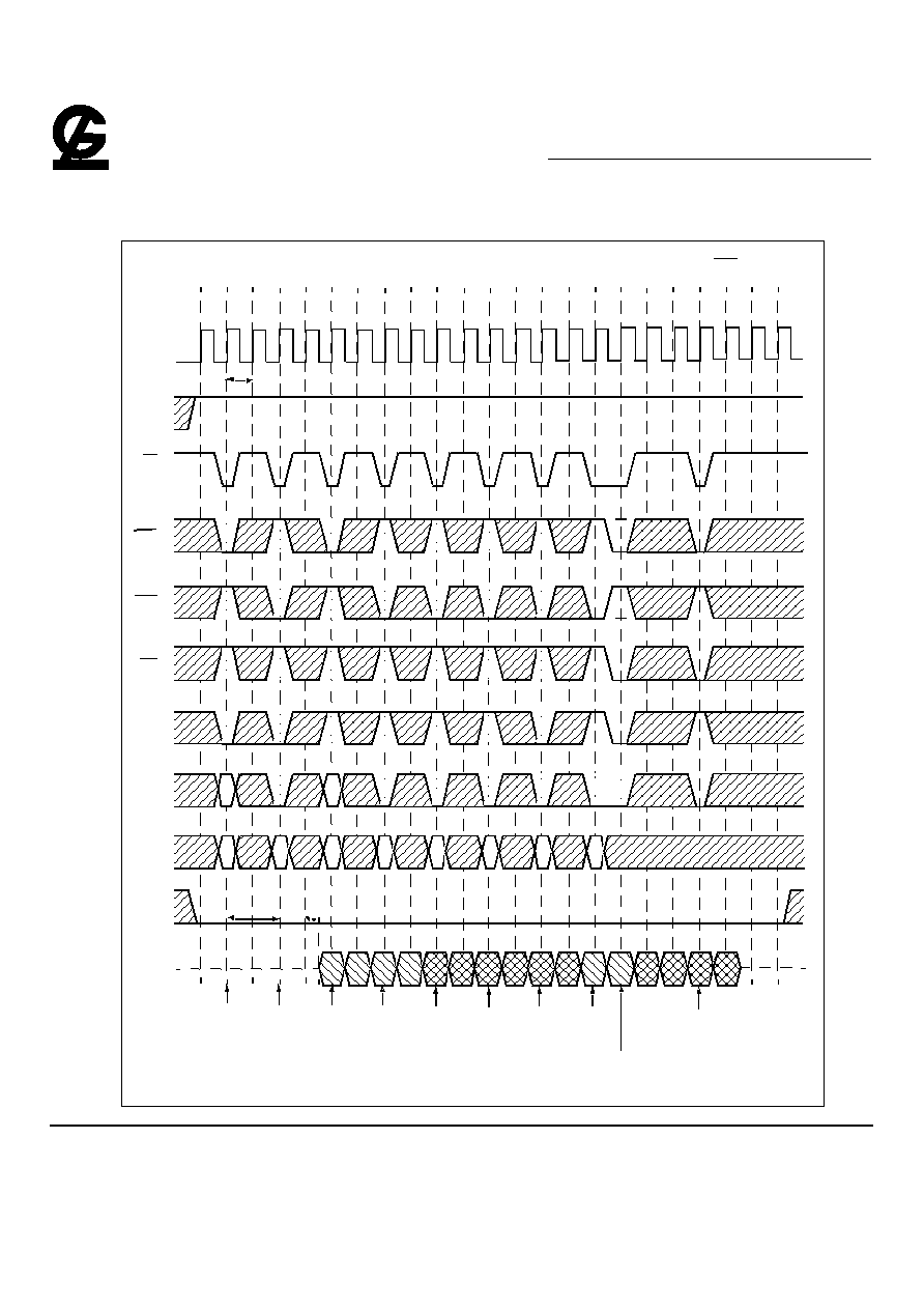
G -LINK
GLT5640AL16
4M X 16 CMOS Synchronous Dynamic RAM
Feb 2004 (Rev.0.1)
G-Link Technology Corporation, Taiwan
Web : www.glink.com.tw Email : sales@glink.com.tw
TEL : 886-2-27968078
- 53 -
Interleaved Column Read Cycle (1 of 2)
*BA1="L" , Bank C , D = Idle
T0 T1 T2 T3 T4 T5 T6 T7 T8 T9 T10 T11 T12 T13 T14 T15 T16 T17 T18 T19 T20 T21 T22
CLK
CKE
CS
RAS
CAS
WE
A10
ADD
DQM
DQ
t
CK2
Burst Length=4, CAS Latency=2
Activate
Bank A
Command
Read
Hi-Z
Command
QBb1
QBd0
QAa0 QAa1 QAa2QAa3 QBa0 QBa1
Bank A
Read
Command
Bank B
QBd2
QBd1
Precharge
Ra
Ra
Ra
Cb
Ra
Ca
Cb
Cc
Cb
Cd
QAb1
QBc0 QBc1
QBd3
Activate
Command
Bank B
Read
Command
Bank B
QBb0
QAb0
Read
Command
Bank B
Read
Command
Bank A
Read
Command
Bank B
Precharge
Command
Bank A
Command
Bank B
t
RCD
t
AC2
*BA0
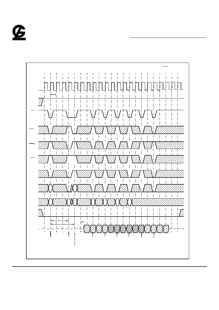
G -LINK
GLT5640AL16
4M X 16 CMOS Synchronous Dynamic RAM
Feb 2004 (Rev.0.1)
G-Link Technology Corporation, Taiwan
Web : www.glink.com.tw Email : sales@glink.com.tw
TEL : 886-2-27968078
- 54 -
Interleaved Column Read Cycle (2 of 2)
*BA1="L" , Bank C , D = Idle
T0 T1 T2 T3 T4 T5 T6 T7 T8 T9 T10 T11 T12 T13 T14 T15 T16 T17 T18 T19 T20 T21 T22
CLK
CKE
CS
RAS
CAS
WE
A10
ADD
DQM
DQ
t
CK3
Burst Length=4, CAS Latency=3
Activate
Bank A
Command
Hi-Z
QBb1
QAb2
QAa0 QAa1 QAa2 QAa3 QBa0 QBa1
QAb3
Precharge
Ra
Ra
Ra
Ca
Ra
Ca
Cb
Cc
Cb
QAb1
QBc0 QBc1
Read
Command
Bank A
Read
Command
Bank B
QBb0
QAb0
Read
Command
Bank B
Read
Command
Bank B
Read
Command
Bank A
Precharge
Command
Bank B
Command
Bank A
t
RRD
Activate
Command
Bank B
t
RCD
t
AC3
*BA0
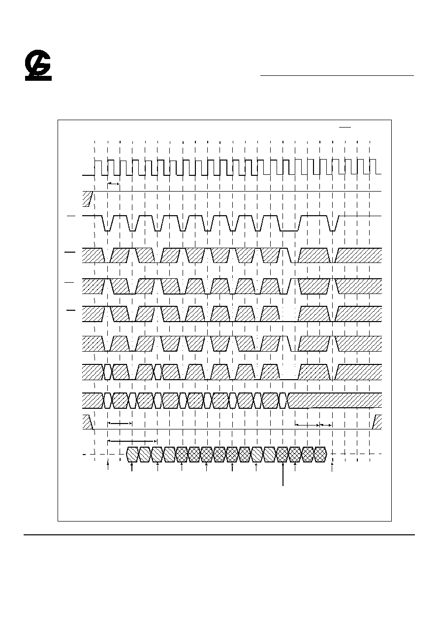
G -LINK
GLT5640AL16
4M X 16 CMOS Synchronous Dynamic RAM
Feb 2004 (Rev.0.1)
G-Link Technology Corporation, Taiwan
Web : www.glink.com.tw Email : sales@glink.com.tw
TEL : 886-2-27968078
- 55 -
Interleaved Column Write Cycle (1 of 2)
*BA1="L" , Bank C , D = Idle
T0 T1 T2 T3 T4 T5 T6 T7 T9 T10 T11 T12 T13 T14 T15 T16 T17 T18 T19 T20 T21 T22
CLK
CKE
CS
RAS
CAS
WE
A10
ADD
DQM
DQ
t
CK2
Burst Length=4, CAS Latency=2
Activate
Bank A
Command
Hi-Z
DBb1
DBd0
DAa0 DAa1 DAa2 DAa3 DBa0 DBa1
DBd1
Precharge
Ra
Ra
Ra
Ca
Ra
Ca
Cb
Cc
Cb
DAb1
DBc0
DBc1
Write
Command
Bank A
Write
Command
Bank B
DBb0
DAb0
Command
Write
Command
Bank B
Write
Command
Bank A
Precharge
Command
Bank A
Command
Bank B
t
RRD
Activate
Command
Bank B
t
RCD
t
RP
Cb
DBd2 DBd3
Write
Bank B
t
DPL
Write
Command
Bank B
*BA0
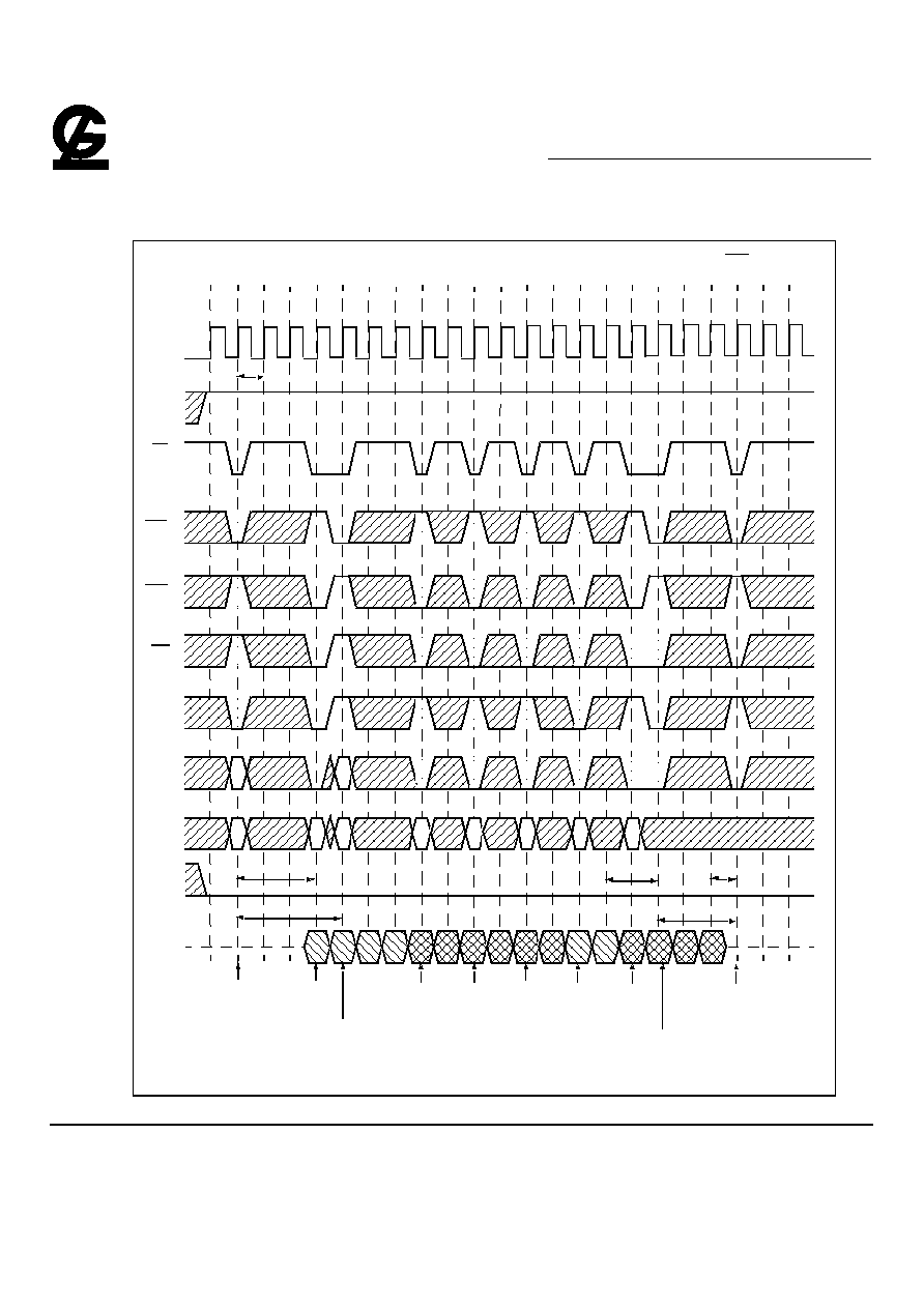
G -LINK
GLT5640AL16
4M X 16 CMOS Synchronous Dynamic RAM
Feb 2004 (Rev.0.1)
G-Link Technology Corporation, Taiwan
Web : www.glink.com.tw Email : sales@glink.com.tw
TEL : 886-2-27968078
- 56 -
Interleaved Column Write Cycle (2 of 2)
*BA1="L" , Bank C , D = Idle
T0 T1 T2 T3 T4 T5 T6 T7 T8 T9 T10 T11 T12 T13 T14 T15 T16 T17 T18 T19 T20 T21 T22
CLK
CKE
CS
RAS
CAS
WE
A10
ADD
DQM
DQ
t
CK3
Burst Length=4, CAS Latency=3
Activate
Bank A
Command
Hi-Z
QBb1
QBd0
QAa0
QAa1 QAa2 QAa3 QBa0
QBa1
QBd1
Precharge
Ra
Ra
Ra
Ca
Ra
Ca
Cb
Cc
Cb
QAb1
QBc0
QBc1
Write
Command
Bank A
Write
Command
Bank B
QBb0
QAb0
Write
Command
Bank B
Write
Command
Bank B
Write
Command
Bank A
Write
Command
Bank B
Command
Bank A
t
RRD
Activate
Command
Bank B
t
RCD
Cd
t
DPL
t
RP
QBd2 QBd3
t
DPL
Precharge
Command
Bank B
*BA0
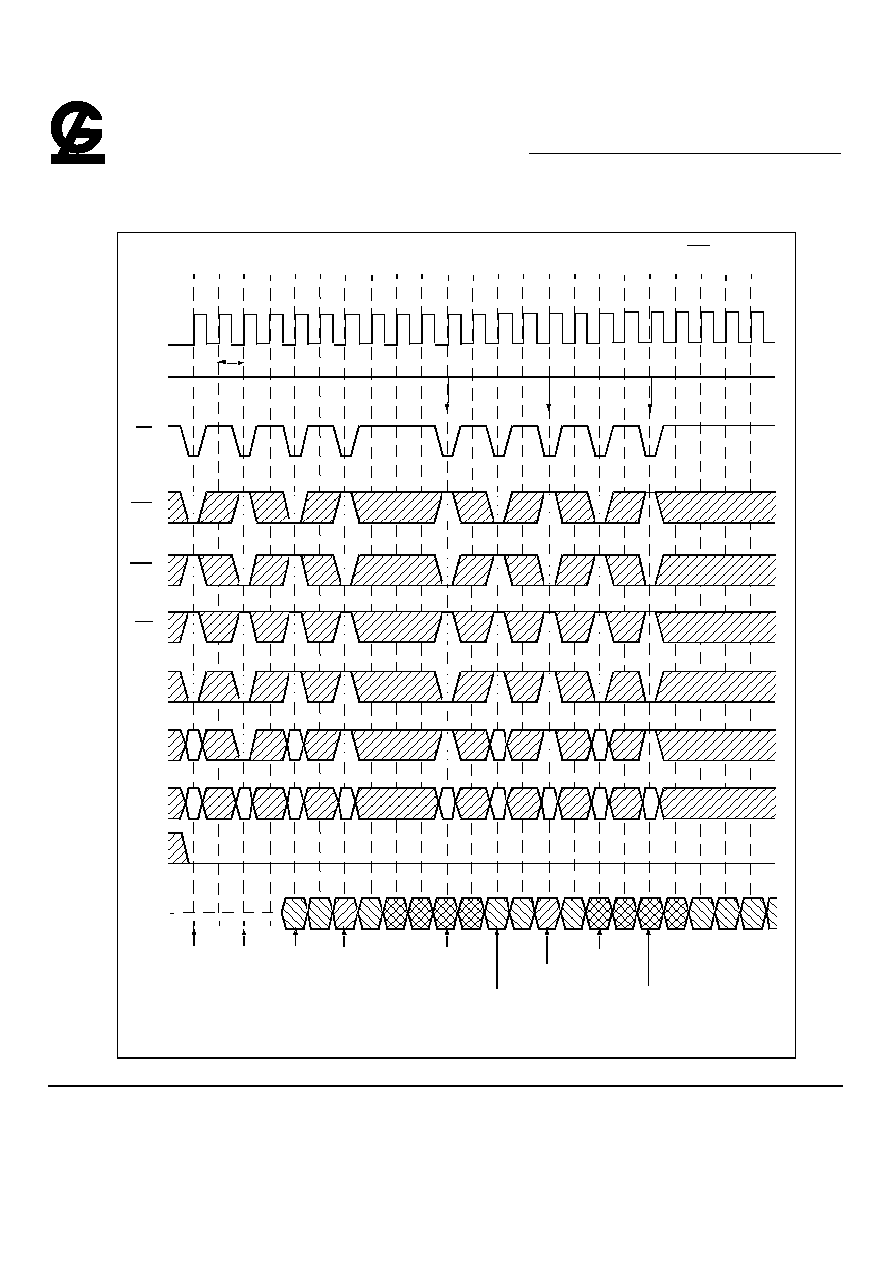
G -LINK
GLT5640AL16
4M X 16 CMOS Synchronous Dynamic RAM
Feb 2004 (Rev.0.1)
G-Link Technology Corporation, Taiwan
Web : www.glink.com.tw Email : sales@glink.com.tw
TEL : 886-2-27968078
- 57 -
Auto Precharge after Read Burst (1 of 2)
*BA1="L" , Bank C , D = Idle
T0 T1 T2 T3 T4 T5 T6 T7 T8 T9 T10 T11 T12 T13 T14 T15 T16 T17 T18 T19 T20 T21 T22
CLK
CKE
CS
RAS
CAS
WE
A10
ADD
DQM
DQ
t
CK2
Burst Length=4, CAS Latency=2
Activate
Bank A
Command
Hi-Z
QBa3
QBb0
QAa0 QAa1 QAa2 QAa3 QBa0
QBa1
QBb1
Read with
Ra
Ra
Ca
Ra
Ca
Cb
Rb
Cb
QAb3
QAb0
QAb1
Activate
Command
Bank B
QBa2
QAb2
Read with
Command
Bank A
Activate
Command
Bank B
Read with
Command
Bank B
Activate
Command
Bank A
Command
Bank A
Read with
Auto Precharge
Bank B
Rc
QBb2 QBb3
Rb
Rc
Ra
Cc
QAc0
QAc2
Read
Bank A
Command
Command
QAc1
Auto Precharge
Auto Precharge
Auto Precharge
Start Auto Precharge
Bank B
Start Auto Precharge
Bank A
Start Auto Precharge
Bank B
High
*BA0
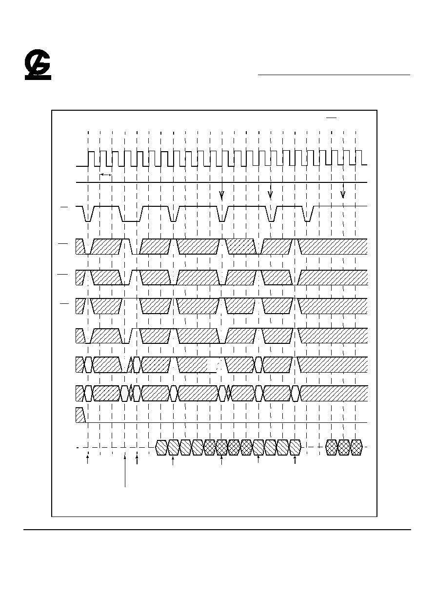
G -LINK
GLT5640AL16
4M X 16 CMOS Synchronous Dynamic RAM
Feb 2004 (Rev.0.1)
G-Link Technology Corporation, Taiwan
Web : www.glink.com.tw Email : sales@glink.com.tw
TEL : 886-2-27968078
- 58 -
Auto Precharge after Read Burst (2 of 2)
*BA1="L" , Bank C , D = Idle
T0 T1 T2 T3 T4 T5 T6 T7 T8 T9 T10 T11 T12 T13 T14 T15 T16 T17 T18 T19 T20 T21 T22
CLK
CKE
CS
RAS
CAS
WE
A10
ADD
DQM
DQ
t
CK3
Burst Length=4, CAS Latency=3
Activate
Bank A
Command
Hi-Z
QBa3
QAa0 QAa1 QAa2 QAa3 QBa0 QBa1
Ra
Ra
Ra
QAb3
QAb0
QAb1
Read
Command
Bank A
Read with
Command
Bank B
QBa2
QAb2
Command
Bank A
Activate
Command
Bank B
QBb0
Ra
Ca
Ca
RBb
Cb
Auto Precharge
Start Auto Precharge
Bank B
Start Auto
Bank A
Start Auto Precharge
Bank B
High
Rb
Cb
QBb1 QBb2
Activate
Command
Bank B
Write with
Auto Precharge
Auto precharge
Command
Bank B
Read with
Rb
Precharge
*BA0
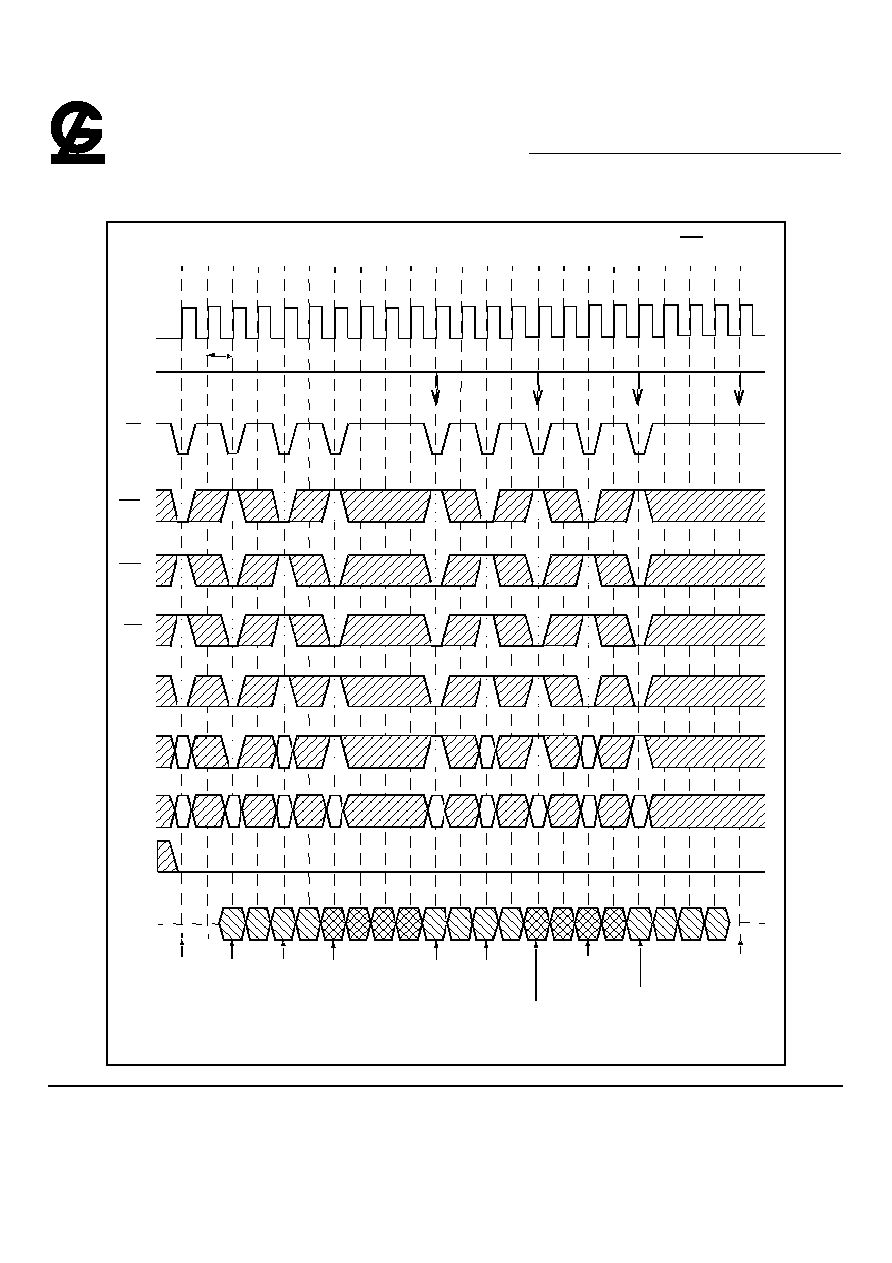
G -LINK
GLT5640AL16
4M X 16 CMOS Synchronous Dynamic RAM
Feb 2004 (Rev.0.1)
G-Link Technology Corporation, Taiwan
Web : www.glink.com.tw Email : sales@glink.com.tw
TEL : 886-2-27968078
- 59 -
Auto Precharge after Write Burst (1 of 2)
*BA1="L" , Bank C , D = Idle
T0 T1 T2 T3 T4 T5 T6 T7 T8 T9 T10 T11 T12 T13 T14 T15 T16 T17 T18 T19 T20 T21 T22
CLK
CKE
CS
RAS
CAS
WE
A10
ADD
DQM
DQ
t
CK2
Burst Length=4, CAS Latency=2
Activate
Bank A
Command
Hi-Z
QBa3
QBb0
QAa0 QAa1 QAa2 QAa3 QBa0 QBa1
QBb1
Ra
Ra
Ra
QAb3
QAb0 QAb1
Write
Command
Bank A
Write with
Command
Bank B
QBa2
QAb2
Write with
Command
Bank A
Activate
Command
Bank B
Write with
Command
Bank B
Activate
Command
Bank B
QBb2 QBb3
Rb
Ra
Ca
Cb
Ca
Rb
Cb
Auto Precharge
Auto Precharge
Auto Precharge
Start Auto
Bank B
Start Auto
Bank A
Start Auto
Bank B
High
Rc
Rc
Cc
QAc0 QAc1 QAc2 QAc3
Activate
Command
Bank A
Write with
Auto Precharge
Bank A
Start Auto
Precharge
Bank A
*BA0
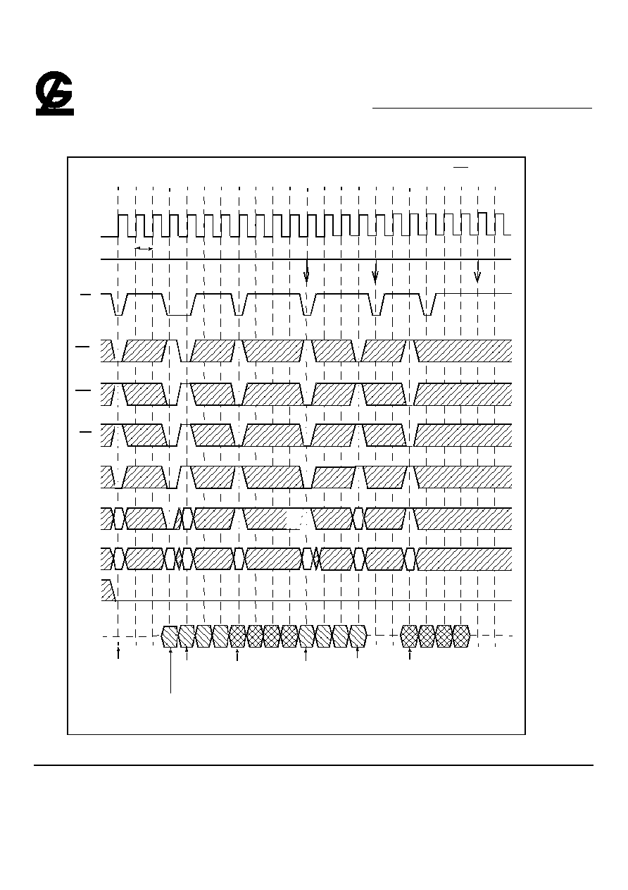
G -LINK
GLT5640AL16
4M X 16 CMOS Synchronous Dynamic RAM
Feb 2004 (Rev.0.1)
G-Link Technology Corporation, Taiwan
Web : www.glink.com.tw Email : sales@glink.com.tw
TEL : 886-2-27968078
- 60 -
Auto Precharge after Write Burst (2 of 2)
T0 T1 T2 T3 T4 T5 T6 T7 T8 T9 T10 T11 T12 T13 T14 T15 T16 T17 T18 T19 T20 T21 T22
CLK
CKE
CS
RAS
CAS
WE
A10
ADD
DQM
DQ
t
CK3
Burst Length=4, CAS Latency=3
Activate
Bank A
Command
Hi-Z
QBa3
QAa0 QAa1 QAa2QAa3 QBa0 QBa1
Ra
Ra
Ra
QAb3
QAb0 QAb1
Read
Command
Bank A
Read with
Command
Bank B
QBa2
QAb2
Command
Bank A
Activate
Command
Bank B
QBb0
Ra
Ca
Ca
RBb
Cb
Auto Precharge
Start Auto Precharge
Bank B
Start Auto
Bank A
Start Auto Precharge
Bank B
High
Rb
Cb
QBb1 QBb2
Activate
Command
Bank B
Write with
Auto Precharge
Auto precharge
Command
Bank B
Read with
Rb
Precharge
QBb3
*BA0

G -LINK
GLT5640AL16
4M X 16 CMOS Synchronous Dynamic RAM
Feb 2004 (Rev.0.1)
G-Link Technology Corporation, Taiwan
Web : www.glink.com.tw Email : sales@glink.com.tw
TEL : 886-2-27968078
- 61 -
*BA1="L" , Bank C , D = Idle
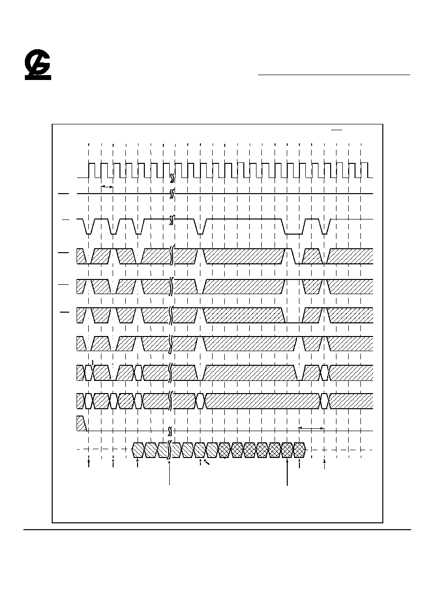
G -LINK
GLT5640AL16
4M X 16 CMOS Synchronous Dynamic RAM
Feb 2004 (Rev.0.1)
G-Link Technology Corporation, Taiwan
Web : www.glink.com.tw Email : sales@glink.com.tw
TEL : 886-2-27968078
- 62 -
Full Page Read Cycle (1 of 2)
*BA1="L" , Bank C , D = Idle
T0 T1 T2 T3 T4 T5 T6 T7 T8 T9 T10 T11 T12 T13 T14 T15 T16 T17 T18 T19 T20 T21 T22
CLK
CKE
CS
RAS
CAS
WE
A10
ADD
DQM
DQ
t
CK2
Burst Length=Full Page, CAS Latency=2
Activate
Bank A
Command
Read
Hi-Z
Command
Ra
QAa+1
Bank A
The burst counter wraps
Burst Stop
Read
Command
Bank B
QAa
Full page burst operation does not
Ra
Ca
Rb
t
RP
High
Activate
Command
Bank B
Ra
Rb
Ca
QAa+2 QAa-2 QAa-1
QAa
QAa+1 QBa
QBa+1 QBa+2 QBa+3 QBa+4 QBa+51QBa+6
Activate
Command
Bank B
from the highest order
page address back to zero
during this time interval
terminate when the burst length is
satisfied; the burst counter
increments and continues bursting
beginning with the starting address
Command
Precharge
Command
Bank B
Ra
*BA0
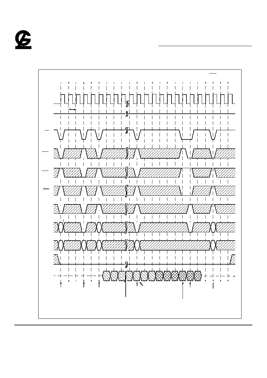
G -LINK
GLT5640AL16
4M X 16 CMOS Synchronous Dynamic RAM
Feb 2004 (Rev.0.1)
G-Link Technology Corporation, Taiwan
Web : www.glink.com.tw Email : sales@glink.com.tw
TEL : 886-2-27968078
- 63 -
Full Page Read Cycle (2 of 2)
*BA1="L" , Bank C , D = Idle
T0 T1 T2 T3 T4 T5 T6 T7 T8 T9 T10 T11 T12 T13 T14 T15 T16 T17 T18 T19 T20 T21 T22
CLK
CKE
CS
RAS
CAS
WE
A10
ADD
DQM
DQ
t
CK3
Burst Length=Full Page, CAS Latency=3
Activate
Bank A
Command
Read
Hi-Z
Ra
QAa+1
Bank A
The burst counter
Burst Stop
Read
Bank B
QAa
Full page burst
Ra
Ca
Rb
High
Activate
Comman
Bank B
Ra
Rb
Ca
QAa+2 QAa-2 QAa-1
QAa QAa+1 QBa0 QBa+1 QBa+2QBa+3 QBa+4 QBa+5
Activate
Bank B
from the highest
page address back to
during this time
Comman
Precharg
Command
Bank B
does not teminate
the burst length is
the burst counter
and continues
beginning with the
addres
Ra
*BA0
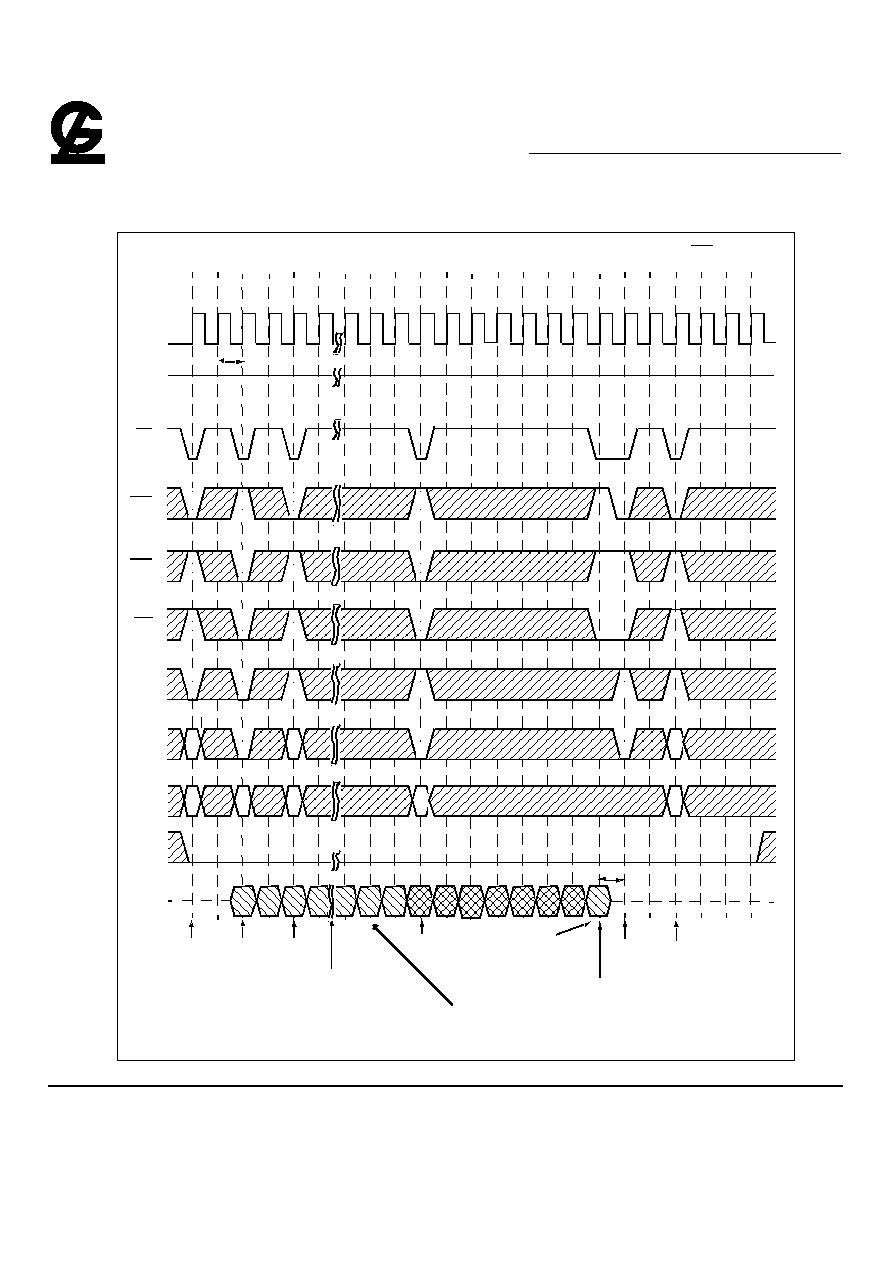
G -LINK
GLT5640AL16
4M X 16 CMOS Synchronous Dynamic RAM
Feb 2004 (Rev.0.1)
G-Link Technology Corporation, Taiwan
Web : www.glink.com.tw Email : sales@glink.com.tw
TEL : 886-2-27968078
- 64 -
Full Page Write Cycle (1 of 2)
*BA1="L" , Bank C , D = Idle
T0 T1 T2 T3 T4 T5 T6 T7 T8 T9 T10 T11 T12 T13 T14 T15 T16 T17 T18 T19 T20 T21 T22
CLK
CKE
CS
RAS
CAS
WE
A10
ADD
DQM
DQ
t
CK2
Burst Length=Full Page, CAS Latency=2
Activate
Bank A
Command
Write
Hi-Z
Command
Ra
QAa+1
Bank A
The burst counter wraps
Burst Stop
Write
Command
Bank B
QAa
Full page burst operation
Ra
Ca
Rb
t
BDL
High
Activate
Command
Bank B
Ra
Rb
Ca
QAa+2
QAa+3
QAa-1
QAa
QAa+1
QBa
QBa+1
QBa+2
QBa+3
QBa+4
QBa+5
Activate
Command
Bank B
from the highest order
page address back to zero
during this time interval
Command
Precharge
Command
Bank B
does not terminate when
the burst length is satisfied;
the burst counter increments
and continues bursting
beginning with the starting
address
QBa+6
Data is ignored
Ra
*BA0
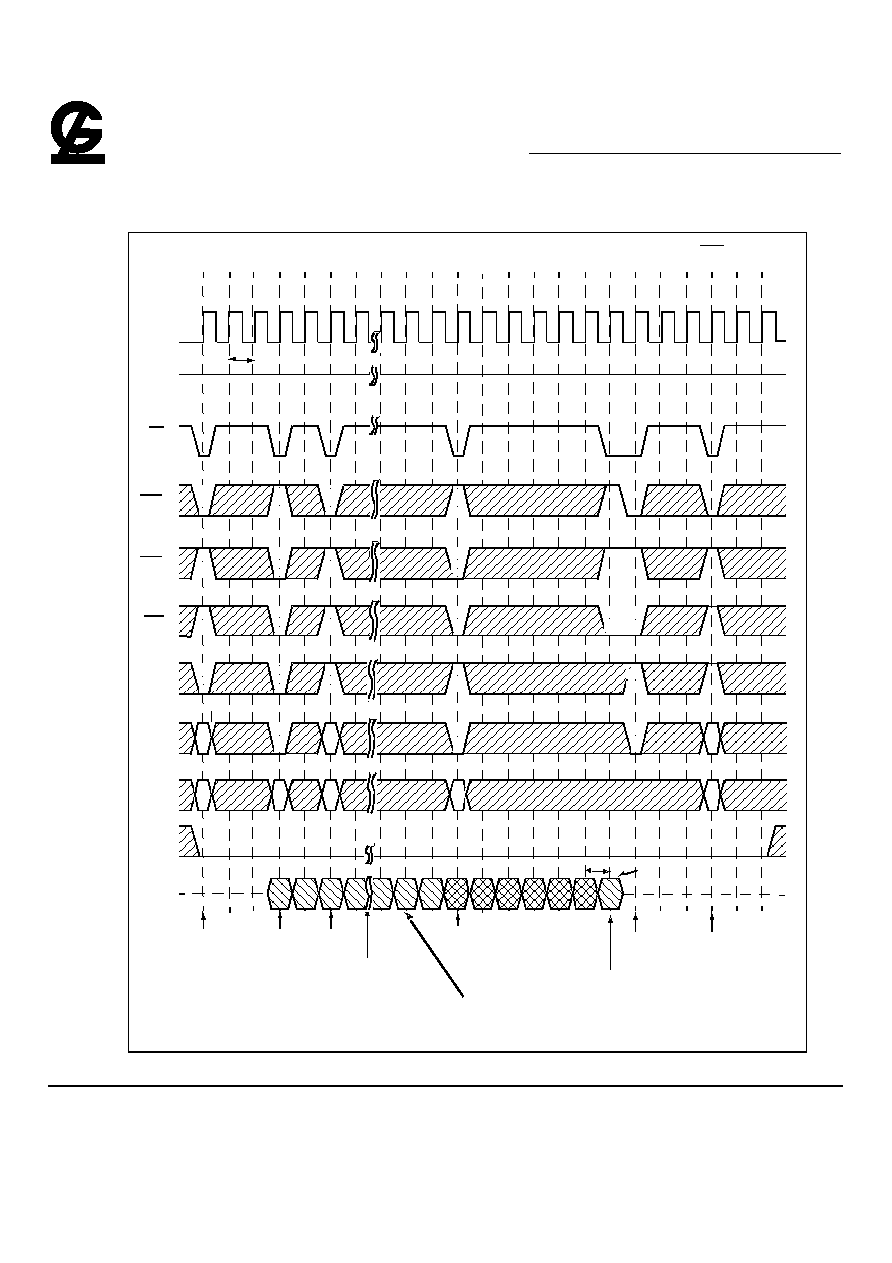
G -LINK
GLT5640AL16
4M X 16 CMOS Synchronous Dynamic RAM
Feb 2004 (Rev.0.1)
G-Link Technology Corporation, Taiwan
Web : www.glink.com.tw Email : sales@glink.com.tw
TEL : 886-2-27968078
- 65 -
Full Page Write Cycle (2 of 2)
*BA1="L" , Bank C , D = Idle
T0 T1 T2 T3 T4 T5 T6 T7 T8 T9 T10 T11 T12 T13 T14 T15 T16 T17 T18 T19 T20 T21 T22
CLK
CKE
CS
RAS
CAS
WE
A10
ADD
DQM
DQ
t
CK3
Burst Length=Full Page, CAS Latency=3
Activate
Bank A
Command
Write
Hi-Z
Command
Ra
DAa+1
Bank A
The burst counter wraps
Burst Stop
Write
Command
Bank B
DAa
Full page burst operation
Ra
t
BDL
High
Activate
Command
Bank B
DAa+2
DAa+3
DAa-1
DAa
DAa+1
DBa
DBa+1
DBa+2
DBa+3
DBa+4
DBa+5
Activate
Command
Bank B
from the highest order
page address back to zero
during this time interval
Command
Precharge
Command
Bank B
does not terminate when
the burst length is satisfied;
the burst counter increments
and continues bursting
beginning with the starting
address
Ra
Rb
Ca
Ra
Ca
Rb
Data is ignored.
*BA0
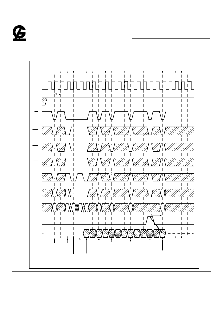
G -LINK
GLT5640AL16
4M X 16 CMOS Synchronous Dynamic RAM
Feb 2004 (Rev.0.1)
G-Link Technology Corporation, Taiwan
Web : www.glink.com.tw Email : sales@glink.com.tw
TEL : 886-2-27968078
- 66 -
Full Page Random Column Read
*BA1="L" , Bank C , D = Idle
T0 T1 T2 T3 T4 T5 T6 T7 T8 T9 T10 T11 T12 T13 T14 T15 T16 T17 T18 T19 T20 T21 T22
CLK
CKE
CS
RAS
CAS
WE
BA
A10
ADD
DQM
DQ
t
CK2
Burst Length=Full Page, CAS Latency=2
Activate
Bank A
Command
Activate
Hi-Z
Ra
QBa0
Bank B
Read
Bank B
QAa0
Ra
Activate
Comman
Bank B
QAb0 QAb1
QBb0 QBb1 QAc0 QAc1
QAc2 QBc0 QBc1
QBc2
Read
Bank A
Precharg
Cc
Cc
Rb
Ra
Ra
Ca
Ca
Cb
Cb
Rb
t
RP
Read
Bank B
Read
Bank A
Read
Bank A
Read
Bank B
Command Bank
(Precharge
(Bank D)
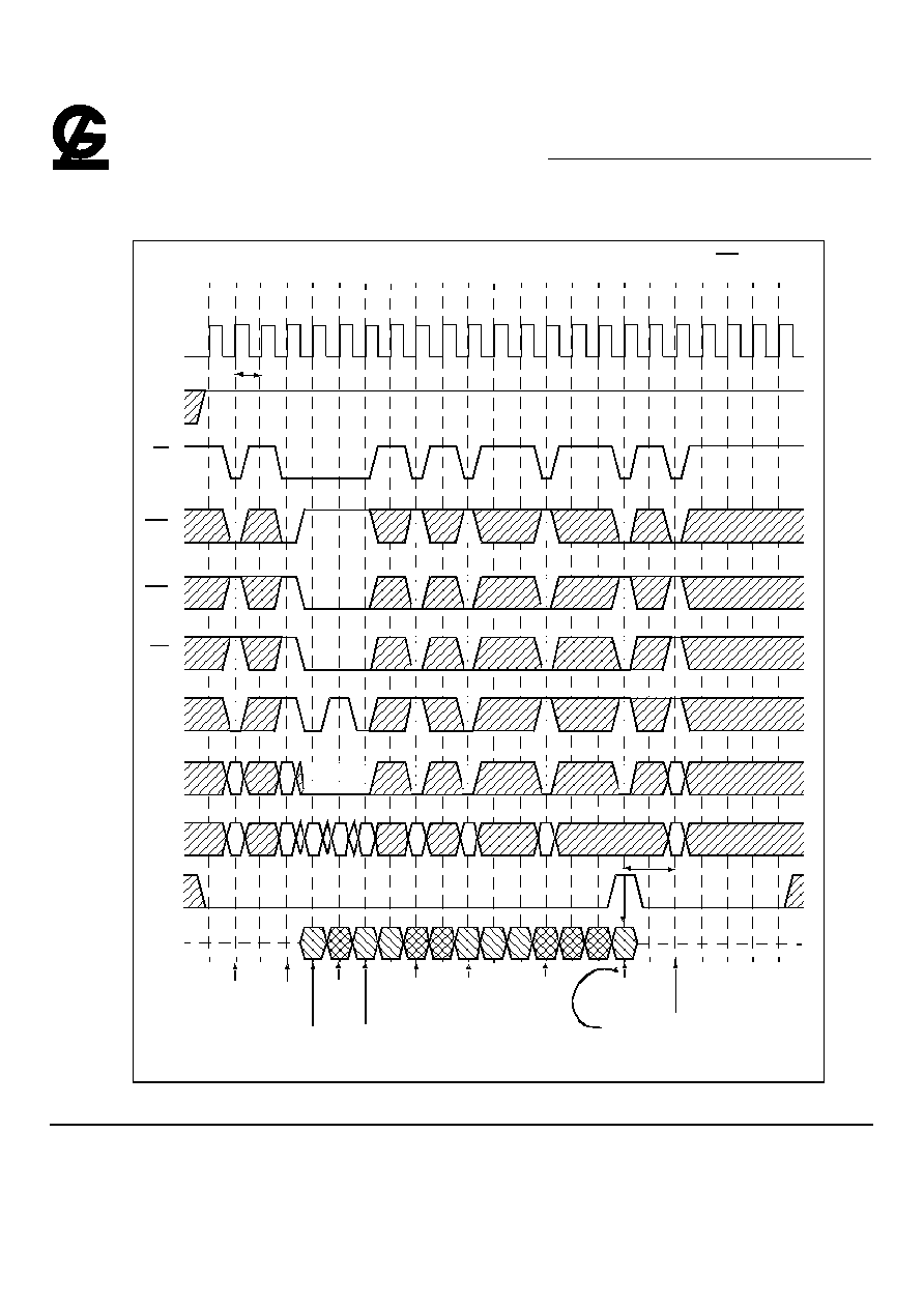
G -LINK
GLT5640AL16
4M X 16 CMOS Synchronous Dynamic RAM
Feb 2004 (Rev.0.1)
G-Link Technology Corporation, Taiwan
Web : www.glink.com.tw Email : sales@glink.com.tw
TEL : 886-2-27968078
- 67 -
Full Page Random Column Write
*BA1="L" , Bank C , D = Idle
T0 T1 T2 T3 T4 T5 T6 T7 T8 T9 T10 T11 T12 T13 T14 T15 T16 T17 T18 T19 T20 T21 T22
CLK
CKE
CS
RAS
CAS
WE
A10
ADD
DQM
DQ
t
CK2
Burst Length=Full Page, CAS Latency=2
Activate
Bank A
Command
Activate
Hi-Z
Command
Ra
QBa0
Bank B
Write
Command
Bank B
QAa0
Ra
Activate
Command
Bank B
QAb0 QAb1 QBb0 QBb1 QAc0
QAc1 QAc2
QBc0 QBc1 QBc2
Write
Command
Bank A
Precharge
Cc
Cc
Rb
Ra
Ra
Ca
Ca
Cb
Cb
Rb
t
RP
Write
Command
Bank B
Write
Command
Bank A
Write
Command
Bank A
Write
Command
Bank B
Command Bank B
(Precharge Termination)
Write Data
is masked
(Bank D)
*BA0
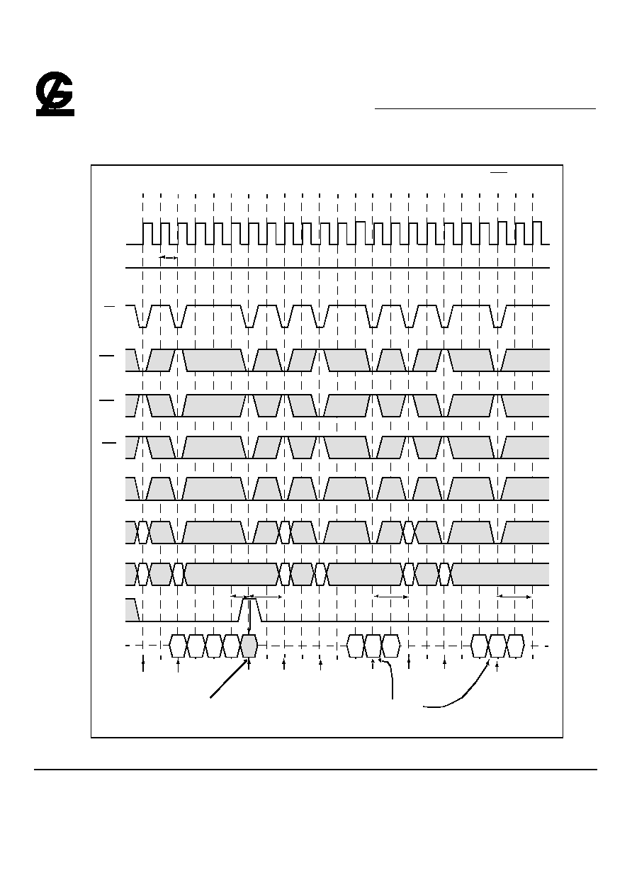
G -LINK
GLT5640AL16
4M X 16 CMOS Synchronous Dynamic RAM
Feb 2004 (Rev.0.1)
G-Link Technology Corporation, Taiwan
Web : www.glink.com.tw Email : sales@glink.com.tw
TEL : 886-2-27968078
- 68 -
Precharge Termination of a Burst (1 of 2)
*BA1="L" , Bank C , D = Idle
T0 T1 T2 T3 T4 T5 T6 T7 T8 T9 T10 T11 T12 T13 T14 T15 T16 T17 T18 T19 T20 T21 T22
CLK
CKE
CS
RAS
CAS
WE
A10
ADD
DQM
DQ
t
CK2
Burst Length=8, CAS Latency=2
Activate
Bank A
Command
Write
Hi-Z
Command
RAa
Bank A
Activate
Command
Bank A
Read
Command
Bank A
RAc
CAb
RAb
RAb
RAc
Precharge Termination
o f a Write Burst. Write
da ta is masked.
Precharge
Command
Read
Command
Bank A
Precharge
Command
Bank A
Precharge Termination
High
RA a
C A c
CAa
QAa1
QAa0
QAa2
Da3
QAb0
QAb1
QAb2
QAc0
QAc1
QAc2
t
DPL
t
RP
t
RP
t
RP
Bank A
o f a Read Burst.
Activate
Command
Bank A
Precharge
Command
Bank A
*BA0
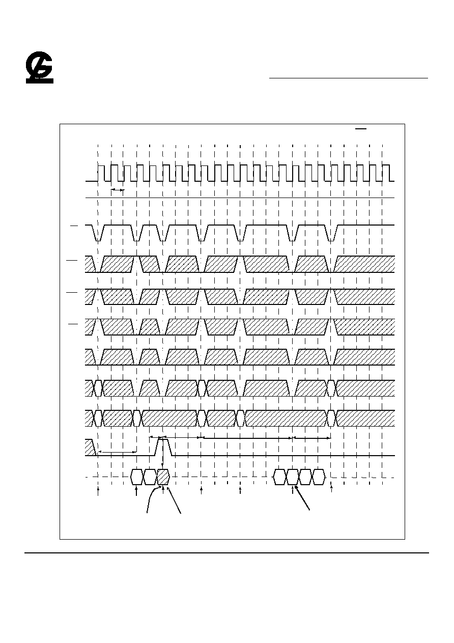
G -LINK
GLT5640AL16
4M X 16 CMOS Synchronous Dynamic RAM
Feb 2004 (Rev.0.1)
G-Link Technology Corporation, Taiwan
Web : www.glink.com.tw Email : sales@glink.com.tw
TEL : 886-2-27968078
- 69 -
Precharge Termination of a Burst (2 of 2)
*BA1="L" , Bank C , D = Idle
T0 T1 T2 T3 T4 T5 T6 T7 T8 T9 T10 T11 T12 T13 T14 T15 T16 T17 T18 T19 T20 T21 T22
CLK
CKE
CS
RAS
CAS
WE
A10
ADD
DQM
DQ
t
CK3
Activate
Bank A
Command
Write
Hi-Z
Command
RAa
Bank A
Activate
Command
Bank A
CAb
RAb
RAb
RAc
Precharge
Command
Read
Command
Bank A
High
RAa
RAc
CAa
DAa1
DAa0
QAb0 QAb1
QAb2 QAb3
t
DPL
t
RP
Bank A
Activate
Command
Bank A
Activate
Command
Bank A
t
RCD
t
RP
Write Data
is masked
Precharge Termination
of a Write Burst.
Precharge Termination
of a Read Burst.
t
RAS
*BA0
Burst Length=8, CAS Latency=3
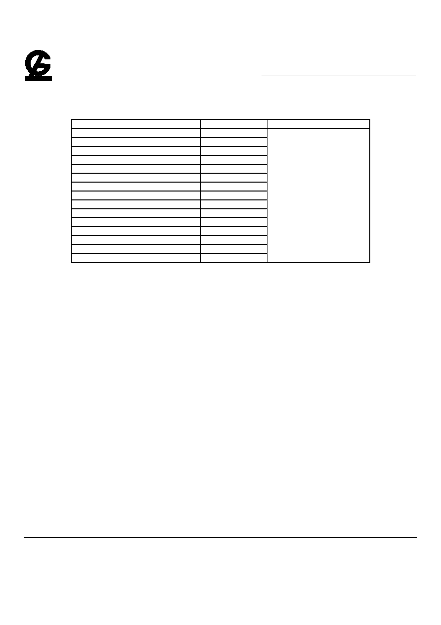
G -LINK
GLT5640AL16
4M X 16 CMOS Synchronous Dynamic RAM
Feb 2004 (Rev.0.1)
G-Link Technology Corporation, Taiwan
Web : www.glink.com.tw Email : sales@glink.com.tw
TEL : 886-2-27968078
- 70 -
Ordering information
Part Number
Cycle time
Package
GLT5640AL16 - 5.5TC
5.5 ns
GLT5640AL16 - 6TC
6 ns
GLT5640AL16 - 7TC
7 ns
GLT5640AL16 - 8TC
8 ns
GLT5640AL16 - 10TC
10 ns
GLT5640AL16P - 5.5TC
5.5 ns
GLT5640AL16P - 6TC
6 ns
GLT5640AL16P - 7TC
7 ns
GLT5640AL16P - 8TC
8 ns
GLT5640AL16P - 10TC
10 ns
GLT5640AL16L - 5.5TC
5.5 ns
GLT5640AL16L - 6TC
6 ns
GLT5640AL16L - 7TC
7 ns
GLT5640AL16L - 8TC
8 ns
GLT5640AL16L - 10TC
10 ns
400mil, 54-Pin
Plastic TSOP
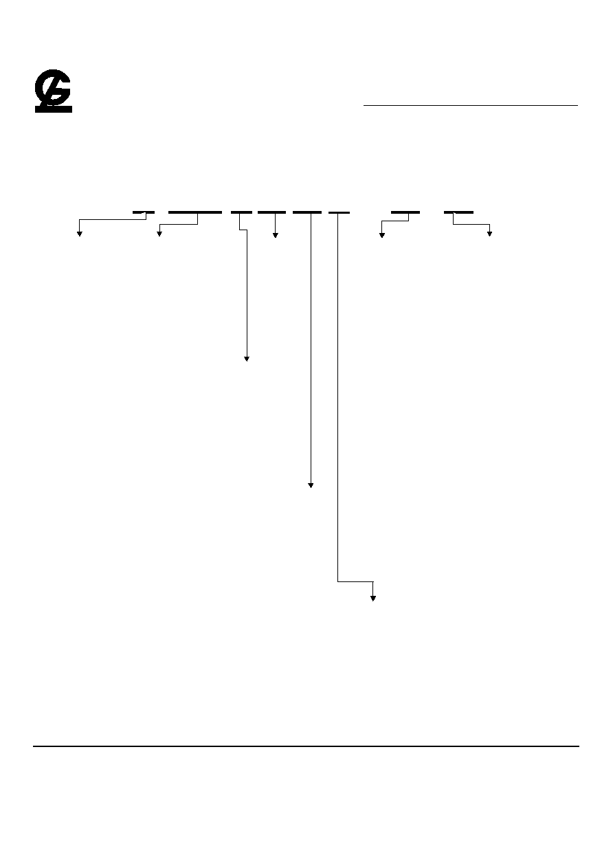
G -LINK
GLT5640AL16
4M X 16 CMOS Synchronous Dynamic RAM
Feb 2004 (Rev.0.1)
G-Link Technology Corporation, Taiwan
Web : www.glink.com.tw Email : sales@glink.com.tw
TEL : 886-2-27968078
- 71 -
Parts Numbers (Top Mark) Definition :
GLT 5 640A L 16 P - 7 TC
4 : DRAM
5 : Synchronous
DRAM
6 : Standard SRAM
/Pseudo SRAM
7 : Cache SRAM
8 : Synchronous
Burst SRAM
9 : SGRAM
-SRAM
064 : 64K
256 : 256K
512 : 512K
100 : 1M
200 : 2M
400 : 4M
-DRAM
10 : 1M(C/EDO)
11 : 1M(C/FPM)
12 : 1M(H/EDO)
13 : 1M(H/FPM)
20 : 2M(EDO)
21 : 2M(FPM)
40 : 4M(EDO)
41 : 4M(FPM)
80 : 8M(EDO)
81 : 8M(FPM)
160 : 16M(EDO)
161 : 16M(FPM)
640 : 64M(EDO)
641 : 64M(FPM)
-SDRAM
40 : 4M
160 : 16M
320 : 32M,4Bank
640 : 64M
640A : 64M
1280 : 128M
-PSEUDO SDRAM
020 2M
160 16M
320 32M
VOLTAGE
Blank : 5V
L : 3.3V
M : 2.5V
N : 2.0V
CONFIG.
04 : x04
08 : x08
16 : x16
32 : x32
SPEED
-SRAM/PSEUDO SRAM
12 : 12ns
15 : 15ns
20 : 20ns
55 : 55ns
70 : 70ns
85 : 85ns
120 : 120ns
-DRAM
25 : 25ns
28 : 28ns
30 : 30ns
35 : 35ns
40 : 40ns
45 : 45ns
50 : 50ns
60 : 60ns
70 : 70ns
80 : 80ns
100 : 100ns
SDRAM
5 : 5ns/200 MHZ
5.5 : 5.5ns/183 MHZ
6 : 6ns/166 MHZ
7 : 7ns/143 MHZ
8 : 8ns/125 MHZ
10 : 10ns/100 MHZ
PACKAGE
T : PDIP(300mil)
TS : TSOP(Type I)
ST : sTSOP(Type I)
TC : TSOPll (40/44)
PL : PLCC
FA : 300mil SOP
FB : 330mil SOP
FC : 445mil SOP
J3 : 300mil SOJ
J4 : 400mil SOJ
P : PDIP(600mil)
Q : PQFP
TQ : TQFP
FG : 48Pin BGA 9x12
FH : 48Pin BGA 8x10
FI : 48Pin BGA 6x8
FJ : 60Ball VFBGA
POWER
Blank : Standard
L : Low Power
LL : Low Low Power
SL : Super Low Power
Temperature Range
E : Extended Temperature
I : Industrial Temperature
Blank : Commercial Temperature
P : Pb free part
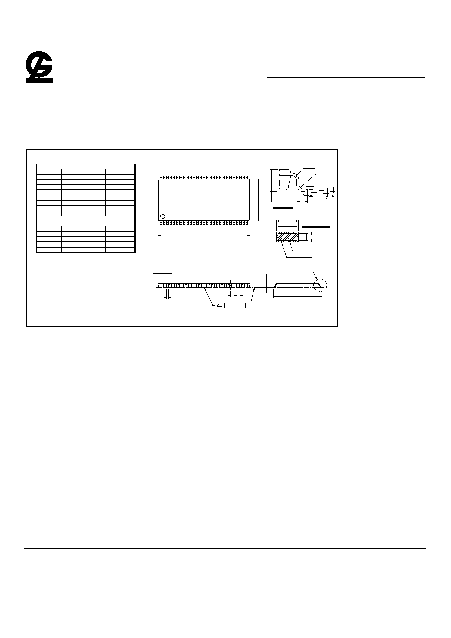
G -LINK
GLT5640AL16
4M X 16 CMOS Synchronous Dynamic RAM
Feb 2004 (Rev.0.1)
G-Link Technology Corporation, Taiwan
Web : www.glink.com.tw Email : sales@glink.com.tw
TEL : 886-2-27968078
- 72 -
Packaging Information
·
400mil, 54-Pin Plastic TSOP
1. CONTROLLING DIMENSION : MILLIMETERS
2. DIMENSION D DOES NOT INCLUDE MOLD PROTRUSION.
MOLD PROTRUSION SHALL NOT EXCEED 0.15mm(0.006") PER SIDE.
DIMENSION E1 DOES NOT INCLUDE INTERLEAD PROTRUSION.
INTERLEAD PROTRUSION SHALL NOT EXCEED 0.25mm(0.01") PER SIDE.
3. DIMENSION b DOES NOT INCLUDE DAMBAR PROTRUSIONS/INTRUSION.
ALLOWABLE DAMBAR PROTRUSION SHALL NOT CAUSE THE LEAD TO
DAMBAR INTRUSION SHALL NOT CAUSE THE LEAD TO BE NARROWER
THAN THE MIN b DIMENSION BY MORE THAN 0.07mm.
BE WIDER THAN THE MAX b DIMENSION BY MORE THAN 0.13mm.
NOTE:
22.09
11.56
10.03
R1
ZD
E1
L
R
E
e
c
D
c1
b1
b
A
A1
A2
DIM
---
---
---
---
0.12
0.005
0.012
0.012
0.005
0.005
0.870
0.455
0.016
0.005
0.395
0.71 REF.
0.80 BASIC
10.16
0.40
0.12
0.50
---
11.76
10.29
0.25
0.60
11.96
---
0.12
0.12
22.22
---
0.30
0.30
---
---
0.21
22.35
0.16
0.45
0.40
0.028 REF.
0.400
0.020
---
0.463
0.0315 BASIC
0.405
0.024
0.010
0.471
---
0.875
---
---
---
0.008
0.880
0.006
0.016
0.018
MIN.
0.002
0.037
MILLIMETERS
---
---
0.05
0.95
---
1.00
MIN.
NOM.
1.20
0.15
1.05
MAX.
---
---
0.039
---
INCHES
NOM.
0.047
0.006
0.041
MAX.
A
b
0.100(0.004")
e
E
SEATING PLANE
28
27
D
ZD
1
54
c
B
RAD R
A2
A1
E1
DETAIL A
DETAIL A
B
L
0¢X~8¢X
RAD R1
c1
c
BASE METAL
WITH PLATING
SECTION B-B
b1
b