 | –≠–ª–µ–∫—Ç—Ä–æ–Ω–Ω—ã–π –∫–æ–º–ø–æ–Ω–µ–Ω—Ç: GS2911N15 | –°–∫–∞—á–∞—Ç—å:  PDF PDF  ZIP ZIP |
www.globaltechsemi.com 1 GS2911
GS2911
300mA CMOS Positive LDO Voltage Regulator
Product Description
The GS2911 is a positive voltage output, three-pin regulator that provides a high current even
when the input/output voltage differential is small. Low power consumption and high accuracy
is achieved through CMOS and laser trimming technologies.
The GS2911 consists of a high-precision voltage reference, an error correction circuit, and a
current limited output driver. Transient response to load variations has improved in comparison
to the existing series.
TO-92 and SOT-89 packages are available.
Features
Applications
Maximum output current: 250mA (within
the maximum power dissipation,
V
OUT
=5.0V)
Output voltage: 2.0V to 6.0V in 0.1V
increments (1.1V to 1.9V for custom
products)
Highly accurate: Output voltage ± 2%
(±1% for semi-custom products)
Low power consumption: Typ. 2.0µA at
V
OUT
= 5.0V
Output voltage temperature coefficient
0.1%/V: Typ. ± 100ppm/
Input stability: Typ. 2.0%/V
Small input/output differential: I
OUT
=
100mA at V
OUT
= 5.0V with a 0.12V
differential.
SOT-89 and TO-92 packages are
available
Wireless Communication Systems
Battery Powered Systems
Palmtops
Portable Cameras and Video Recorders
Voltage Regulator for Microprocessor
Voltage Regulator for CD-ROM Drivers,
LAN Cards, 56K Modem
GS2911 Globaltech Semiconductor
www.globaltechsemi.com 2 GS2911
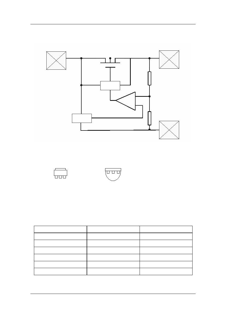
Block Diagram
Vout
Vin
Vss
Current
Limiter
+
-
Voltage
Reference
Package and Pin Assignments
GS2911YXX (SOT-89)
GS2911NXX (TO-92)
1
2
3
Pin1 = GND
Pin2 = V
IN
Pin3 = V
OUT
1 2 3
Pin1 = GND
Pin2 = V
IN
Pin3 = V
OUT
Ordering Information
SOT-89 TO-92 Output
GS2911Y15 GS2911N15
1.5V
GS2911Y18 GS2911N18
1.8V
GS2911Y20 GS2911N20
2.0V
GS2911Y25 GS2911N25
2.5V
GS2911Y33 GS2911N33
3.3V
GS2911Y50 GS2911N50
5.0V
*For additional available fixed voltages contact factory.
*Add "F" means lead free part.
GS2911 Globaltech Semiconductor
www.globaltechsemi.com 3 GS2911
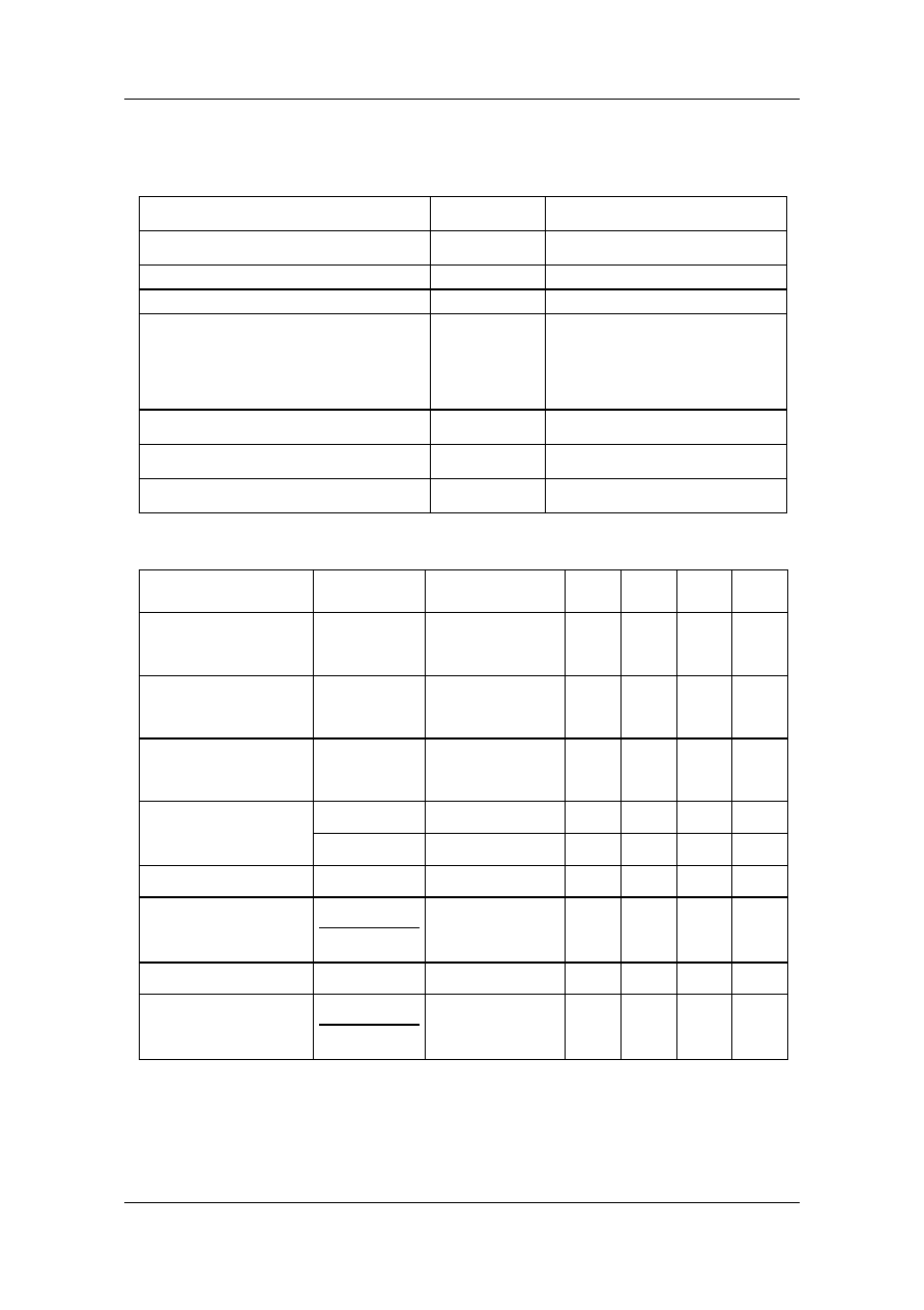
Absolute Maximum Ratings
Parameter Symbol
Ratings
Input Voltage
V
IN
12V
Output Current
I
OUT
500
mA
Output Voltage
V
OUT
Vss-0.3 to V
IN+
0.3
Continuous Total Power Dissipation
TO-92
SOT-89
P
D
500 mW
550 mW
Operating Ambient Temperature
T
opr
0 to 80
Storage temperature Range
T
stg
-40 to 125
Lead Temperature (10 sec)
T
LEAD
260
Electrical Characteristics
V
OUT
(T) =2.0 (Note 1)
Parameter Symbol
Conditions
Min
Typ.
Max
Unit
Output voltages
V
OUT
(E)
(Note 2)
I
OUT
= 40mA
V
IN
= 3.0V
1.960
2.000 2.040 V
Maximum output current
I
OUT
max
V
IN
= 3.0V
V
OUT
(E) 1.8V
100
mA
Load stability
V
OUT
V
IN
= 3.0V
1mA I
OUT
60mA
45 90
mV
Vdif I
OUT
=60mA
180
360
mV
Input-Output
Voltage differential (Note 3)
I
OUT
=120mA
400
700
mV
Supply current
I
SS
V
IN
= 3.0V
1.0
100
µA
Line regulation
V
OUT
V
IN
* V
OUT
I
OUT
= 40mA
3.0VV
IN
10.0V
0.2
0.3
%/V
Input voltage
V
IN
10
V
Output voltage
Temperature characteristics
V
OUT
Topr * V
OUT
I
OUT
= 40mA
-40Topr85
±
100 ppm/
GS2911 Globaltech Semiconductor
www.globaltechsemi.com 4 GS2911
Electrical Characteristics
V
OUT
(T) =2.5V (Note 1)
Parameter Symbol
Conditions
Min
Typ.
Max
Unit
Output voltages
V
OUT
(E)
(Note 2)
I
OUT
= 40mA
V
IN
= 3.5V
2.450
2.500 2.550 V
Maximum output current
I
OUT
max
V
IN
= 3.5V
V
OUT
(E) 2.25V
150
mA
Load stability
V
OUT
V
IN
= 3.5V
1mA I
OUT
80mA
45 90
mV
Vdif I
OUT
=80mA
180
360
mV
Input-Output
Voltage differential (Note 3)
I
OUT
=160mA
400
700
mV
Supply current
Iss
V
IN
= 3.5V
1.0
100
µA
Line regulation
V
OUT
V
IN
* V
OUT
I
OUT
= 40mA
3.5VV
IN
10.0V
0.2
0.3
%/V
Input voltage
V
IN
10
V
Output voltage
Temperature characteristics
V
OUT
Topr * V
OUT
I
OUT
= 40mA
-40Topr85
±
100 ppm/
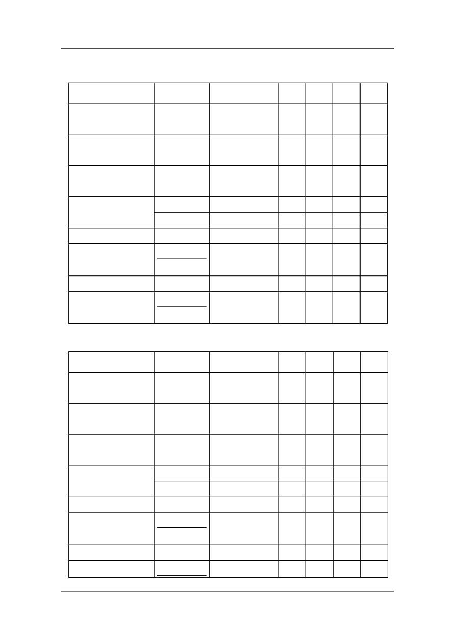
Electrical Characteristics
V
OUT
(T) =3.3 (Note 1)
Parameter Symbol
Conditions
Min
Typ.
Max
Unit
Output voltages
V
OUT
(E)
(Note 2)
I
OUT
= 40mA
V
IN
= 4.3V
3.234
3.3 3.366 V
Maximum output current
I
OUT
max
V
IN
= 4.3V
V
OUT
(E) 2.97V
165
mA
Load stability
V
OUT
V
IN
= 4.3V
1mA I
OUT
80mA
45 90
mV
Vdif
VIN = 4.3V
Input-Output
Voltage differential (Note 3)
IOUT=160mA
400
700
mV
Supply current
Iss
V
IN
= 4.3V
1.0
100
µA
Line regulation
V
OUT
V
IN
* V
OUT
I
OUT
= 40mA
4.3VV
IN
10.0V
0.2
0.3
%/V
Input voltage
V
IN
10
V
Output voltage
V
OUT
I
OUT
= 40mA
±
100 ppm/

GS2911 Globaltech Semiconductor
www.globaltechsemi.com 5 GS2911
Temperature characteristics
Topr * V
OUT
-40Topr125
Electrical Characteristics
V
OUT
(T) =5.0 (Note 1)
Parameter Symbol
Conditions
Min
Typ
Max
Unit
Output voltages
V
OUT
(E)
(Note 2)
I
OUT
= 40mA
V
IN
= 6.0V
4.900
5.000 5.100 V
Maximum output current
I
OUT
max
V
IN
= 6.0V
V
OUT
(E)
5.0V
165
mA
Load stability
V
OUT
V
IN
= 6.0V
1mA
I
OUT
80mA
45 90
mV
Vdif V
IN
= 6.0V
Input-Output
Voltage differential (Note 3)
Vdif I
OUT
=200mA
380
600
mV
Supply current
Iss
V
IN
= 6.0V
1.0
100
µA
Line regulation
V
OUT
V
IN
iV
OUT
I
OUT
= 40mA
4.3V
V
IN
10.0V
0.2
0.3
%/V
Input voltage
V
IN
10
V
Output voltage
Temperature characteristics
V
OUT
TopriV
OUT
I
OUT
= 40mA
-40
Topr 125
±100 ppm/
Note1. V
OUT
(T) = Specified output voltage.
Note2. V
OUT
(E) = Effective output voltage (i.e. the output voltage when " V
OUT
(T)+1.0V" is provided at the V
IN
pin while
maintaining a certain I
OUT
value.)
Note3. Vdif = (V
IN
1 (Note 4) ≠ V
OUT
(E))
Note4. V
IN
1 = The input voltage at the time 98% of V
OUT
(E) is output (input voltage has been gradually reduced).
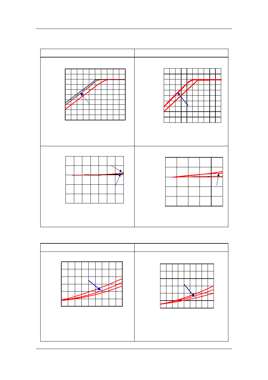
Typical Performance Characteristics
Output Voltage vs. Output Current
GS2911 (3.3V)
GS2911 (5V)
Topr=25
85
-40
5. 1
4. 7
4. 8
4. 9
5. 0
0 20 40 60 80 100 120 140 160 180
OUTPUT CURRENT: I
OUT
(mA)
VIN=6V
CIN=1
F(Tantalum), CL=1 F(Tantalum)
OU
T
P
UT
VO
LT
AG
E:VO
UT
(
V
)
3. 4
3. 3
3. 2
3. 1
3. 0
0 20 40 60 80 100 120 140 160 180
Topr =25
- 30
80
VIN=4.3V
CIN=1
F(Tantalum), CL=1 F(Tantalum)
Output Current IOUT (mA)
Ou
tp
ut Vo
ltag
e:VOUT
(V)
GS2911 Globaltech Semiconductor
www.globaltechsemi.com 6 GS2911
Output Voltage vs. Input Voltage
GS2911 (3.3V)
GS2911 (5V)
Input/Output Voltage Differential vs. Output Current
GS2911 (3.3V)
GS2911 (5V)
0 20 40 60 80 100120140160180
-0.2
0.0
0.2
0.4
0.6
0.8
1.0
Topr=25
85
-40
CIN=1 F(Tantal um), CL=1 F(Tantal um)
OUTPUT CURRENT : I
OUT
(mA)
I
N
PUT/
OUTPUT VOLTAGE
DIFF. :V
d
i
f (V)
0 20 40 60 80 100 120 140 160 180
- 0. 2
0. 0
0. 2
0. 4
0. 6
0. 8
1. 0
CIN=1
F(Tantalum), CL=1 F(Tantalum)
OUTPUT CURRENT : I
OUT
(mA)
I
N
PUT/
OUTPUT VOLTAGE
DIFF. :V
d
i
f (V)
Topr =25
80
-30
10mA
40mA
IOUT=1mA
2. 8
3. 3
3. 8
Input Voltage VIN(V)
O
u
t
pu
t
V
o
lt
age
VOUT(V)
2. 5
2. 7
2. 9
3. 1
3. 3
3. 5
Topr=25
CIN=1
F(Tantalum), CL=1 F(Tantalum)
10mA
40mA
IOUT=1mA
5.2
5.0
4.8
4.6
4.4
4.2
4.5
5.0
5.5
Topr=25
CIN=1 F(Tantal um), CL=1 F(Tantal um)
INPUT VOLTAGE : V
IN
(V)
OUT
P
UT VOLTAGE :
V
OUT
(V
)
10mA
40mA
IOUT=1mA
5
6
7
8
9
10
4.85
4.90
4.95
5.00
5.05
5.10
INPUT VOLTAGE:V
IN
(V)
OU
TP
UT V
O
LTAGE:V
OUT
(V)
Topr=25
CIN=1
F(Tantalum), CL=1 F(Tantalum)
40mA
IOUT=1mA,10mA
3
4
5
6
7
8
9
10
3. 15
3. 20
3. 25
3. 30
3. 35
3. 40
Input Voltage VIN (V)
Topr=25
CIN=1
F(Tantalum), CL=1 F(Tantalum)
O
u
tp
ut Voltage VO
UT (
V
)

GS2911 Globaltech Semiconductor
www.globaltechsemi.com 7 GS2911
Supply Current vs. Input Voltage
GS2911 (3.3V)
GS2911 (5V)
Load Transient Response
GS2911 (3.3V)
GS2911 (5V)
0
2
4
6
8
10
0
1
2
3
INPUT VOLTAGE:V
IN
(V)
SUPPLY CURR
ENT
:Is
s(
A)
Topr =25
85
- 40
Topr=25
80
-30
3
4
5
6
7
8
9 10
1.50
1.75
2.00
2.25
2.50
Input Voltage VIN(V)
Supply Current
Iss(
A)
TIME(2msec/div)
2
3
4
5
6
7
0
40
80
120
160
200
OU
TPUT VOLTAGE:V
OU
T
(V)
OUTPUT C
URRENT:I
OUT
(mA)
VIN=6V, CL=1
F(Tantalum)
Output Voltage
Output Current
40mA
1mA
TIME(2msec/div)
0.3
1.3
2.3
3.3
4.3
5.3
0
40
80
120
160
200
OUTPUT VOLTAGE:V
OU
T
(V)
OUTPUT CURRENT:
I
OU
T
(mA)
VIN=4.3V, CL=1
F(Tantalum)
Output Voltage
Output Current
40mA
1mA
GS2911 Globaltech Semiconductor
www.globaltechsemi.com 8 GS2911
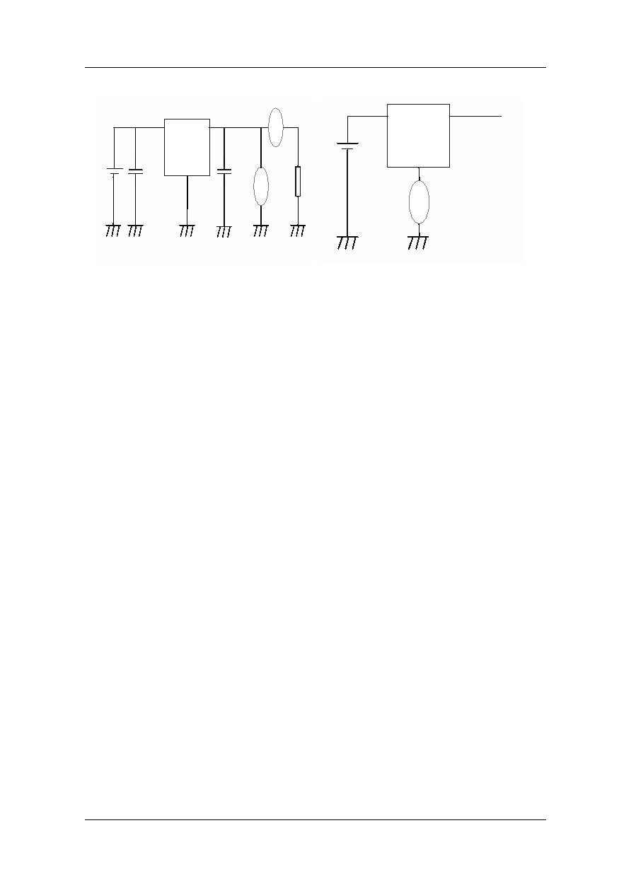
Typical Application Circuits
Vin
1uF
(Trantalum)
1uF
(Trantalum)
Vin
Vout
Vss
V
A
Vin
Vout
Vss
Vin
A
Open
Notes on Use
1. There is a possibility that oscillation may occur as a result of the impedance present
between the power supply and the IC's input. Where impedance is 10
or more, please
use a capacitor (C
IN
) of at least 1µF. With a large output current, operations can be
stabilised by increasing capacitor size (C
IN
). If C
IN
is small and capacitor size (CL) is
increased, there is a possibility of oscillation due to input impedance. In such cases, either
increasing the size of C
IN
or decreasing the size of CL can stabilize operations.
2. Please ensure that output current (I
OUT
) is less than P
D
+ (V
IN
- V
OUT
) and does not exceed
the stipulated Continuous Total Power Dissipation value (P
D
).
3.
Should you wish to increase output current (I
OUT
) and/or have the capability to exceed the
stipulated P
D
value, using a current boost circuit (similar to the one shown below) is likely
to lead to oscillation. With such applications, we recommend use of a boost type voltage
regulator, such as the GS2911 series.
GS2911 Globaltech Semiconductor
www.globaltechsemi.com 9 GS2911
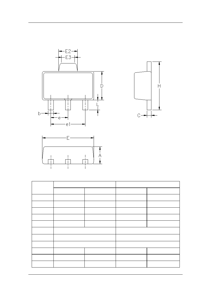
Package Dimension
SOT-89 PLASTIC PACKAGE
Dimensions In Millimeters
Dimensions In Inches
Symbol
Min Max Min Min
A 1.450 1.550 0.570 0.061
b 0.440 0.480 0.017 0.019
C 0.360 0.400 0.014 0.016
E 4.450 4.550 0.175 0.179
E2 1.500 1.700 0.059 0.067
E3 1.400Ref
0.055Ref
e 1.500BSC
0.059BSC
e1 3.000BSC
0.118BSC
H 4.150 4.250 0.163 0.167
D 2.450 2.550 0.096 0.100
L 0.900 1.100 0.035 0.043
GS2911 Globaltech Semiconductor
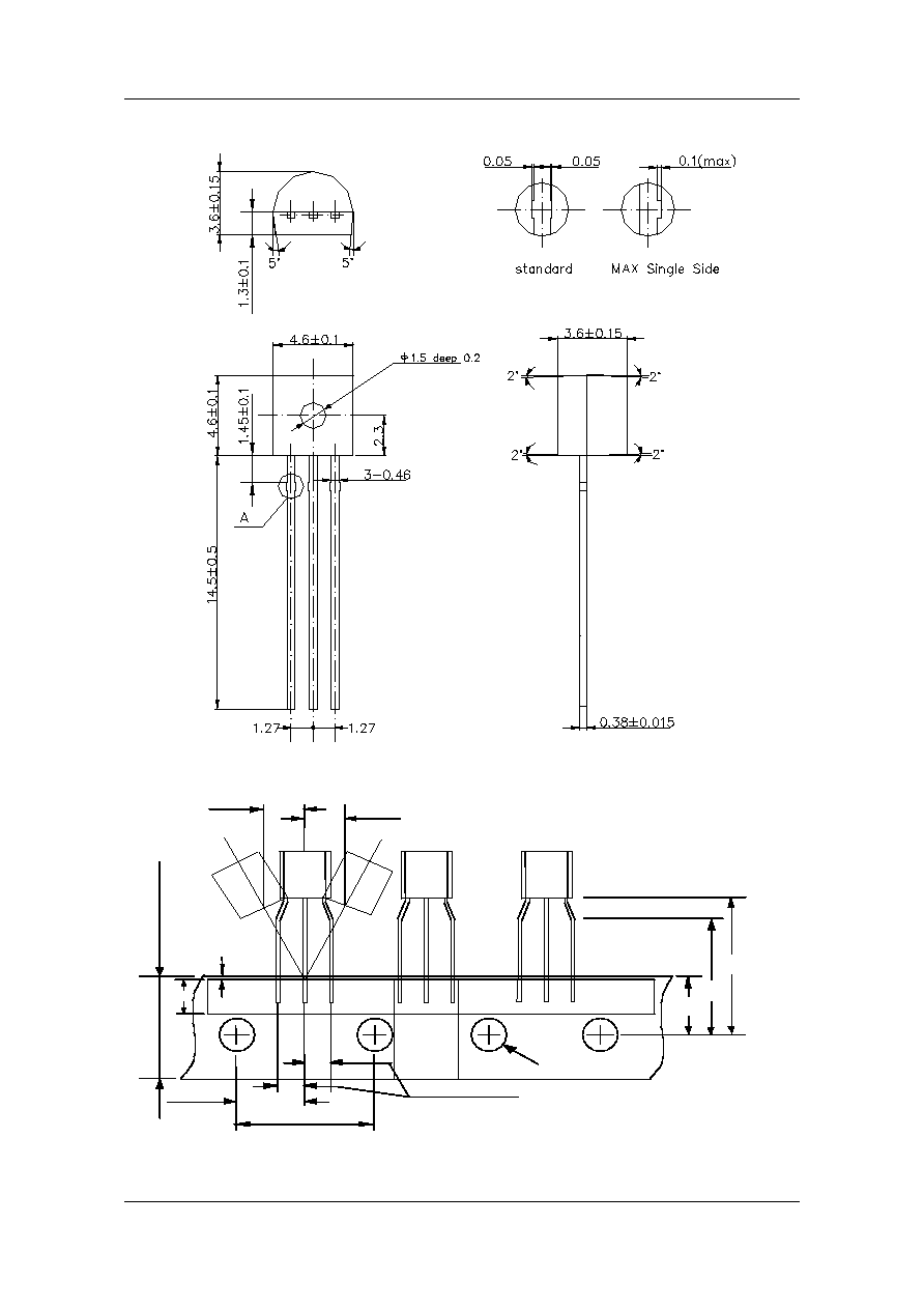
www.globaltechsemi.com 10 GS2911
TO-92 PLASTIC PACKAGE
0+1.0
0+1.0
21.0max
16±0.5
9.0+0.5
4.0±0.2
12.7±0.3
6.35±0.5
2.5+0.4 or 2.5-0.1
1.0max
6.0±0.5
18.0+1.6 or
18.0-
0.5

GS2911 Globaltech Semiconductor
www.globaltechsemi.com 11 GS2911
Information furnished is believed to be accurate and reliable. However Globaltech Semiconductor
assumes no responsibility for the consequences of use of such information nor for any infringement of
patents or other rights of third parties, which may result from its use. No license is granted by implication
or otherwise under any patent or patent rights of Globaltech Semiconductor. Specifications mentioned in
this publication are subject to change without notice. This publication supersedes and replaces all
information without express written approval of Globaltech Semiconductor.