 | ÐлекÑÑоннÑй компоненÑ: GS75232S | СкаÑаÑÑ:  PDF PDF  ZIP ZIP |
Äîêóìåíòàöèÿ è îïèñàíèÿ www.docs.chipfind.ru
www.globaltechsemi.com 1 GS75232
GS75232
Multiple RS-232 Drivers & Receivers
Product Description
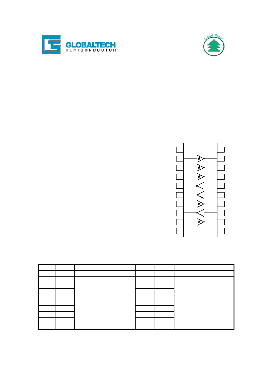
The GS75232 are monolithic device containing 3 independent drives and 5
receivers. These are designed to interface between date terminal equipment and
date communication equipment as designed by EIA-232-D.
Features
n
Meets standard EIA-232-D (Revision of RS-232-C)
n
Drivers
- Current Limited Output : 10 mA Typical
- Power-off Output Impedance : 300
Min
- Slew Rate Control by Load Capacitor
- Flexible Supply Voltage Range
- Input Compatible with Most TTL and DTL Circuits
n
Receivers
- Input Resistance : 3 k
to 7 k
- Input Signal Range :
±
30 V
- Built-in Input Hysteresis (Double Threshold)
VCC+
VCC
VCC -
GND
RA1
RY1
RA2
RA3
RY2
RY3
DY1
DY2
DA1
DA2
RA4
RY4
RA5
RY5
DY3
DA3
GS75232
Pin Description
Name Pin No
Function
Name Pin No
Function
V
CC+
1
Driver Section Supply +
V
CC-
10
Driver Section Supply -
DA1
16
DY1
5
DA2
15
DY2
6
Driver Output
DA3
13
Driver Input
DY3
8
V
CC
20
Receiver Section Supply
GND
11
Ground
RA1
2
RY1
19
RA2
3
RY2
18
RA3
4
Receiver Input
RY3
17
Receiver Output
RA4
7
RY4
14
RA5
9
RY5
12
GS75232 Globaltech Semiconductor
www.globaltechsemi.com 2 GS75232
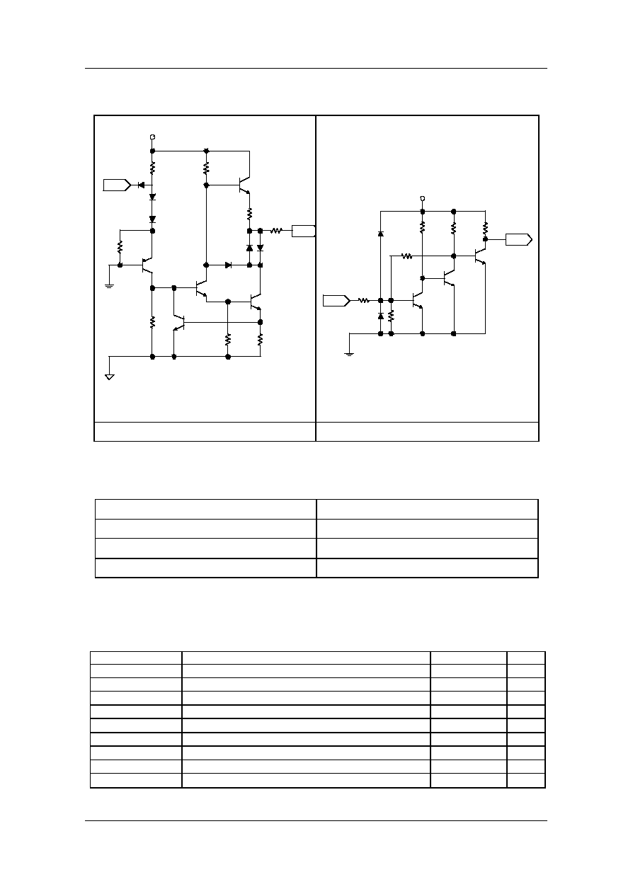
Representative Schematic Diagram
DA
DY
VCC+
VCC
-
8K2
3K6
10K
7K
70
70
6K2
300
DA
DY
2K
5K
9K
2K
10K
4K
VCC
Driver
Receiver
Ordering Information
Device
Package
GS75232S
SOIC-20
GS75232SS
SSOP-20
GS75232TS
TSSOP-20
"F" means Lead Free part.
*Request for other voltages, please contact factory directly.
Absolute Maximum Ratings
Symbol
Parameter
Rating
Unit
V
CC+
Supply Voltage
15
V
V
CC-
Supply Voltage
-15
V
V
CC
Supply Voltage
10
V
VI (Driver)
Input Voltage
-15 to +7
V
VI (Reciver)
Input Voltage
±
30
V
VO (Driver)
Output Voltage
-15 to +15
V
PT
Continuous Power Dissipation (Below 25
o
C)
1.0
W
T
STG
Storage Temperature
-65 to +175
o
C
Top
Operating Temperature
0 to +75
o
C
GS75232 Globaltech Semiconductor
www.globaltechsemi.com 3 GS75232
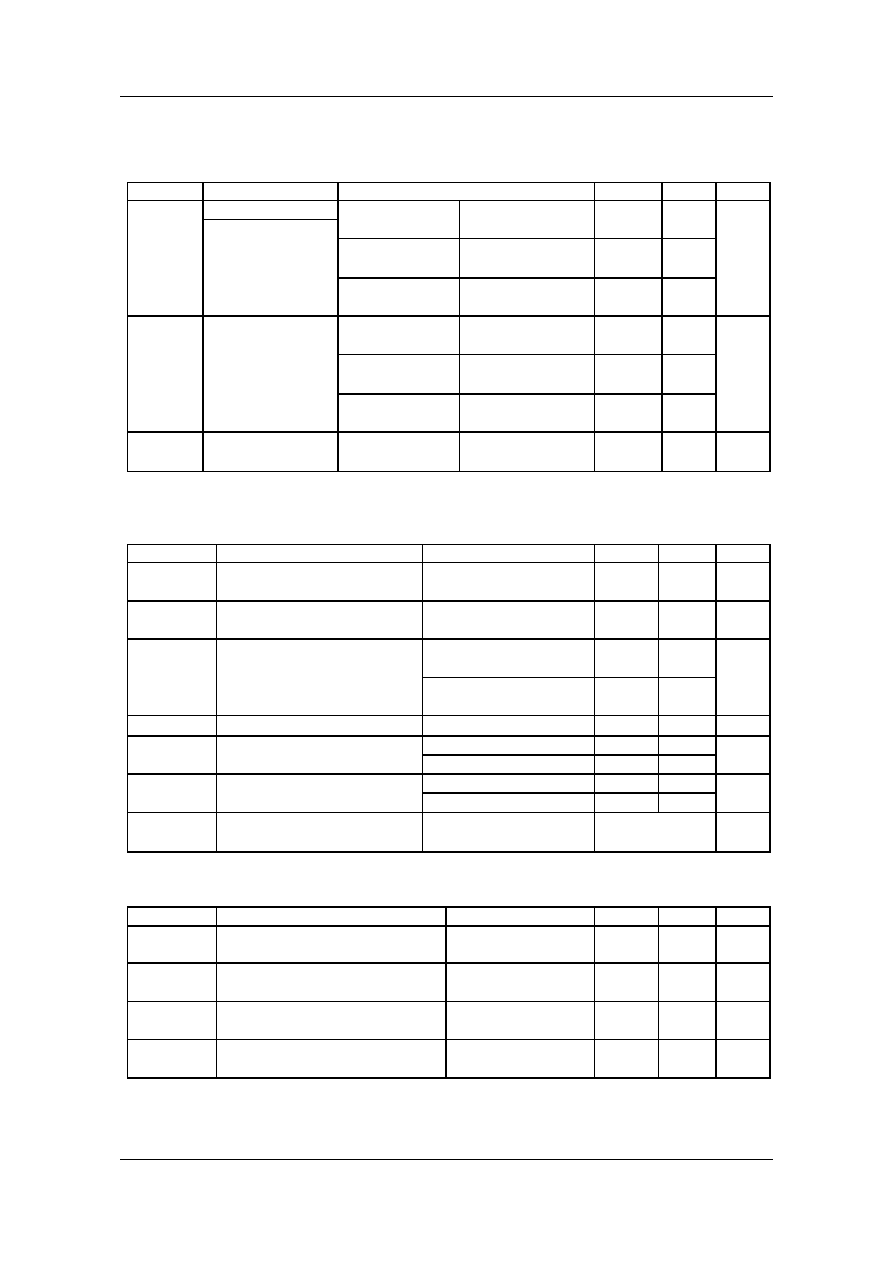
Electrical Characteristics
Supply Current
(V
CC
= 5V, T
A
= 25
O
C)
Symbol Parameter
Test Condition
Min
Max
Unit
I
CC+
Supply Current V
CC+
= 9 V
V
IN
= 1.9V
15
mA
from V
CC+
No Load
V
IN
= 0.8V
-
4.5
V
CC+
= 12 V
V
IN
= 1.9V
19
No Load
V
IN
= 0.8V
-
5.5
V
CC+
= 15 V
V
IN
= 1.9V
25
No Load
V
IN
= 0.8V
-
9
I
CC-
Supply Current V
CC-
= -9 V
V
IN
= 1.9V
-15
mA
from V
CC-
No Load
V
IN
= 0.8V
-
-3.2
V
CC-
= -12 V
V
IN
= 1.9V
-19
No Load
V
IN
= 0.8V
-
-3.2
V
CC-
= -15 V
V
IN
= 1.9V
-25
No Load
V
IN
= 0.8V
-
-3.2
I
CC
Supply Current
mA
from V
CC
V
CC
= 5 V
V
IN
= 5.0V
-
30
Receiver Section
Symbol
Parameter
Test Conditions
Min
Max
Unit
Positive-Going
VT+
Threshold Voltage
1.75
2.25
V
Negative-Going
VT-
Threshold Voltage
0.75
1.25
V
V
I
= 0.75V,
I
OL
=-0.5mA
2.6
5
Input Open,
V
OH
High Level Output
Voltage
I
OL
= -0.5 mA
2.6
5
V
V
OL
Low Level Output Voltage V
I
= 3V, I
OL
= 10 mA
-
0.45
V
V
I
= 25V
3.6
8.3
I
IH
High-Level Input Current
V
I
= 3V
0.43
-
mA
V
I
= -25V
-3.6
-8.3
I
IL
Low-Level Input Current
V
I
= -3V
-0.43
-
mA
Short-Circuit
-3
I
OS
Output Current
(tip)
mA
Receiver Switching Characteristic
(V
CC
= 5V)
Symbol
Parameter
Test Conditions
Min
Max
Unit
t
PLH
Propagation Delay Time,
Low-To-High-Level Output
C
L
= 15
F
R
L
= 3.9 k
-
150
ns
t
PHL
Propagation Delay Time,
High -To- Low -Level Output
C
L
= 15
F
R
L
= 390 k
-
50
ns
t
TLH
Transition Time,
Low-To-High-Level Output
C
L
= 15
F
R
L
= 3.9 k
-
175
ns
t
THL
Transition Time,
High -To- Low -Level Output
C
L
= 15
F
R
L
= 390 k
-
20
ns
GS75232 Globaltech Semiconductor
www.globaltechsemi.com 4 GS75232
Driver Section
Symbol
Parameter
Test Conditions
Min
Max
Unit
High Level
V
CC+
= 9 V
V
IH
Input Voltage
V
CC-
= -9 V
1.9
-
V
Low Level
V
IL
Input Voltage
-
0.8
V
V
CC+
= 9 V
V
CC-
= -9 V
6
-
V
V
CC+
= 13.2 V
V
OH
High Level
Output Voltage
V
IL
= 0.8V
RL = 3 k
V
CC-
= -13.2 V
9
-
V
CC+
= 9 V
V
CC-
= -9 V
-
-6
V
V
CC+
= 13.2 V
V
OL
Low Level
Output Voltage
V
IH
= 1.9V
RL = 3 k
V
CC-
= -13.2 V
-
-9
High Level
I
IH
Input Current
V
I
= 5V
-
10
µ
A
Low Level
I
IL
Input Current
V
I
= 0
-
-1.6
mA
Short Circuit
Output Current
I
OS(H)
at High Level
V
I
= 0.8V
V
O
= 0
-6
-12
mA
Short Circuit
Output Current
I
OS(L)
at Low Level
V
I
= 1.9V
V
O
= 0
6
12
mA
Output Resistance, V
CC+
= 0, V
CC-
= 0
R
O
Power Off
V
O
= -2V to 2V
300
-
Driver Switching Characteristic
(V
CC+
= 9V, V
CC-
= -9V T
A
= 25
O
C)
Symbol
Parameter
Test Conditions
Min
Max
Unit
t
PLH
Propagation Delay Time,
ns
Low-To-High-Level Output
-
500
t
PHL
Propagation Delay Time,
ns
High -To- Low -Level Output
-
175
t
TLH
Transition Time,
Low-To-High-Level Output
*
-
100
ns
t
THL
Transition Time,
High -To- Low -Level
Output*
RL = 3 k
CL = 15
µ
F
See Figure 1
-
75
ns
t
TLH
Transition Time,
Low-To-High-Level
Output**
2.5
(tip)
µ
s
t
THL
Transition Time,
High-To-Low -Level
Output**
RL = 3 k
to 7 k
CL = 2500
F
See Figure 1
3.0
(tip)
µ
s
*- Measured between 10 % and 90 % Points of Output Waveform
** - Measured between +3V and -3V Points on the Output Waveform (EIA-232-D
Condition)
GS75232 Globaltech Semiconductor
www.globaltechsemi.com 5 GS75232
Receiver Section
Symbol
Parameter
Test Conditions
Min
Max
Unit
Positive-Going
VT+
Threshold Voltage
1.75
2.25
V
Negative-Going
VT-
Threshold Voltage
0.75
1.25
V
V
I
= 0.75V,
I
OL
=-0.5mA
2.6
5
Input Open,
V
OH
High Level Output
Voltage
I
OL
= -0.5 mA
2.6
5
V
V
OL
Low Level Output Voltage V
I
= 3V, I
OL
= 10 mA
-
0.45
V
V
I
= 25V
3.6
8.3
I
IH
High-Level Input Current
V
I
= 3V
0.43
-
mA
V
I
= -25V
-3.6
-8.3
I
IL
Low-Level Input Current
V
I
= -3V
-0.43
-
mA
Short-Circuit
-3
I
OS
Output Current
(tip)
mA
Receiver Switching Characteristic (V
CC
= 5V)
Symbo
l
Parameter
Test Conditions
Min
Max
Unit
t
PLH
Propagation Delay Time,
Low-To-High-Level Output
C
L
= 15
F
R
L
= 3.9 k
-
150
ns
t
PHL
Propagation Delay Time,
High -To- Low -Level Output
C
L
= 15
F
R
L
= 390 k
-
50
ns
t
TLH
Transition Time,
Low-To-High-Level Output
C
L
= 15
F
R
L
= 3.9 k
-
175
ns
t
THL
Transition Time,
High -To- Low -Level Output
C
L
= 15
F
R
L
= 390 k
-
20
ns
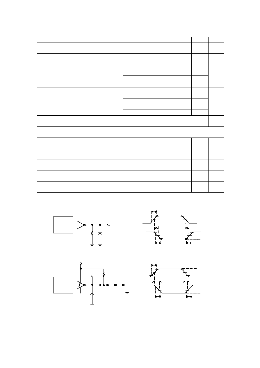
Typical Performance Characteristics
PULSE
GENERATOR
(See Note A)
OUTPUT
RECEIVER
C
L
R
L
PULSE
GENERATOR
(See Note A)
OUTPUT
DRIVER
C
L
R
L
INPUT
OUTPUT
3V
0V
V
OH
V
OL
1.5V
1.5V
10ns
50%
50%
t
THL
t
TLH
t
PLH
t
PLH
Voltage Waveform
INPUT
OUTPUT
3V
0V
V
OH
V
OL
50%
50%
10ns
1.5V
1.5V
t
THL
t
TLH
t
PLH
t
PLH
10%
10%
90%
90%
Tw=20us, Voltage Waveform
Note A. The pulse generator has the following characteristics. f = 200 KHz, Z
O
= 50
B. C included probe and jig capacitance.
C. All diodes are 1N3064 or equivalent.
Fig1. Propagation and Transition Times
GS75232 Globaltech Semiconductor
www.globaltechsemi.com 6 GS75232
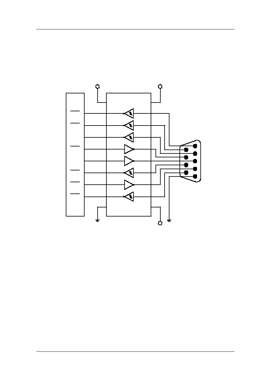
Applications Information
1
2
3
4
5
6
7
8
9
-12V
+12V
+5V
UART
DCD
DSR
RTS
S OUT
CTS
S IN
DTR
RI
RS-232
DB-9
Connector
SIO Card
GS75232 Globaltech Semiconductor
www.globaltechsemi.com 7 GS75232
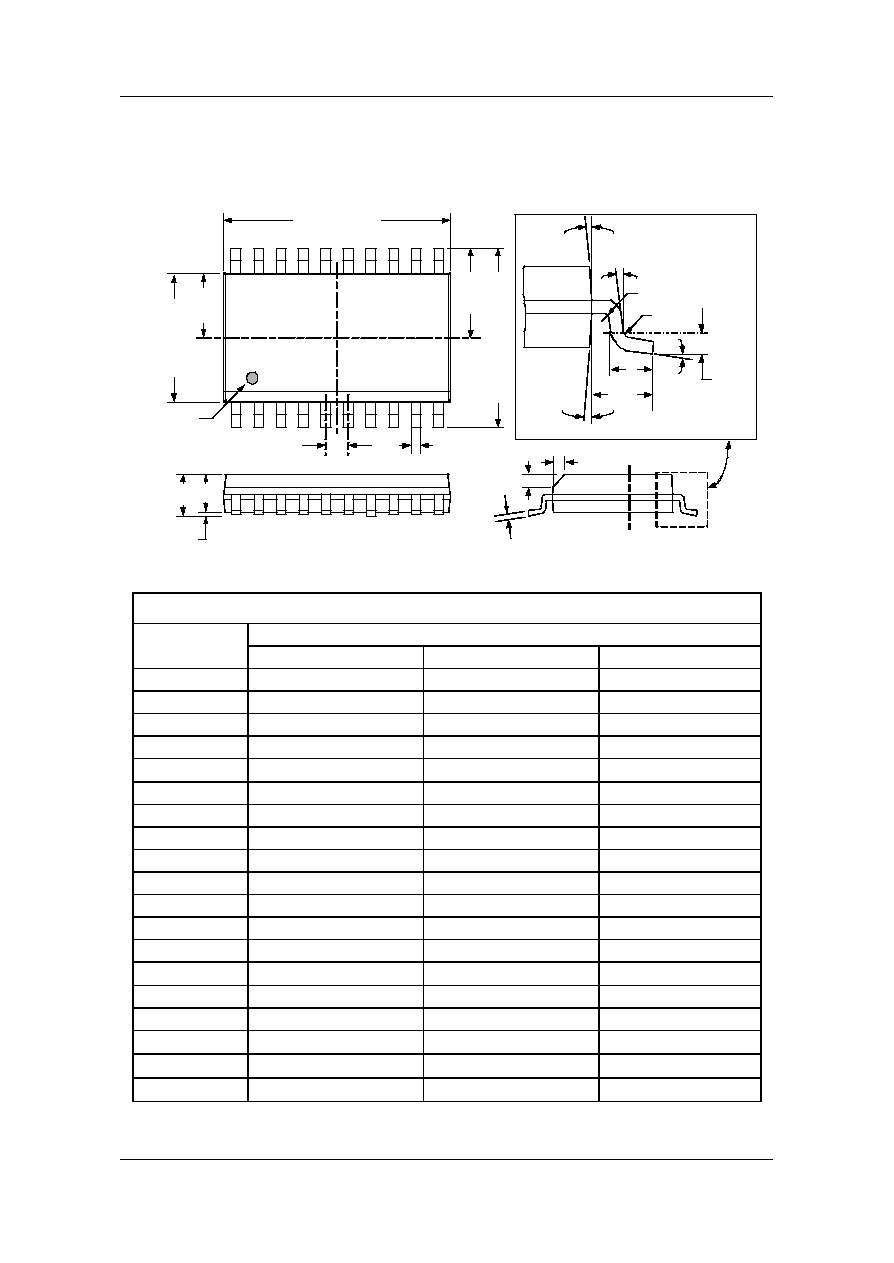
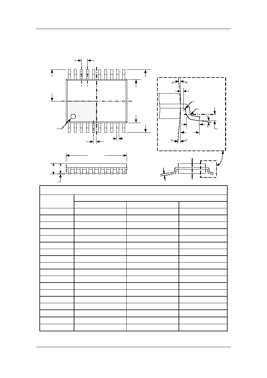
Package Dimensions
SOIC-20L
A1
A A2
E1/2
E1
D
e
b
E
E/2
PIN 1
MARKING
c
h
R1
R
GAUGE
PLANE
L2
1
2
1
+
L1
L
Dimensions
Millimeters
SYMBOL
MIN
TYP
MAX
A
2.35
-
2.65
A1
0.10
-
0.30
A2
2.05
-
2.55
b
0.31
-
0.51
b1
0.27
-
0.48
c
0.20
-
0.33
D
-
12.80
-
E
-
10.30
-
E1
-
7.50
-
e
-
1.27
-
L
0.40
-
1.27
L1
-
1.40
-
L2
-
0.25
-
R
0.07
-
-
R1
0.07
-
-
h
0.25
-
0.75
u
08
-
88
u1
58
-
158
u2
08
-
-
GS75232 Globaltech Semiconductor
www.globaltechsemi.com 8 GS75232
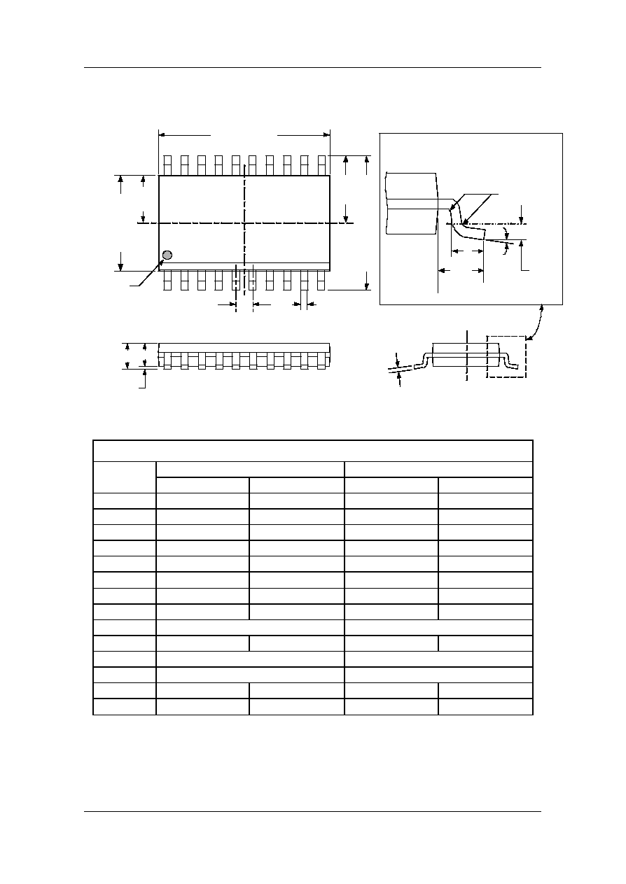
SSOP-20L
A1
A A2
E1/2
E1
D
e
b
E
E/2
PIN 1
MARKING
c
R
GAUGE
PLANE
L2
L1
L
SEATING
PLANE
Dimensions
Millimeters
Inches
SYMBOL
MIN
MAX
MIN
MAX
A
-
2.0
-
.078
A1
0.05
-
.002
-
A2
1.65
1.85
.065
.073
b
0.22
0.38
.008
.015
c
0.09
0.25
.003
.010
D
6.90
7.50
.271
.295
E
7.40
8.20
.290
.323
E1
5.00
5.60
.197
.220
e
0.65 (TYP)
.026 (TYP)
L
0.55
0.95
.021
.037
L1
1.25 (TYP)
.050 (TYP)
L2
0.25 (TYP)
.010 (TYP)
R
0.09
-
.003
-
u
08
88
08
88
GS75232 Globaltech Semiconductor
www.globaltechsemi.com 9 GS75232
TSSOP-20L
A1
A A2
D
e
b
E
E/2
c
R1
R
GAUGE
PLANE
L2
1
2
3
e / 2
1 2 3
E1
PIN 1
MARKING
L1
L
+
S
20
10
11
Dimensions
Millimeters
SYMBOL
MIN
TYP
MAX
A
-
-
1.20
A1
0.05
-
0.15
A2
0.80
1.00
1.05
b
0.19
-
0.30
b1
0.19
0.22
0.25
c
0.09
-
0.20
D
6.40
6.50
6.60
E
-
6.40
-
E1
4.30
4.40
4.50
e
-
0.65
-
L
0.45
0.60
0.75
L1
-
1.00
-
R
0.09
-
-
R1
0.09
-
-
S
0.20
-
-
u1
08
-
88
u2
-
128
-
u3
-
128
-

GS75232 Globaltech Semiconductor
www.globaltechsemi.com 10 GS75232
Notice
Information furnished is believed to be accurate and reliable. However Globaltech
Semiconductor assumes no responsibility for the consequences of use of such
information nor for any infringement of patents or other rights of third parties,
which may result from its use. No license is granted by implication or otherwise
under any patent or patent rights of Globaltech Semiconductor. Specifications
mentioned in this publication are subject to change without notice. This publication
supersedes and replaces all information without express written approval of
Globaltech Semiconductor.
(Revise Date:2005/10/26 Version_A1)