EM MICROELECTRONIC-MARIN SA
H6061
1
3 V Self Recovering Watchdog
Features
n
Watchdog fully operational from 2.7 to 5.25 V
n
Regulated DC voltage monitor, internal voltage
reference
n
Self recovering watchdog function: reset goes active
after the 1st timeout period, reset goes inactive
again after the 2nd timeout period, repeated active
reset signal until the system recovers
n
Standard timeout period and power-on reset time
(100 ms), externally programmable from 3 ms to
3 mins if required
n
Works down to 1.6 V supply voltage
n
Low voltage alarm prior to reset on power-down
n
Reset outputs of both polarities
n
Open drain outputs
n
Small footprint SO8 and DIP8 packages
Description
The H6061 is a combined initialiser, watchdog and
voltage monitor. The circuit is a low voltage low power
monolithic CMOS device combining a series of voltage
comparators and a programmable timer on the same
chip. The device is specially suited to
telecommunications applications where 3 V working is
expected, for functions such as supply voltage and
microprocessor monitoring. The reset outputs are self
recovering after a watchdog timeout, enabling the circuit
to work with standalone systems without any external
push-switch or control signal to restart after a watchdog
timeout. The circuit provides a reset signal of both
polarities. The state of the outputs is defined down to
1.6 V. An internal debouncer ensures power-up
perfomance for fast-rise supply lines.
Applications
n
Microprocessor and microcontroller systems
n
Point of sales equipment
n
Telecom products
n
Automotive subsystems
n
Microcontroller 68HC05 applications
Typical Operating Configuration
Pin Assignment
DIP8 / SO8
V
IN
V
SS
RC
TCL
V
DD
RES
SAVE
RES
Fig. 2
H6061
Fig. 1
V
IN
H6061
TCL SAVE
RES
V
DD
RES
V
SS
5 V
GND
NMI
RES
I/O
�
P
H6061
2
Absolute Maximum Ratings
Parameter
Symbol
Conditions
Voltage V
DD
to V
SS
Voltage at any pin to V
SS
Voltage at any pin to V
DD
Voltage at V
IN
to V
SS
Current at any output
Storage temperature
Electrostatic discharge max.
to MIL-STD-833C method 3015
V
DD
V
MIN
V
MAX
V
INMAX
I
MAX
T
STO
V
Smax
-
0.3 to + 5.6 V
-
0.3
+ 0.3
+
12 V
�
10 mA
-
65 to
+
150
�
C
1000 V
Table 1
Stresses above these listed maximum ratings may cause
permanent damage to the device. Exposure beyond
specified operating conditions may affect device
reliability or cause malfunction.
Handling Procedures
This device has built-in protection against high static
voltages or electric fields; however, it is advised that
normal precautions be taken as for any other CMOS
component. Unless otherwise specified, proper
operation can only occur when all terminal voltages are
kept within the supply voltage range. Unused inputs
must always be tied to a defined logic voltage level.
Operating Conditions
Parameter
Symbol Min. Typ. Max. Units
Operating temperature
Industrial
Supply voltage
Monitored input voltage
RC-oscillator programm -
ing (see Fig. 15)
External capacitance
External resistance
T
A
V
DD
V
IN
C1
R1
-40
2.7
0
10
+85
5.25
12
1
�
C
V
V
�
F
k
Leakage
<
1
�
A
Table 2
Electrical Characteristics
V
DD
= 5.0 V, T
A
=
-
40 to +85
�
C , unless otherwise specified
Parameter
Symbol
Test Conditions
Min.
Typ.
Max.
Units
V
DD
activation threshold
V
DD
deactivation threshold
Supply current
Input V
IN
, TCL
Leakage current
TCL input low level
TCL input high level
Leakage on pins ,
, RES
O/P drive logic low
V
ON
V
OFF
I
DD
I
P
V
IL
V
IH
I
OLK
I
OL
I
OL
I
OL
T
A
= 25
�
C
T
A
= 25
�
C
RC open, TCL at V
DD
or V
SS
V
SS
<
V
IP
<V
DD
T
A
= 80
�
C
V
OUT
= V
DD
V
OL
= 0.4 V
V
DD
= 3.5 V; V
OL
= 0.4 V
V
DD
= 1.6 V; V
OL
= 0.4 V
2.3
2.4
4
2
80
V
ON
-
0.3
80
0.005
0.050
8
2.7
140
1
0.8
1
V
V
�
A
�
A
V
V
�
A
mA
mA
�
A
Table 3
V
IN
Surveillance
Voltage thresholds at T
A
= 25
�
C
Version No.
Thresholds
V
SH
V
SL
V
RL
at V
DD
Threshold Voltage
Tolerance
Threshold
Ratio*
Pin V
IN
Input
25
1.54 1.50 1.46
2.7 � 5.0 V
�
10
%
�
2%
100 M
* Threshold ratio defined as V
SH
/ V
SL
or V
SL
/ V
RL
.
Table 4
SAVE
RES
H6061
5
Pin Description
Pin Name
Function
1
V
IN
Voltage monitoring input
2
Timer clear input signal
3
RC
RC oscillator tuning input
4
V
SS
GND terminal
5
Reset output, open drain
6
Save output, open drain
7
RES
Positive reset output, open drain
8
V
DD
Positive supply voltage
Table 6
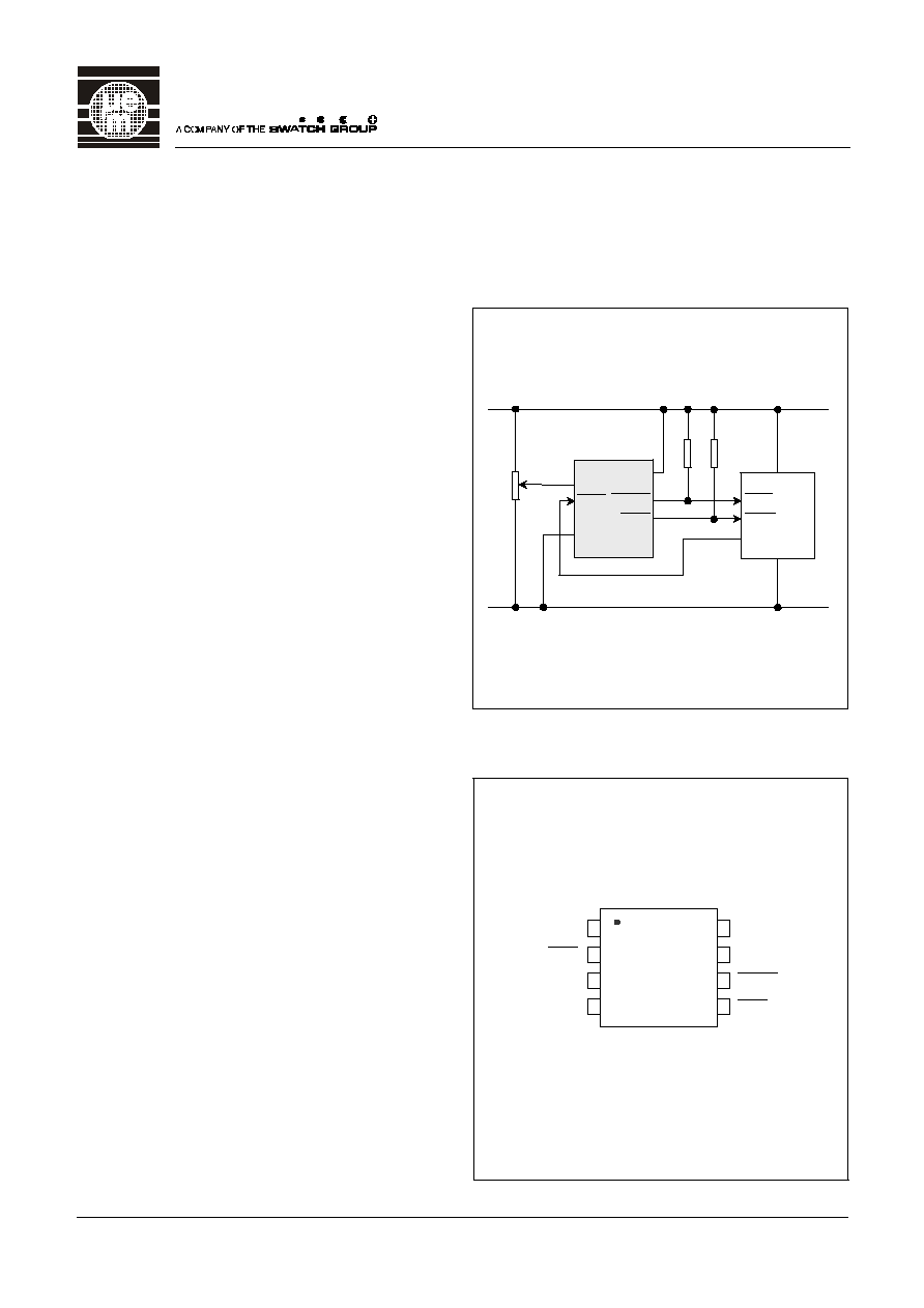
Functional Description
Thresholds and Outputs
The H6061 has open-drain outputs and voltage
thresholds on pin V
IN
of typically 1.5 V.
Internal Voltage Comparators
The voltage comparators detect the voltage applied to
pin V
IN
and compare it with thresholds V
SH
, V
SL
and V
RL
.
The H6061 is designed for monitoring regulated DC
voltages and has bandgap thresholds independent of
V
DD
. The reaction of the H6061 to voltage changes on
pin V
IN
is given in Fig. 4. During powering-up, the
outputs are active. After V
IN
reaches the V
SH
level, pin
SAVE deactivates after a short debounce time T
DB
to
allow for fast ramp-ups. The initialization time T
TO
then
passes before the two reset outputs go inactive.
Thereafter, when the voltage on pin V
IN
falls below the
V
SL
level, pin SAVE goes active low as a first warning. If
V
IN
then drops below the V
RL
level, the reset signals go
active and are guaranteed down to 1.6 V. The reset
outputs react also to timeouts (see "Timer clearing").
Note that when the supply voltage V
DD
is below the level
V
OFF
(about 2.2 V), all outputs are in the active state for
any allowed voltage of V
IN
.
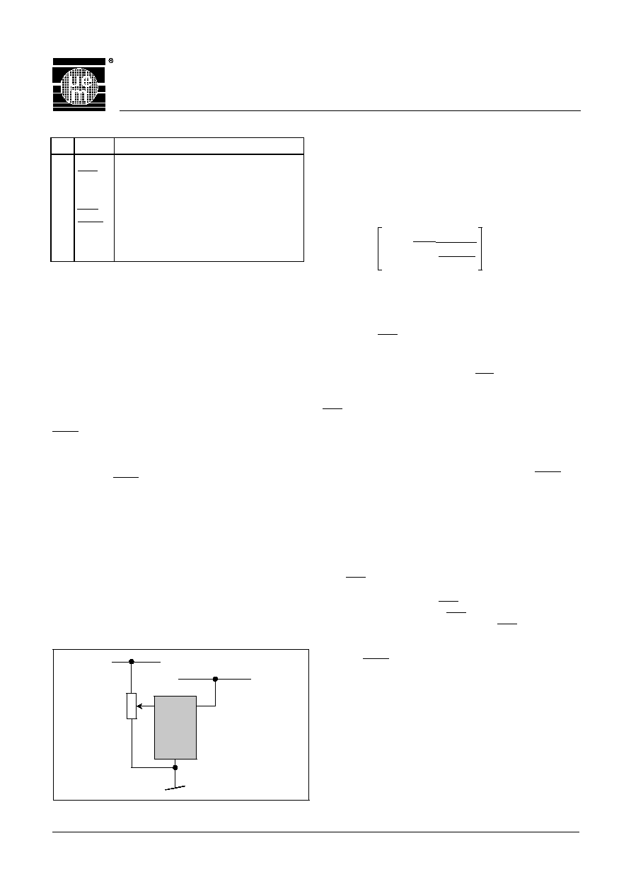
Voltage Programming
The H6061 was designed to give the best compromise
in normal usage (see Table 3). Its voltage threshold can
be programmed by an external resistor divider or a
potentiometer to react at proportionally higher voltage
levels (see Fig. 8 below).
Voltage Programming
Timer Programming
A single timeout period T
TO
is used for the initialization
reset duration and the watchdog timeout. With pin RC
unconnected, the on-chip RC oscillator and divider chain
give a timeout period T
TO
of typically 100 ms. A resistor
to V
DD
will shorten this time, and a capacitor to V
SS
will
lengthen it (see Fig. 11). An approximation for
calculating trial values given in milliseconds by the
formula:
R
1 min.
= 10 k
, C
1 max.
= 1
�
F
If R
1
is in M
and C
1
in pF, T
TO
will be in ms.
Choice of component values must be determined in
practice. To have a square wave of period 2T
TO
, simply
connect pin TCL to V
DD
or V
SS
and take the signal output
from a reset pin.
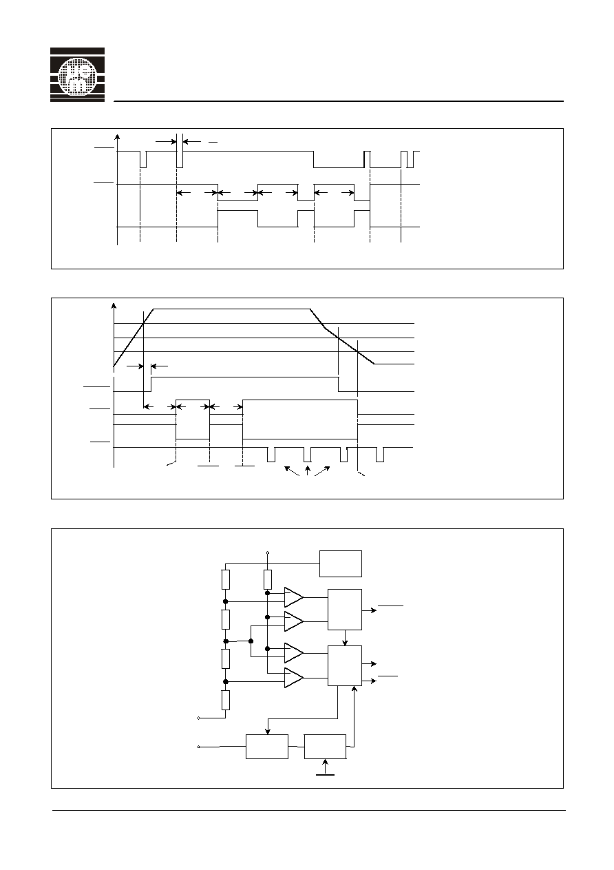
Timer Clearing
A negative edge or pulse at the TCL input longer than
150 ns will clear the timer and deactivate the reset
outputs under normal running conditions (see Fig. 3).
TCL will however have no effect either when V
DD
<
V
OFF
or
during the initialization period before the deactivation of
the reset pins.
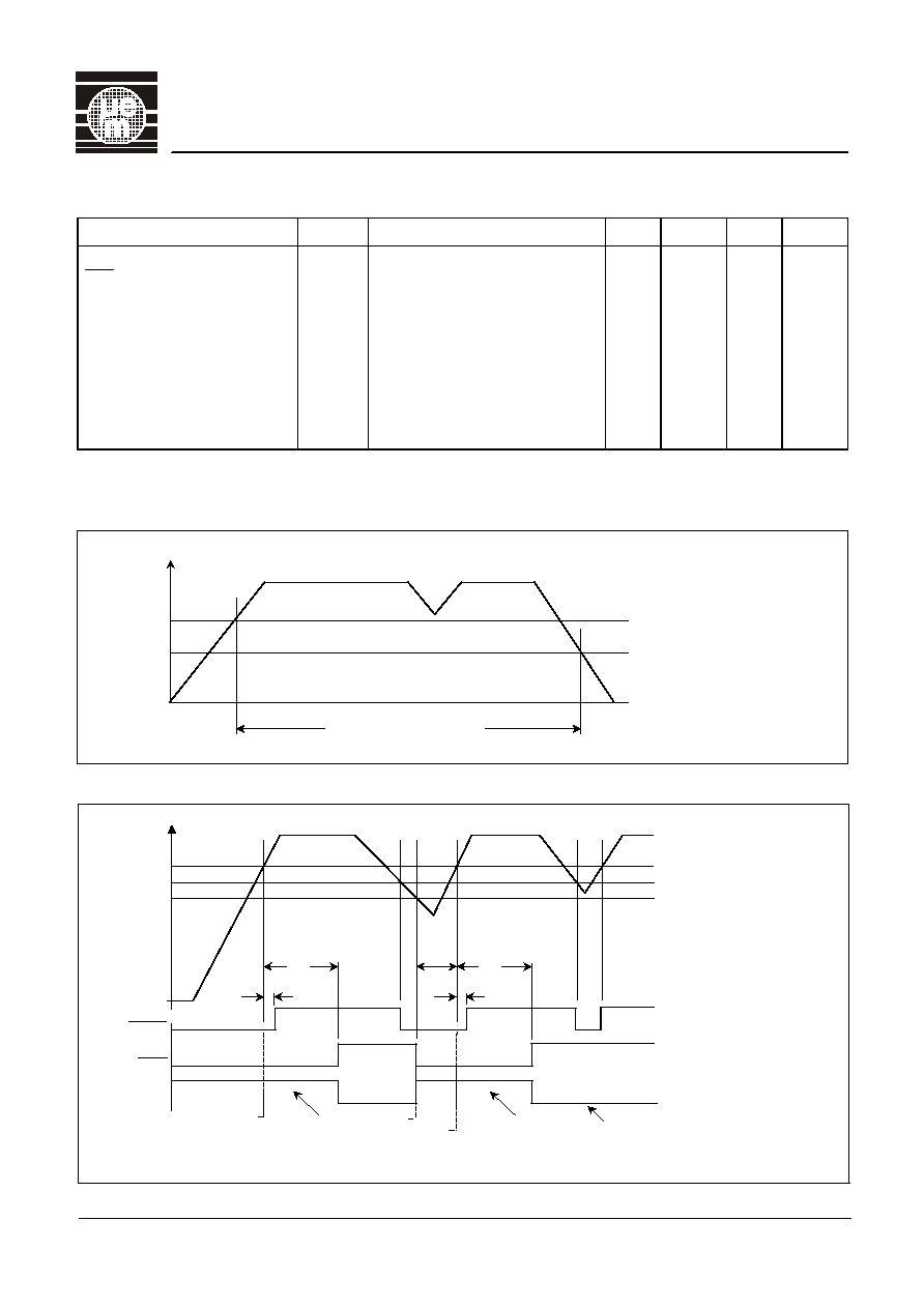
Combined Voltage and Timer Action
In Fig. 6 is a typical sequence of power-up, watchdog
run, and power-down. During initialization the SAVE pin
deactivates one debounce delay time T
DB
after V
IN
rises
above V
SH
, or when the power line V
DD
rises above V
ON
,
whichever happens last. The reset pins only deactivate
one timeout period T
TO
afterwards to free the watchdog
timer and end the initialization. Note that either V
IN
falling
below V
RL
threshold or V
DD
below V
ON
will cause an
initialization upon recovery. Following initialization, the
watchdog timer will time out after time T
TO
unless at least
one TCL pulse clears it. On timeout the reset pins
reactivate for a further T
TO
period before deactivating
again for another try. A TCL pulse will deactivate any
timeout reset, and another TCL pulse must follow within
a time T
TO
to keep reset inactive. If no TCL pulses come
at all, the reset pins go square-wave. Power-down
overrides all this however. A falling voltage on V
IN
gives a
warning SAVE = 0 signal at V
IN
= V
SL
before activating
the reset pins as soon as V
IN
drops below V
RL
. The
H6061 has fixed thresholds and low hysteresis for
monitoring regulated DC lines. Additional protection is
provided in case V
DD
supply falls over about 10% below
V
ON
which thereupon activates all outputs at once.
TCL
RES
SAVE
H6061
V
DD
+3 V / +5 V
V
IN
V
SS
Fig. 8
192
.
8
6
.
1
)
+
+
+
=
R
0.8
-
V
4.8
C
(32
0.75
1
DD
1
TO
T