 | –≠–ª–µ–∫—Ç—Ä–æ–Ω–Ω—ã–π –∫–æ–º–ø–æ–Ω–µ–Ω—Ç: H8250 | –°–∫–∞—á–∞—Ç—å:  PDF PDF  ZIP ZIP |

H8250 Megafunction
Universal Asynchronous
Receiver/Transmitter
CAST, Inc.
June 2002
Page 1
General Description
The H8250 is a standard UART providing 100%
software compatibility with the popular Intel 8250
device. It performs serial-to-parallel conversion on
data originating from modems or other serial
devices, and performs parallel-to-serial
conversion on data from a CPU to these devices.
Developed for easy reuse in Altera FPGA
applications, the H8250 is available optimized for
several device families with competitive utilization
and performance characteristics.
Symbol
A(2:0)
CS
RD
WR
MR
CLK
DIN(7:0)
RCLK
SIN
CTSn
DSRn
DCDn
RIn
DOUT(7:0)
SOUT
DDIS
RTSn
DTRn
OUT1n
OUT2n
INTR
BOUDOUTn
RXRDY
TXRDY
H8250
Features
∑
Capable of running all existing 8250 software
∑
Adds or deletes standard asynchronous
communication bits (start, stop and parity) to
or from the serial data
∑
Independently controlled transmit, receive,
line status and data set interrupts
∑
Programmable baud generator divides any
input clock by 1 to (2
16
- 1) and generates the
16 x clock
∑
Independent receiver clock input
∑
Modem control functions (CTSn, RTSn, DSRn,
DTRn, RIn, and DCDn)
∑
Fully programmable serial interface
characteristics:
o
5, 6, 7, or 8 bit characters
o
Even, odd, or no-parity bit generation and
detection
o
1, 1Ω, or 2 stop bit generation
o
Baud generation
∑
False start bit detection
∑
Complete status register
∑
Internal diagnostic capabilities: loopback
controls for communications link fault isolation
∑
Full prioritized interrupt system controls
Applications
∑
Serial or modem computer interface
∑
Serial interface within modems and other devices

CAST H8250 Megafunction Datasheet
CAST, Inc.
Page 2
Pin Description
Name Type
Polarity Description
MR
In
High
Master Reset (Asynchronous)
CLK
In
-
Master clock (Should be Global Signal)
RCLK
In
-
Receiver clock (Recommended as Global Signal)
RD In
High Read
control
WR
In
Falling
Write control (Recommended as Global Signal)
CS In
High Chip
Select
DIN[7:0]
In
-
Data Input Bus
CTSn In
Low Clear-to
-Send
DSRn
In
Low
Data Set Ready
DCDn
In
Low
Data Carrier Detect
SIN
In
-
Serial Input Data
RIn In
Low Ring
Indicator
A[2:0] In
-
Register
Select
DOUT[7:0]
Out
-
Data Output Bus
SOUT
Out
-
Serial Output Data
DDIS Out
High Driver
Disable
RTSn Out
Low Request-to-Send
DTRn
Out
Low
Data Terminal Ready
OUT1n Out
Low
Output
1
OUT2n Out
Low
Output
2
INTR Out
High Interrupt
pending
BAUDOUTn Out Low
Baud
Out
RXRDY
Out
Low
Receiver Ready to Receive Transmissions
TXRDY
Out
Low
Transmitter Ready to Transmit Data
Register Description
A(2:0)
Divisor *
Latch
Access Bit
Name Symbol
Default
(reset)
value
No.
bits
Read/
Write
0
0
Receiver Buffer Register
RBR
XX
8
R
0
0
Transmitter Holding Register
THR
XX
8
W
0
1
Divisor Latch (LSB)
DLR
01h
8
R/W
1
1
Divisor Latch (MSB)
DMR
00h
8
R/W
1
0
Interrupt Enable Register
IER
00h
8
R/W
2
X
Interrupt Identification Register
IIR
01h
8
R
3
X
Line Control Register
LCR
00h
8
R/W
4
X
Modem Control Register
MCR
00h
8
R/W
5
X
Line Status Register
LSR
60h
8
R
6
X
Modem Status Register
MSR
00h
8
R
7 X
Scratch
Register
SR 00h 8
R/W
*DLAB is the MSB of the Line Control Register
Switching Characteristics
Register Write
The Address (A) and Chip Select (CS) signals are not latched and therefore must be valid throughout the write
process. Writing is done at the falling edge of the WR signal.

CAST H8250 Megafunction Datasheet
CAST, Inc.
Page 3
A
valid
CS
WR
DIN
valid
Register Read
The Address (A) and Chip Select (CS) signals are not latched and therefore must be valid throughout the read
process. The RD signal is active 1.
A
valid
CS
RD
DOUT
DDIS
valid
Write to Transmitter
The timing diagram below depicts the situation where the transmitter is in the process of transmitting a byte
which is made up of the Data, Parity and Stop bits. Once the byte is written into the Transmitter Holding
Register, the TXRDY signal goes into the off (or high) state. This means that the transmitter is ready for a
transfer. As the byte just written starts the transmission (with the Start bit) the TXRDY bit goes low showing
that the transmitter is ready for the next byte.
SOUT
WR
DATA
PARITY
STOP
START
TXRDY
Timing Information for Write Function

CAST H8250 Megafunction Datasheet
CAST, Inc.
Page 4
Read from Receiver
The timing diagram that follows depicts the situation where the receiver is in the process of receiving a byte
which is just coming up to the Stop bit. Once a proper Stop bit is received the Byte is placed in the Receiver
Buffer Register. This event is signaled to the processor by the RXRDY signal which goes inactive when a byte is
awaiting reading. The Receiver Buffer Register must be read before the next byte is received or else an error
will be generated.
SIN
RD
RXRDY
STOP
RCLK
Timing information for Read Function
Receiver Synchronization
When the Receiver detects a low state in the incoming data stream it will synchronize to it. After this start edge
the UART will wait 1.5*(the normal bit length). This causes the subsequent bits to be read at the middle of its
width. This figure depicts this synchronization process.
Start bit
Detected
Message
bit Read
Message
bit Read
First
Message bit
Second
Message bit
1.5 bits
Receiver Synchronization
CAST H8250 Megafunction Datasheet
CAST, Inc.
Page 5
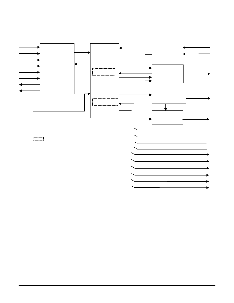
Block Diagram
A2-A0
CS
WR
RD
MR
CLK
DDIS
D7 ≠ D0
INTERFACE
REGISTERS
RXFIFO
TXFIFO
D7 ≠ D0
RXBLOCK
INTERRUPT
CONTROL
BAUD RATE
GENERATOR
TXBLOCK
SIN
RCLK
INTR
BAUDOUT
SOUT
= FIFO Mode
CTSn
DSRn
DCDn
RIn
DTRn
OUT1n
OUT2n
RTSn
RXRDY
TXRDY
Functional Description
As shown above and explained below, the H8250 includes six major blocks: Interface, Registers, RXBlock,
Interrupt Control, Baud Rate Generator, and TXBlock.
Interface
The Interface block is responsible for handling the communications with the processor (or parallel) side of the
system. All writing and reading of internal registers is accomplished through this block.
Registers
The Registers block holds all of the device's internal registers. See the Register Description table for details on
existing registers and their addresses. Some information comes from the other blocks, but this is all gathered
together in the Registers block and made available to all blocks.