
HAL525, HAL535
Hall Effect Sensor IC
Edition Aug. 30, 2000
6251-465-3DS
MICRONAS
MICRONAS

HAL525, HAL535
2
Micronas
Contents
Page
Section
Title
3
1.
Introduction
3
1.1.
Features
3
1.2.
Family Overview
4
1.3.
Marking Code
4
1.4.
Operating Junction Temperature Range
4
1.5.
Hall Sensor Package Codes
4
1.6.
Solderability
5
2.
Functional Description
6
3.
Specifications
6
3.1.
Outline Dimensions
6
3.2.
Dimensions of Sensitive Area
6
3.3.
Positions of Sensitive Areas
7
3.4.
Absolute Maximum Ratings
7
3.5.
Recommended Operating Conditions
8
3.6.
Electrical Characteristics
9
3.7.
Magnetic Characteristics Overview
14
4.
Type Description
14
4.1.
HAL525
16
4.2.
HAL535
18
5.
Application Notes
18
5.1.
Ambient Temperature
18
5.2.
Extended Operating Conditions
18
5.3.
Start-up Behavior
18
5.4.
EMC and ESD
20
6.
Data Sheet History
HAL525, HAL535
Micronas
3
Hall Effect Sensor Family
Release Note: Revision bars indicate significant
changes to the previous edition.
1. Introduction
The HAL 525 and HAL535 are Hall switches produced
in CMOS technology. The sensors include a tempera-
ture-compensated Hall plate with active offset com-
pensation, a comparator, and an open-drain output
transistor. The comparator compares the actual mag-
netic flux through the Hall plate (Hall voltage) with the
fixed reference values (switching points). Accordingly,
the output transistor is switched on or off.
The active offset compensation leads to magnetic
parameters which are robust against mechanical
stress effects. In addition, the magnetic characteristics
are constant in the full supply voltage and temperature
range.
The sensors are designed for industrial and automo-
tive applications and operate with supply voltages
from 3.8 V to 24 V in the ambient temperature range
from
-
40
∞
C up to 150
∞
C.
The HAL525 and HAL 535 are available in the
SMD-package SOT-89B and in the leaded version
TO-92UA.
1.1. Features
≠ switching offset compensation at typically 115 kHz
≠ operates from 3.8 V to 24 V supply voltage
≠ operates with static magnetic fields and dynamic
magnetic fields up to 10 kHz
≠ overvoltage protection at all pins
≠ reverse-voltage protection at V
DD
-pin
≠ magnetic characteristics are robust against
mechanical stress effects
≠ short-circuit protected open-drain output by thermal
shut down
≠ constant switching points over a wide supply voltage
range
≠ the decrease of magnetic flux density caused by ris-
ing temperature in the sensor system is compen-
sated by a built-in negative temperature coefficient
of the magnetic characteristics
≠ ideal sensor for window lifter, ignition timing, and
revolution counting in extreme automotive and
industrial environments
≠ EMC corresponding to DIN 40839
1.2. Family Overview
Both sensors have a latching behavior with typically
the same sensitivity. The difference between HAL 525
and HAL 535 is the temperature coefficient of the mag-
netic switching points.
Latching Sensors:
Both sensors have a latching behavior and requires a
magnetic north and south pole for correct functioning.
The output turns low with the magnetic south pole on
the branded side of the package and turns high with
the magnetic north pole on the branded side. The out-
put does not change if the magnetic field is removed.
For changing the output state, the opposite magnetic
field polarity must be applied.
Type
Switching
Behavior
Typical
Temperature
Coefficient
see
Page
525
latching
-
2000 ppm/K
14
535
latching
-
1000 ppm/K
16
HAL525, HAL535
4
Micronas
1.3. Marking Code
All Hall sensors have a marking on the package sur-
face (branded side). This marking includes the name
of the sensor and the temperature range.
1.4. Operating Junction Temperature Range
The Hall sensors from Micronas are specified to the
chip temperature (junction temperature T
J
).
A: T
J
=
-
40
∞
C to +170
∞
C
K: T
J
=
-
40
∞
C to +140
∞
C
E: T
J
=
-
40
∞
C to +100
∞
C
The relationship between ambient temperature (T
A
)
and junction temperature is explained in Section 5.1.
on page 18.
1.5. Hall Sensor Package Codes
Hall sensors are available in a wide variety of packag-
ing versions and quantities. For more detailed informa-
tion, please refer to the brochure: "Ordering Codes for
Hall Sensors".
1.6. Solderability
all packages: according to IEC68-2-58
During soldering reflow processing and manual
reworking, a component body temperature of 260
∞
C
should not be exceeded.
Components stored in the original packaging should
provide a shelf life of at least 12 months, starting from
the date code printed on the labels, even in environ-
ments as extreme as 40
∞
C and 90% relative humidity.
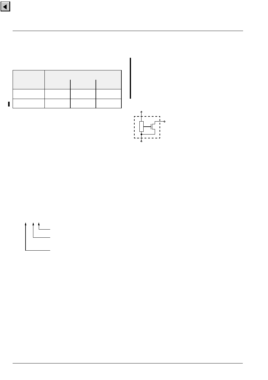
Fig. 1≠1: Pin configuration
Type
Temperature Range
A
K
E
HAL525
525A
525K
525E
HAL535
535A
535K
535E
HALXXXPA-T
Temperature Range: A, K, or E
Package: SF for SOT-89B
UA for TO-92UA
Type: 525 or 535
Example: HAL525UA-E
Type: 525
Package: TO-92UA
Temperature Range: T
J
=
-
40
∞
C to +100
∞
C
1 V
DD
2
GND
3
OUT
HAL525, HAL535
Micronas
5
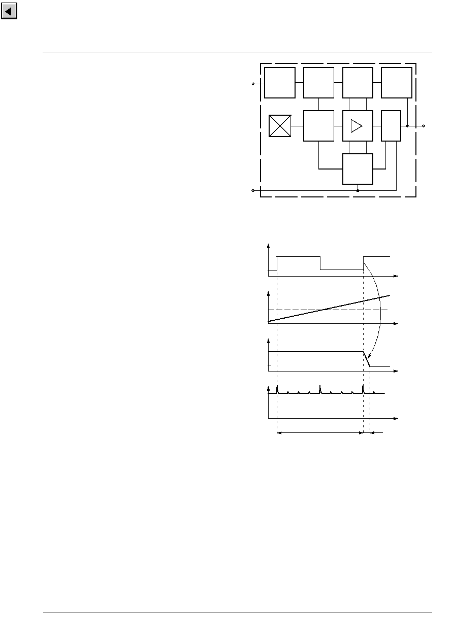
2. Functional Description
The Hall effect sensor is a monolithic integrated circuit
that switches in response to magnetic fields. If a mag-
netic field with flux lines perpendicular to the sensitive
area is applied to the sensor, the biased Hall plate
forces a Hall voltage proportional to this field. The Hall
voltage is compared with the actual threshold level in
the comparator. The temperature-dependent bias
increases the supply voltage of the Hall plates and
adjusts the switching points to the decreasing induc-
tion of magnets at higher temperatures. If the magnetic
field exceeds the threshold levels, the open drain out-
put switches to the appropriate state. The built-in hys-
teresis eliminates oscillation and provides switching
behavior of output without bouncing.
Magnetic offset caused by mechanical stress is com-
pensated for by using the "switching offset compensa-
tion technique". Therefore, an internal oscillator pro-
vides a two phase clock. The Hall voltage is sampled
at the end of the first phase. At the end of the second
phase, both sampled and actual Hall voltages are
averaged and compared with the actual switching
point. Subsequently, the open drain output switches to
the appropriate state. The time from crossing the mag-
netic switching level to switching of output can vary
between zero and 1/f
osc
.
Shunt protection devices clamp voltage peaks at the
Output-pin and V
DD
-pin together with external series
resistors. Reverse current is limited at the V
DD
-pin by
an internal series resistor up to
-
15 V. No external
reverse protection diode is needed at the V
DD
-pin for
reverse voltages ranging from 0 V to
-
15 V.
Fig. 2≠1: HAL525, HAL 535 block diagram
Fig. 2≠2: Timing diagram
Reverse
Voltage &
Overvoltage
Protection
Temperature
Dependent
Bias
Hysteresis
Control
Short Circuit
and
Overvoltage
Hall Plate
Switch
Comparator
Output
Clock
Protection
3
OUT
GND
2
1
V
DD
t
V
OL
V
OUT
1/f
osc
= 9
µ
s
V
OH
B
B
ON
f
osc
t
t
t
f
t
I
DD
t
HAL525, HAL535
6
Micronas
3. Specifications
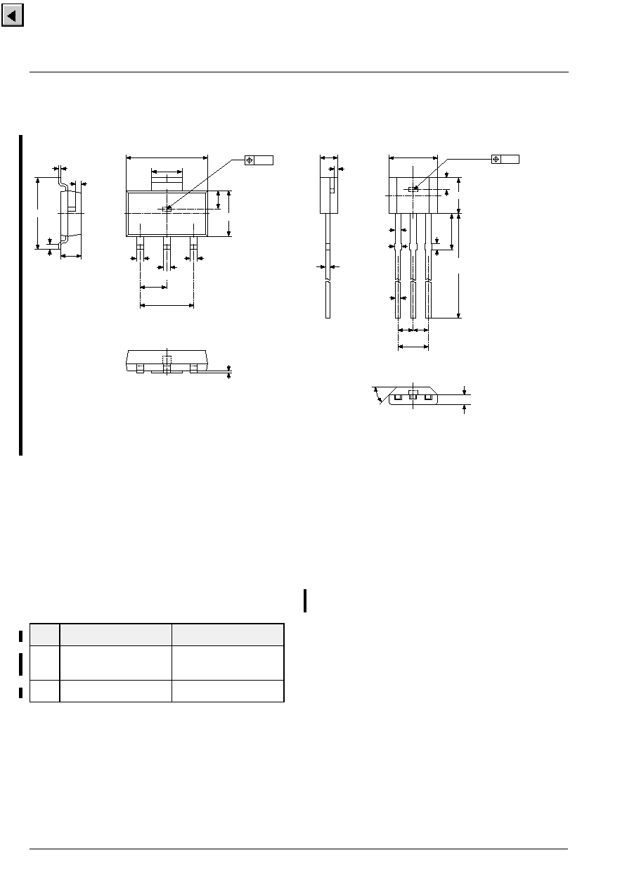
3.1. Outline Dimensions
Fig. 3≠1:
Plastic Small Outline Transistor Package
(SOT-89B)
Weight approximately 0.035 g
Dimensions in mm
3.2. Dimensions of Sensitive Area
0.25 mm
◊
0.12 mm
3.3. Positions of Sensitive Areas
Fig. 3≠2: Plastic Transistor Single Outline Package
(TO-92UA)
Weight approximately 0.12 g
Dimensions in mm
Note: For all package diagrams, a mechanical toler-
ance of
±
0.05 mm applies to all dimensions where no
tolerance is explicitly given.
The improvement of the TO-92UA package with the
reduced tolerances will be introduced end of 2001.
SOT-89B
TO-92UA
x
center of
the package
center of
the package
y
0.95 mm nominal
1.0 mm nominal
4.55
1.7
min.
0.25
2.55
0.4
0.4
0.4
1.5
3.0
0.06
±
0.04
branded side
SPGS0022-5-A3/2E
y
1
2
3
4
±
0.2
0.15
0.3
2
0.2
sensitive area
top view
1.15
0.75
±
0.2
3.1
±
0.2
0.55
branded side
0.36
0.8
0.3
45
∞
y
14.0
min.
1.27
1.27
2.54
1
2
3
0.42
1.5
4.06
±
0.1
3.05
±
0.1
0.48
SPGS7002-9-A/2E
0.4
sensitive area

HAL525, HAL535
Micronas
7
3.4. Absolute Maximum Ratings
Stresses beyond those listed in the "Absolute Maximum Ratings" may cause permanent damage to the device. This
is a stress rating only. Functional operation of the device at these or any other conditions beyond those indicated in
the "Recommended Operating Conditions/Characteristics" of this specification is not implied. Exposure to absolute
maximum ratings conditions for extended periods may affect device reliability.
3.5. Recommended Operating Conditions
Symbol
Parameter
Pin Name
Min.
Max.
Unit
V
DD
Supply Voltage
1
-
15
28
1)
V
-
V
P
Test Voltage for Supply
1
-
24
2)
-
V
-
I
DD
Reverse Supply Current
1
-
50
1)
mA
I
DDZ
Supply Current through
Protection Device
1
-
200
3)
200
3)
mA
V
O
Output Voltage
3
-
0.3
28
1)
V
I
O
Continuous Output On Current
3
-
50
1)
mA
I
Omax
Peak Output On Current
3
-
250
3)
mA
I
OZ
Output Current through
Protection Device
3
-
200
3)
200
3)
mA
T
S
Storage Temperature Range
-
65
150
∞
C
T
J
Junction Temperature Range
-
40
-
40
150
170
4)
∞
C
1)
as long as T
J
max
is not exceeded
2)
with a 220
series resistance at pin 1 corresponding to the test circuit (see Fig. 5≠1)
3)
t <2 ms
4)
t <1000 h
Symbol
Parameter
Pin Name
Min.
Max.
Unit
V
DD
Supply Voltage
1
3.8
24
V
I
O
Continuous Output On Current
3
0
20
mA
V
O
Output Voltage
(output switched off)
3
0
24
V
HAL525, HAL535
8
Micronas
3.6. Electrical Characteristics at T
J
=
-
40
∞
C to +170
∞
C , V
DD
= 3.8 V to 24 V, as not otherwise specified in Conditions.
Typical Characteristics for T
J
= 25
∞
C and V
DD
= 12 V
Fig. 3≠3: Recommended pad size SOT-89B
Dimensions in mm
Symbol
Parameter
Pin No.
Min.
Typ.
Max.
Unit
Conditions
I
DD
Supply Current
1
2.3
3
4.2
mA
T
J
= 25
∞
C
I
DD
Supply Current over
Temperature Range
1
1.6
3
5.2
mA
V
DDZ
Overvoltage Protection
at Supply
1
-
28.5
32
V
I
DD
= 25 mA,
T
J
= 25
∞
C,
t = 20 ms
V
OZ
Overvoltage Protection at Output
3
-
28
32
V
I
OH
= 25 mA,
T
J
= 25
∞
C,
t = 20 ms
V
OL
Output Voltage
3
-
130
280
mV
I
OL
= 20 mA, T
J
= 25
∞
C
V
OL
Output Voltage over
Temperature Range
3
-
130
400
mV
I
OL
= 20 mA
I
OH
Output Leakage Current
3
-
0.06
0.1
µ
A
Output switched off,
T
J
= 25
∞
C, V
OH
= 3.8 to 24 V
I
OH
Output Leakage Current over
Temperature Range
3
-
-
10
µ
A
Output switched off,
T
J
150
∞
C, V
OH
= 3.8 to 24V
f
osc
Internal Oscillator
Chopper Frequency
-
95
115
-
kHz
T
J
= 25
∞
C,
f
osc
Internal Oscillator Chopper
Frequency over Temperature
Range
-
85
115
-
kHz
T
J
=
-
30
∞
C to 100
∞
C
f
osc
Internal Oscillator Chopper
Frequency over Temperature
Range
-
73
115
-
kHz
t
en(O)
Enable Time of Output after
Setting of V
DD
1
-
30
70
µ
s
V
DD
= 12 V
B > B
ON
+ 2 mT or
B < B
OFF
-
2 mT
t
r
Output Rise Time
3
-
75
400
ns
V
DD
= 12 V,
R
L
= 820 Ohm,
C
L
= 20 pF
t
f
Output Fall Time
3
-
50
400
ns
R
thJSB
case
SOT-89B
Thermal Resistance Junction
to Substrate Backside
-
-
150
200
K/W
Fiberglass Substrate
30 mm x 10 mm x 1.5 mm,
pad size (see Fig. 3≠3)
R
thJA
case
TO-92UA
Thermal Resistance Junction
to Soldering Point
-
-
150
200
K/W
5.0
2.0
2.0
1.0
HAL525, HAL535
Micronas
9
3.7. Magnetic Characteristics Overview at T
J
=
-
40
∞
C to +170
∞
C, V
DD
= 3.8 V to 24 V,
Typical Characteristics for V
DD
= 12 V
Magnetic flux density values of switching points.
Positive flux density values refer to the magnetic south pole at the branded side of the package.
Note: For detailed descriptions of the individual types, see pages 14 and following.
Sensor
Parameter
On point B
ON
Off point B
OFF
Hysteresis B
HYS
Unit
Switching Type
T
J
Min.
Typ.
Max.
Min.
Typ.
Max.
Min.
Typ.
Max.
HAL 525
-
40
∞
C
11.8
15.8
19.2
-
19.2
-
15.8
-
11.8
27.4
31.6
35.8
mT
latching
25
∞
C
11
14
17
-
17
-
14
-
11
24
28
32
mT
170
∞
C
5
8.5
13
-
13
-
8.5
-
5
12
17
25
mT
HAL 535
-
40
∞
C
12
15
18
-
18
-
15
-
12
25
30
35
mT
latching
25
∞
C
11
13.8
17
-
17
-
13.8
-
11
23
27.6
32
mT
170
∞
C
6
12
18
-
18
-
12
-
6
17
24
31
mT
HAL525, HAL535
10
Micronas
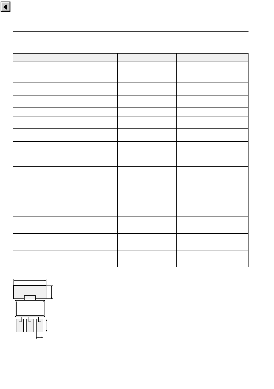
≠15
≠10
≠5
0
5
10
15
20
25
≠15≠10 ≠5 0
5
10 15 20 25 30 35 V
mA
V
DD
I
DD
T
A
= ≠40
∞
C
T
A
= 25
∞
C
T
A
= 170
∞
C
HAL 525, HAL 535
Fig. 3≠4: Typical supply current
versus supply voltage
0
0.5
1.0
1.5
2.0
2.5
3.0
3.5
4.0
4.5
5.0
1
2
3
4
5
6
7
8 V
mA
V
DD
I
DD
T
A
= ≠40
∞
C
T
A
= 25
∞
C
T
A
= 170
∞
C
T
A
= 100
∞
C
HAL 525, HAL 535
Fig. 3≠5: Typical supply current
versus supply voltage
0
1
2
3
4
5
≠50
0
50
100
150
200
∞
C
mA
T
A
I
DD
V
DD
= 3.8 V
V
DD
= 12 V
V
DD
= 24 V
HAL 525, HAL 535
Fig. 3≠6: Typical supply current
versus ambient temperature
0
20
40
60
80
100
120
140
160
≠50
0
50
100
150
200
∞
C
kHz
T
A
f
osc
V
DD
= 3.8 V
V
DD
= 4.5 V...24 V
HAL 525, HAL 535
Fig. 3≠7: Typ. internal chopper frequency
versus ambient temperature
HAL525, HAL535
Micronas
11
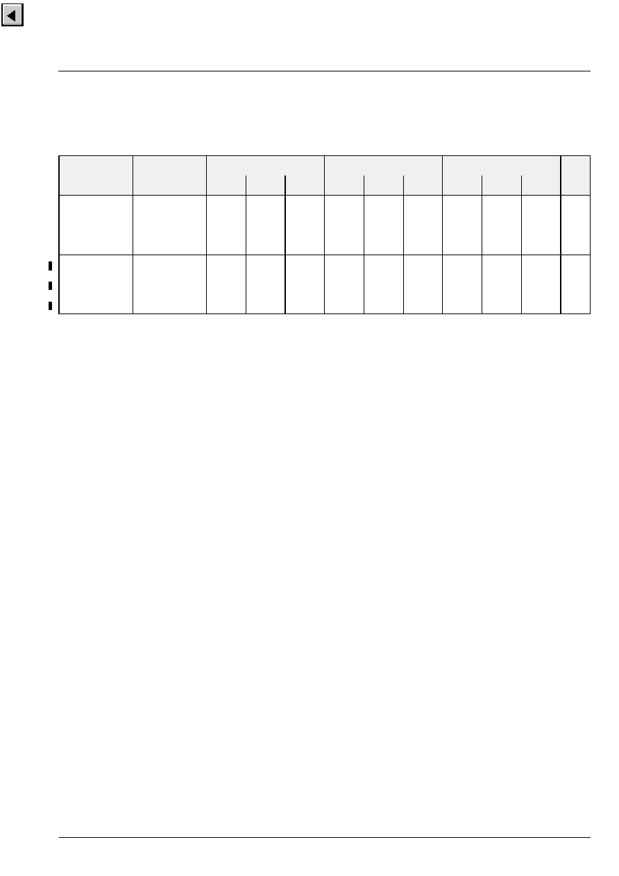
0
50
100
150
200
250
300
350
400
0
5
10
15
20
25
30 V
mV
V
DD
V
OL
T
A
= ≠40
∞
C
T
A
= 25
∞
C
T
A
= 170
∞
C
I
O
= 20 mA
T
A
= 100
∞
C
HAL 525, HAL 535
Fig. 3≠8: Typical output low voltage
versus supply voltage
0
100
200
300
400
500
600
3
4
5
6
7 V
mV
V
DD
V
OL
T
A
= ≠40
∞
C
T
A
= 25
∞
C
T
A
= 170
∞
C
I
O
= 20 mA
T
A
=100
∞
C
HAL 525, HAL 535
Fig. 3≠9: Typical output low voltage
versus supply voltage
0
100
200
300
400
≠50
0
50
100
150
200
∞
C
mV
T
A
V
OL
V
DD
= 3.8 V
V
DD
= 4.5 V
V
DD
= 24 V
I
O
= 20 mA
HAL 525, HAL 535
Fig. 3≠10: Typical output low voltage
versus ambient temperature
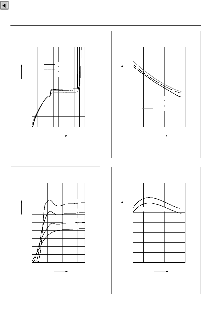
15
20
25
30
35 V
A
V
OH
I
OH
T
A
= ≠40
∞
C
T
A
= 170
∞
C
T
A
= 150
∞
C
T
A
= 100
∞
C
T
A
= 25
∞
C
10
≠6
10
≠5
10
≠4
10
≠3
10
≠2
10
≠1
10
0
10
1
10
2
10
3
10
4
HAL 525, HAL 535
Fig. 3≠11: Typ. output high current
versus output voltage
HAL525, HAL535
12
Micronas
≠50
0
50
100
150
200
∞
C
µ
A
T
A
I
OH
V
OH
= 24 V
V
OH
= 3.8 V
10
≠5
10
≠4
10
≠3
10
≠2
10
≠1
10
0
10
1
10
2
HAL 525, HAL 535
Fig. 3≠12: Typical output leakage current
versus ambient temperature
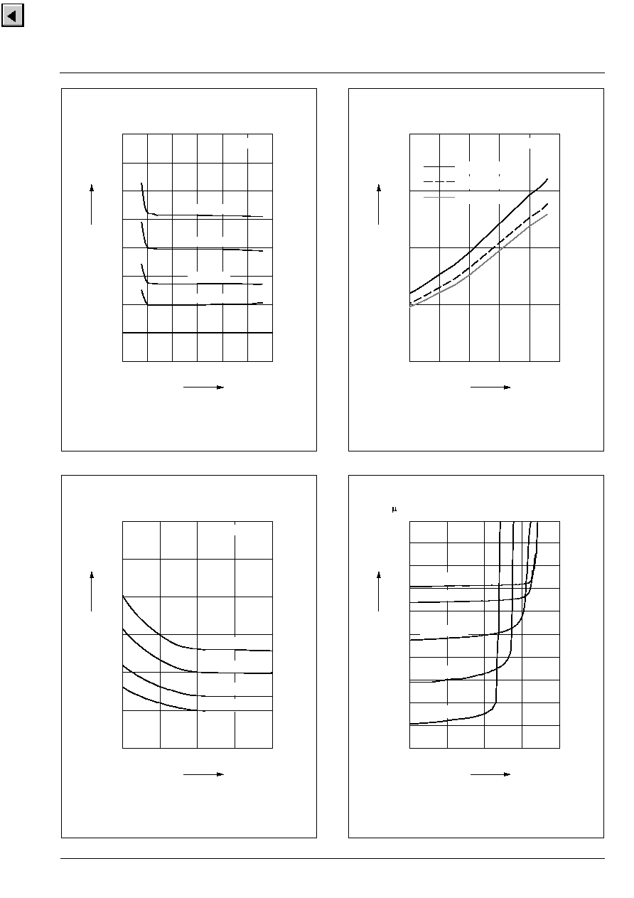
≠30
≠20
≠10
0
10
20
30
0.01
0.10
1.00
10.00 100.00 1000.00
dB
µ
A
f
I
DD
V
DD
= 12 V
T
A
= 25
∞
C
Quasi-Peak-
Measurement
max. spurious
signals
1
10
100
1000 MHz
HAL 525, HAL 535
Fig. 3≠13: Typ. spectrum of supply current
dB
µ
V
0
10
20
30
40
50
60
70
80
0.01
0.10
1.00
10.00 100.00 1000.00
1
10
100
1000 MHz
f
V
DD
V
P
= 12 V
T
A
= 25
∞
C
Quasi-Peak-
Measurement
test circuit
max. spurious
signals
HAL 525, HAL 535
Fig. 3≠14: Typ. spectrum of supply voltage

HAL525, HAL535
Micronas
13

HAL525
14
Micronas
4. Type Description
4.1. HAL525
The HAL 525 is a latching sensor (see Fig. 4≠1).
The output turns low with the magnetic south pole on
the branded side of the package and turns high with
the magnetic north pole on the branded side. The out-
put does not change if the magnetic field is removed.
For changing the output state, the opposite magnetic
field polarity must be applied.
For correct functioning in the application, the sensor
requires both magnetic polarities (north and south) on
the branded side of the package.
Magnetic Features:
≠ switching type: latching
≠ low sensitivity
≠ typical B
ON
: 14 mT at room temperature
≠ typical B
OFF
:
-
14 mT at room temperature
≠ operates with static magnetic fields and dynamic
magnetic fields up to 10 kHz
≠ typical temperature coefficient of magnetic switching
points is
-
2000 ppm/K
Applications
The HAL525 is the optimal sensor for applications with
alternating magnetic signals such as:
≠ multipole magnet applications,
≠ rotating speed measurement,
≠ commutation of brushless DC motors, and
≠ window lifter.
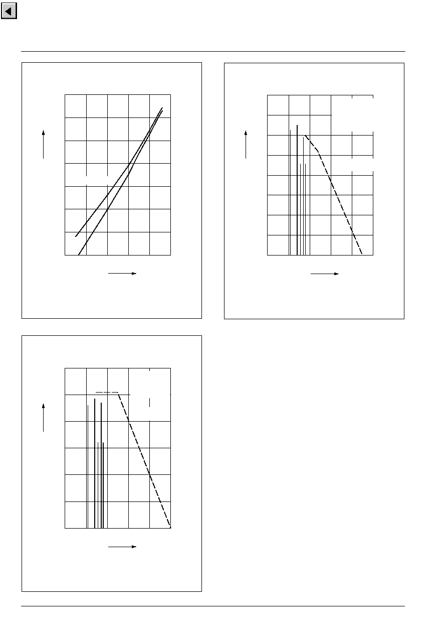
Fig. 4≠1: Definition of magnetic switching points for
the HAL525
Magnetic Characteristics at T
J
=
-
40
∞
C to +170
∞
C, V
DD
= 3.8 V to 24 V,
Typical Characteristics for V
DD
= 12 V
Magnetic flux density values of switching points.
Positive flux density values refer to the magnetic south pole at the branded side of the package.
The hysteresis is the difference between the switching points B
HYS
= B
ON
-
B
OFF
The magnetic offset is the mean value of the switching points B
OFFSET
= (B
ON
+ B
OFF
) / 2
B
OFF
B
ON
0
V
OL
V
O
Output Voltage
B
B
HYS
Parameter
On point B
ON
Off point B
OFF
Hysteresis B
HYS
Magnetic Offset
Unit
T
J
Min.
Typ.
Max.
Min.
Typ.
Max.
Min.
Typ.
Max.
Min.
Typ.
Max.
-
40
∞
C
11.8
15.8
19.2
-
19.2
-
15.8
-
11.8
27.4
31.6
35.8
0
mT
25
∞
C
11
14
17
-
17
-
14
-
11
24
28
32
-
2
0
2
mT
100
∞
C
8
11
15.5
-
15.5
-
11
-
8
18.5
22
28.7
0
mT
140
∞
C
6.5
10
14
-
14
-
10
-
6.5
16
20
26
0
mT
170
∞
C
5
8.5
13
-
13
-
8.5
-
5
12
17
25
0
mT
HAL525
Micronas
15
Note: In the diagram "Magnetic switching points ver-
sus ambient temperature" the curves for B
ON
min, B
ON-
max, B
OFF
min, and B
OFF
max refer to junction temper-
ature, whereas typical curves refer to ambient
temperature.
≠20
≠15
≠10
≠5
0
5
10
15
20
0
5
10
15
20
25
30 V
mT
V
DD
B
ON
B
OFF
HAL525
B
ON
B
OFF
T
A
= ≠40
∞
C
T
A
= 25
∞
C
T
A
= 170
∞
C
T
A
= 100
∞
C
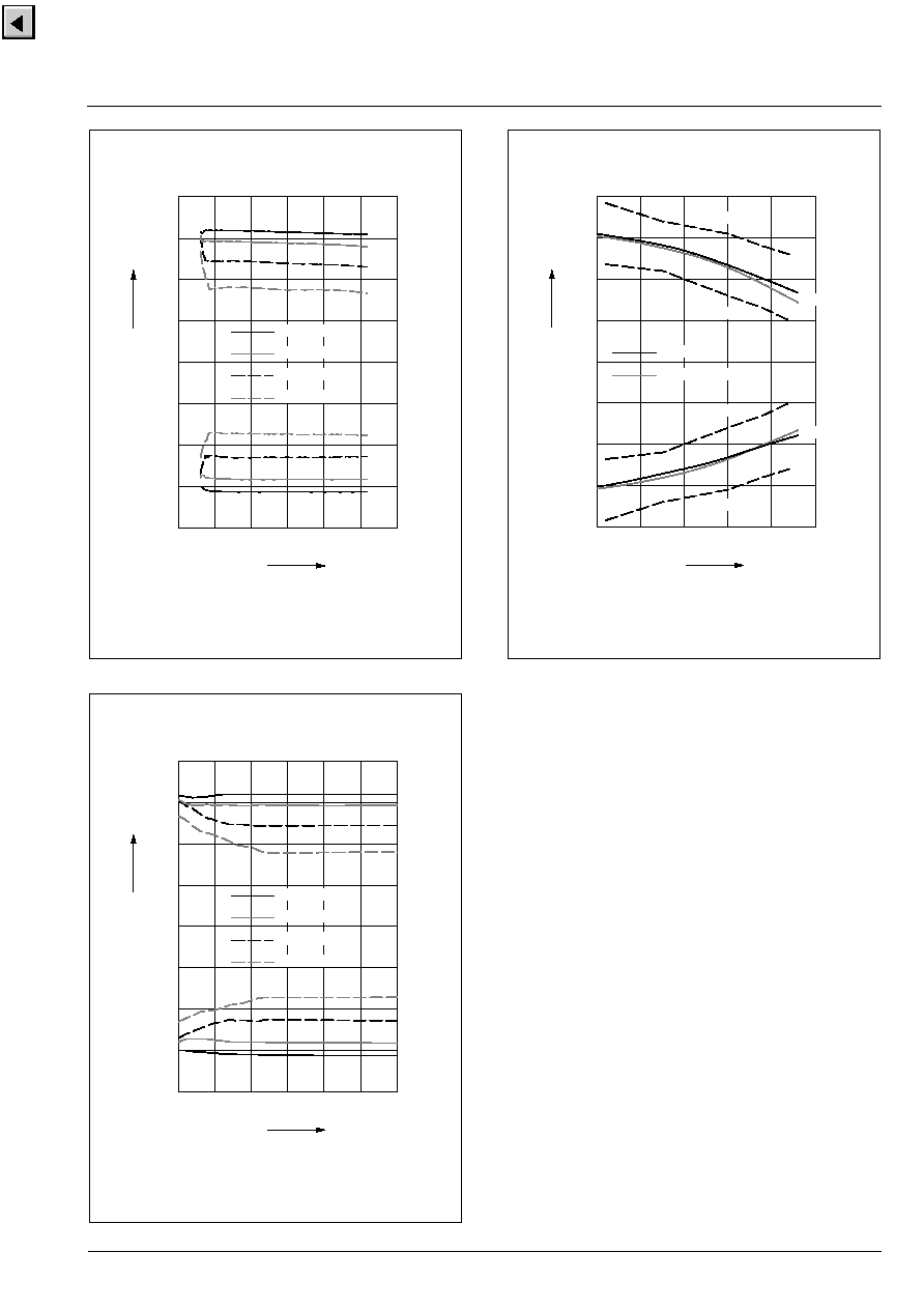
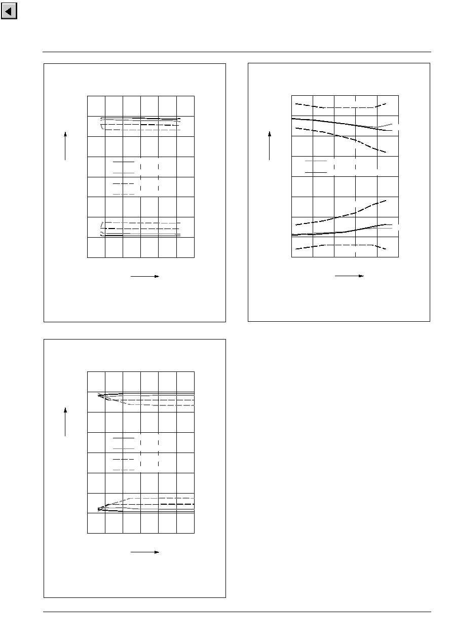
Fig. 4≠2: Typ. magnetic switching points
versus supply voltage
≠20
≠15
≠10
≠5
0
5
10
15
20
3
3.5
4.0
4.5
5.0
5.5
6.0 V
mT
V
DD
B
ON
B
OFF
B
ON
B
OFF
T
A
= ≠40
∞
C
T
A
= 25
∞
C
T
A
= 170
∞
C
T
A
= 100
∞
C
HAL525
Fig. 4≠3: Typ. magnetic switching points
versus supply voltage
≠20
≠15
≠10
≠5
0
5
10
15
20
≠50
0
50
100
150
200
∞
C
mT
T
A
, T
J
B
ON
B
OFF
B
ON
max
B
ON
min
B
OFF
max
B
OFF
min
V
DD
= 4.5 V...24 V
V
DD
= 3.8 V
B
ON
typ
B
OFF
typ
HAL525
Fig. 4≠4: Magnetic switching points
versus temperature
HAL535
16
Micronas
4.2. HAL535
The HAL 535 is a latching sensor (see Fig. 4≠5).
The output turns low with the magnetic south pole on
the branded side of the package and turns high with
the magnetic north pole on the branded side. The out-
put does not change if the magnetic field is removed.
For changing the output state, the opposite magnetic
field polarity must be applied.
For correct functioning in the application, the sensor
requires both magnetic polarities (north and south) on
the branded side of the package.
Magnetic Features:
≠ switching type: latching
≠ low sensitivity
≠ typical B
ON
: 13.5 mT at room temperature
≠ typical B
OFF
:
-
13.5 mT at room temperature
≠ operates with static magnetic fields and dynamic
magnetic fields up to 10 kHz
≠ typical temperature coefficient of magnetic switching
points is
-
1000 ppm/K
Applications
The HAL535 is the optimal sensor for applications with
alternating magnetic signals such as:
≠ multipole magnet applications,
≠ rotating speed measurement,
≠ commutation of brushless DC motors, and
≠ window lifter.
Fig. 4≠5: Definition of magnetic switching points for
the HAL535
Magnetic Characteristics at T
J
=
-
40
∞
C to +170
∞
C, V
DD
= 3.8 V to 24 V,
Typical Characteristics for V
DD
= 12 V
Magnetic flux density values of switching points.
Positive flux density values refer to the magnetic south pole at the branded side of the package.
The hysteresis is the difference between the switching points B
HYS
= B
ON
-
B
OFF
The magnetic offset is the mean value of the switching points B
OFFSET
= (B
ON
+ B
OFF
) / 2
B
OFF
B
ON
0
V
OL
V
O
Output Voltage
B
B
HYS
Parameter
On point B
ON
Off point B
OFF
Hysteresis B
HYS
Magnetic Offset
Unit
T
J
Min.
Typ.
Max.
Min.
Typ.
Max.
Min.
Typ.
Max.
Min.
Typ.
Max.
-
40
∞
C
12
15
18
-
18
-
15
-
12
25
30
35
0
mT
25
∞
C
11
13.8
17
-
17
-
13.8
-
11
23
27.6
32
0
mT
100
∞
C
9
13
17
-
17
-
13
-
9
20
26
31.5
0
mT
140
∞
C
7
12.5
17
-
17
-
12.5
-
7
18
25
31
0
mT
170
∞
C
6
12
18
-
18
-
12
-
6
17
24
31
0
mT
HAL535
Micronas
17
Note: In the diagram "Magnetic switching points ver-
sus ambient temperature" the curves for B
ON
min, B
ON-
max, B
OFF
min, and B
OFF
max refer to junction temper-
ature, whereas typical curves refer to ambient
temperature.
≠20
≠15
≠10
≠5
0
5
10
15
20
0
5
10
15
20
25
30 V
mT
V
DD
B
ON
B
OFF
HAL 535
B
ON
B
OFF
T
A
= ≠40
∞
C
T
A
= 25
∞
C
T
A
= 170
∞
C
T
A
= 100
∞
C
Fig. 4≠6: Typ. magnetic switching points
versus supply voltage
≠20
≠15
≠10
≠5
0
5
10
15
20
3
3.5
4.0
4.5
5.0
5.5
6.0 V
mT
V
DD
B
ON
B
OFF
HAL 535
B
ON
B
OFF
T
A
= ≠40
∞
C
T
A
= 25
∞
C
T
A
= 170
∞
C
T
A
= 100
∞
C
Fig. 4≠7: Typ. magnetic switching points
versus supply voltage
≠20
≠15
≠10
≠5
0
5
10
15
20
≠50
0
50
100
150
200
HAL 535
∞
C
mT
T
A
, T
J
B
ON
B
OFF
B
ON
max
B
ON
min
B
OFF
max
B
OFF
min
V
DD
= 3.8 V
V
DD
= 4.5 V... 24 V
B
OFF
typ
B
ON
typ
Fig. 4≠8: Magnetic switching points
versus temperature
HAL525, HAL535
18
Micronas
5. Application Notes
5.1. Ambient Temperature
Due to the internal power dissipation, the temperature
on the silicon chip (junction temperature T
J
) is higher
than the temperature outside the package (ambient
temperature T
A
).
T
J
= T
A
+
T
At static conditions, the following equation is valid:
T = I
DD
* V
DD
* R
th
For typical values, use the typical parameters. For
worst case calculation, use the max. parameters for
I
DD
and R
th
, and the max. value for V
DD
from the appli-
cation.
For all sensors, the junction temperature range T
J
is
specified. The maximum ambient temperature T
Amax
can be calculated as:
T
Amax
= T
Jmax
-
T
5.2. Extended Operating Conditions
All sensors fulfill the electrical and magnetic character-
istics when operated within the Recommended Oper-
ating Conditions (see page 7).
Supply Voltage Below 3.8 V
Typically, the sensors operate with supply voltages
above 3 V, however, below 3.8 V some characteristics
may be outside the specification.
Note: The functionality of the sensor below 3.8 V is not
tested. For special test conditions, please contact Mic-
ronas.
5.3. Start-up Behavior
Due to the active offset compensation, the sensors
have an initialization time (enable time t
en(O)
) after
applying the supply voltage. The parameter t
en(O)
is
specified in the Electrical Characteristics (see page 8).
During the initialization time, the output state is not
defined and the output can toggle. After t
en(O)
, the out-
put will be low if the applied magnetic field B is above
B
ON
. The output will be high if B is below B
OFF
.
For magnetic fields between B
OFF
and B
ON
, the output
state of the HAL sensor after applying V
DD
will be
either low or high. In order to achieve a well-defined
output state, the applied magnetic field must be above
B
ONmax
, respectively, below B
OFFmin
.
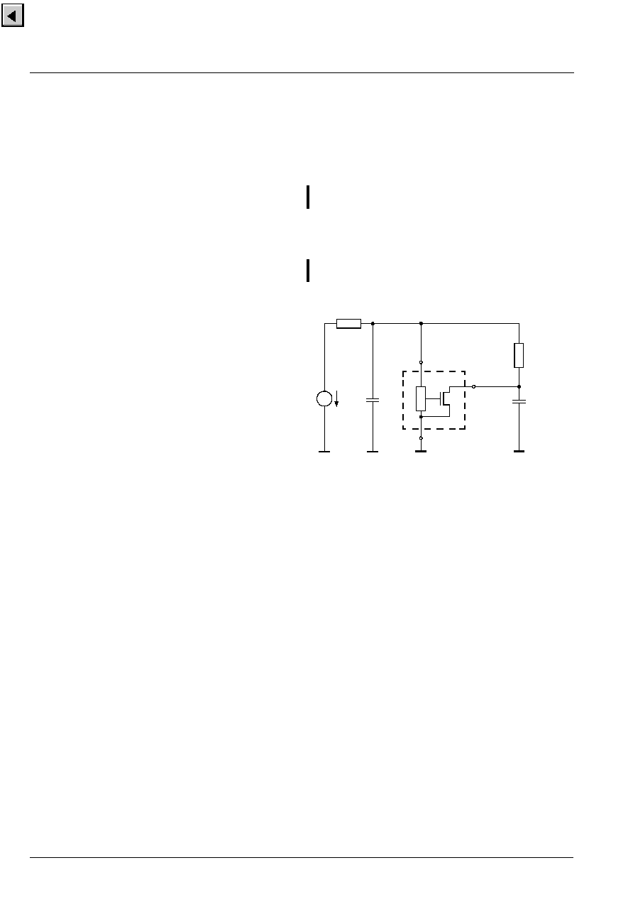
5.4. EMC and ESD
For applications with disturbances on the supply line or
radiated disturbances, a series resistor and a capacitor
are recommended (see Fig. 5≠1). The series resistor
and the capacitor should be placed as closely as pos-
sible to the HAL sensor.
Applications with this arrangement passed the EMC
tests according to the product standards DIN 40839).
Note: The international standard ISO 7637 is similar to
the used product standard DIN 40839.
Please contact Micronas for the detailed investigation
reports with the EMC and ESD results.
Fig. 5≠1: Test circuit for EMC investigations
R
V
220
V
EMC
V
P
4.7 nF
V
DD
OUT
GND
1
2
3
R
L
1.2 k
20 pF

HAL525, HAL535
Micronas
19

All information and data contained in this data sheet are without any
commitment, are not to be considered as an offer for conclusion of a
contract, nor shall they be construed as to create any liability. Any new
issue of this data sheet invalidates previous issues. Product availability
and delivery are exclusively subject to our respective order confirmation
form; the same applies to orders based on development samples deliv-
ered. By this publication, Micronas GmbH does not assume responsibil-
ity for patent infringements or other rights of third parties which may
result from its use.
Further, Micronas GmbH reserves the right to revise this publication and
to make changes to its content, at any time, without obligation to notify
any person or entity of such revisions or changes.
No part of this publication may be reproduced, photocopied, stored on a
retrieval system, or transmitted without the express written consent of
Micronas GmbH.
HAL525, HAL535
20
Micronas
Micronas GmbH
Hans-Bunte-Strasse 19
D-79108 Freiburg (Germany)
P.O. Box 840
D-79008 Freiburg (Germany)
Tel. +49-761-517-0
Fax +49-761-517-2174
E-mail: docservice@micronas.com
Internet: www.micronas.com
Printed in Germany
Order No. 6251-465-3DS
6. Data Sheet History
1. Final data sheet: "HAL525 Hall Effect Sensor IC",
April 23, 1997, 6251-465-1DS. First release of the final
data sheet.
2. Final data sheet: "HAL525 Hall Effect Sensor IC",
March 10, 1999, 6251-465-2DS. Second release of the
final data sheet. Major changes:
≠ additional package SOT-89B
≠ outline dimensions for SOT-89A and TO-92UA
changed
≠ electrical characteristics changed
≠ section 4.2.: Extended Operating Conditions added
≠ section 4.3.: Start-up Behavior added
3. Final data sheet: "HAL525, HAL535 Hall Effect
Sensor Family", Aug. 30, 2000, 6251-465-3DS. Third
release of the final data sheet. Major changes:
≠ new sensor HAL 535 added
≠ outline dimensions for SOT-89B: reduced toler-
ances
≠ SMD package SOT-89A removed
≠ temperature range "C" removed

Micronas
page 1 of 1
Subject:
Data Sheet Concerned:
Supplement:
Edition:
Data Sheet Supplement
Changes:
≠ position tolerance of the sensitive area reduced
≠ tolerances of the outline dimensions reduced
≠ thickness of the leadframe changed to 0.15 mm (old 0.125 mm)
≠ SOT-89A will be discontinued in December 2000
Position of sensitive area
Note: A mechanical tolerance of
±
0.05 mm applies to all dimensions where no tolerance is explicitly given.
Position tolerance of the sensitive area is defined in the package diagram.
HAL 114, 115
HAL 50x, 51x
HAL 621, 629
HAL 55x, HAL 56x
x
center of the package
center of the package
y
0.95 mm nominal
0.85
mm nominal
min.
0.25
2.55
0.4
0.4
0.4
1.5
3.0
0.06
±
0.04
branded side
SPGS0022-5-A3/2E
y
1
2
3
4
±
0.2
0.15
0.3
4.55
1.7
2
0.2
sensitive area
top view
1.15
Improvement of SOT-89B Package
HAL 114, 115, 6251-456-2DS, Dec. 20, 1999
HAL 50x, 51x, 6251-485-1DS, Feb. 16, 1999
HAL 55x, 56x, 6251-425-1DS, April 6, 1999
HAL 621, 629, 6251-504-1DS, Feb. 3, 2000
No. 1/ 6251-531-1DSS
July 4, 2000
HAL 11x, HAL 5xx, HAL 62x