 | –≠–ª–µ–∫—Ç—Ä–æ–Ω–Ω—ã–π –∫–æ–º–ø–æ–Ω–µ–Ω—Ç: HAL584 | –°–∫–∞—á–∞—Ç—å:  PDF PDF  ZIP ZIP |
HAL571, 573...575,
HAL581, 584
Two-Wire Hall Effect
Sensor Family
Edition Oct. 11, 2000
6251-538-1AI
ADVANCE INFORMATION
MICRONAS
MICRONAS

HAL57x, HAL58x
ADVANCE INFORMATION
2
Micronas
Contents
Page
Section
Title
3
1.
Introduction
3
1.1.
Features
3
1.2.
Family Overview
4
1.3.
Marking Code
4
1.4.
Operating Junction Temperature Range
4
1.5.
Hall Sensor Package Codes
4
1.6.
Solderability
5
2.
Functional Description
6
3.
Specifications
6
3.1.
Outline Dimensions
6
3.2.
Dimensions of Sensitive Area
6
3.3.
Positions of Sensitive Areas
7
3.4.
Absolute Maximum Ratings
7
3.5.
Recommended Operating Conditions
8
3.6.
Electrical Characteristics
9
3.7.
Magnetic Characteristics Overview
12
4.
Type Descriptions
12
4.1.
HAL 571
13
4.2.
HAL 573
14
4.3.
HAL 574
15
4.4.
HAL 575
16
4.5.
HAL 581
17
4.6.
HAL 584
18
5.
Application Notes
18
5.1.
Application Circuit
18
5.2.
Extended Operating Conditions
18
5.3.
Start-up Behavior
19
5.4.
Ambient Temperature
19
5.5.
EMC and ESD
20
6.
Data Sheet History
HAL57x, HAL58x
ADVANCE INFORMATION
3
Micronas
Two-Wire Hall Effect Sensor Family
in CMOS technology
1. Introduction
This sensor family consists of different two-wire Hall
switches produced in CMOS technology. All sensors
change the current consumption depending on the ex-
ternal magnetic field and require only two wires between
sensor and evaluation circuit. The sensors of this family
differ in the magnetic switching behavior and switching
points.
The sensors include a temperature-compensated Hall
plate with active offset compensation, a comparator, and
a current source. The comparator compares the actual
magnetic flux through the Hall plate (Hall voltage) with
the fixed reference values (switching points). According-
ly, the current source is switched on (high current
consumption) or off (low current consumption).
The active offset compensation leads
to constant mag-
netic characteristics in the full
supply voltage and tem-
perature range. In addition, the magnetic parameters
are robust against mechanical stress effects.
The sensors are designed for industrial and automotive
applications and operate with supply voltages from 3.75
V to 24 V in the junction temperature range from ≠40
∞
C
up to 140
∞
C. All sensors are available in the SMD-pack-
age SOT-89B and in the leaded version TO-92UA.
1.1. Features:
≠ current output for two-wire applications
≠ low current consumption: 5 mA ... 6.9 mA
≠ high current consumption: 12 mA ... 17 mA
≠ junction temperature range from ≠40
∞
C up to 140
∞
C.
≠ operates from 3.75 V to 24 V supply voltage
≠ operates with static magnetic fields and dynamic mag-
netic fields up to 10 kHz
≠ switching offset compensation at typically 145 kHz
≠ overvoltage and reverse-voltage protection
≠ magnetic characteristics are robust against mechani-
cal stress effects
≠ constant magnetic switching points over a wide supply
voltage range
≠ the decrease of magnetic flux density caused by rising
temperature in the sensor system is compensated by
a built-in negative temperature coefficient of the mag-
netic characteristics
≠ ideal sensor for applications in extreme automotive
and industrial environments
≠ EMC corresponding to DIN 40839
1.2. Family Overview
Type
Switching
Behavior
Sensitivity
see
Page
571
unipolar
medium
12
573
unipolar
low
13
574
unipolar
medium
14
575
latching
medium
15
581
unipolar
inverted
medium
16
584
unipolar
inverted
medium
17
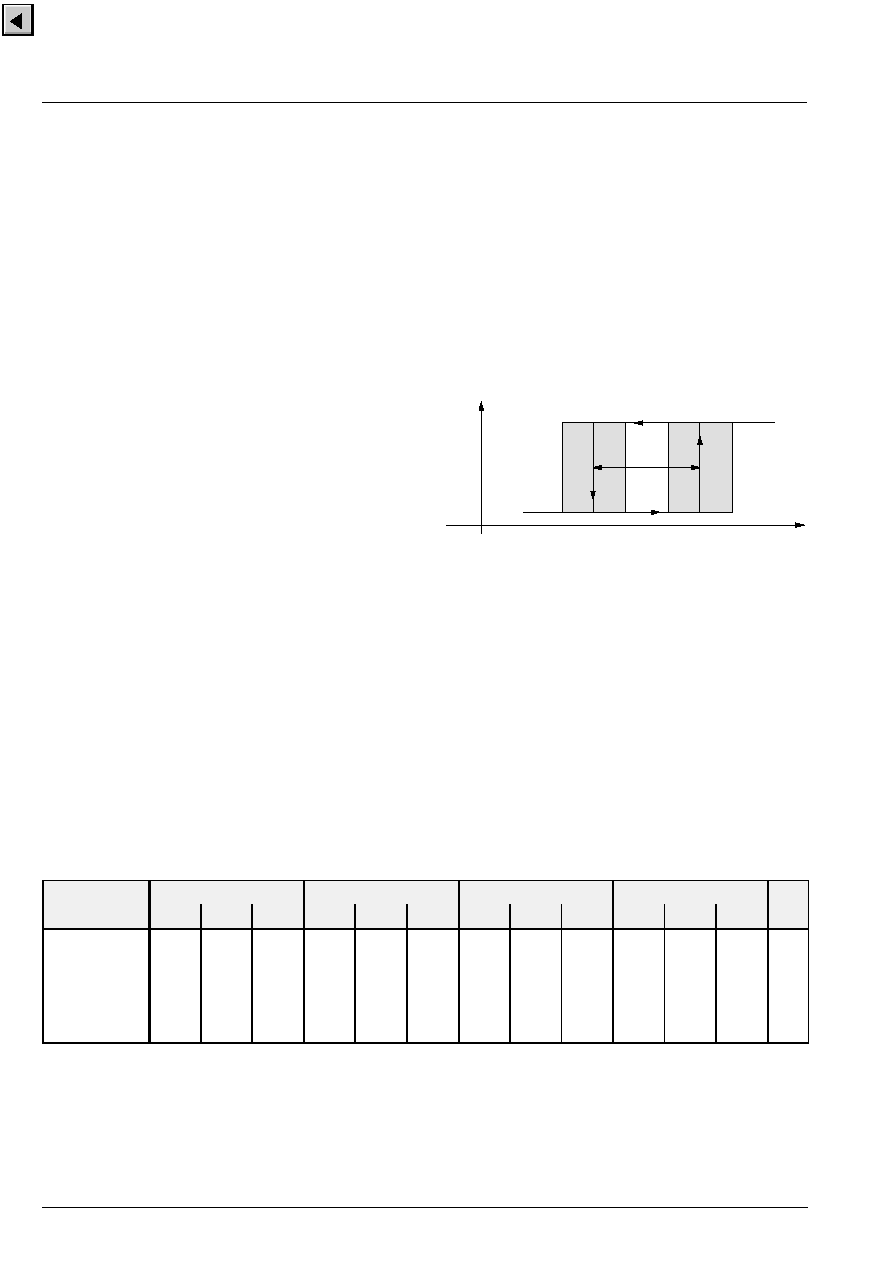
Unipolar Switching Sensors:
The sensor turns to high current consumption with the
magnetic south pole on the branded side of the package
and turns to low consumption if the magnetic field is
removed. The sensor does not respond to the magnetic
north pole on the branded side.
B
HYS
Current consumption
0
B
ON
B
OFF
I
DDlow
B
Fig. 1≠1: Unipolar Switching Sensor
I
DDhigh
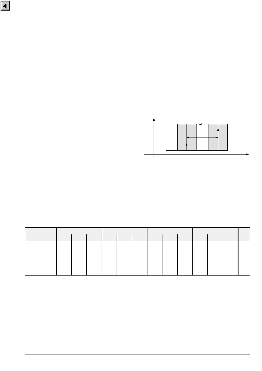
Unipolar Inverted Switching Sensors:
The sensor turns to low current consumption with the
magnetic south pole on the branded side of the package
and turns to high consumption if the magnetic field is
removed. The sensor does not respond to the magnetic
north pole on the branded side.
B
HYS
0
B
OFF
B
ON
B
Fig. 1≠2: Unipolar Inverted Switching Sensor
I
DDhigh
I
DDlow
Current consumption
HAL57x, HAL58x
ADVANCE INFORMATION
4
Micronas
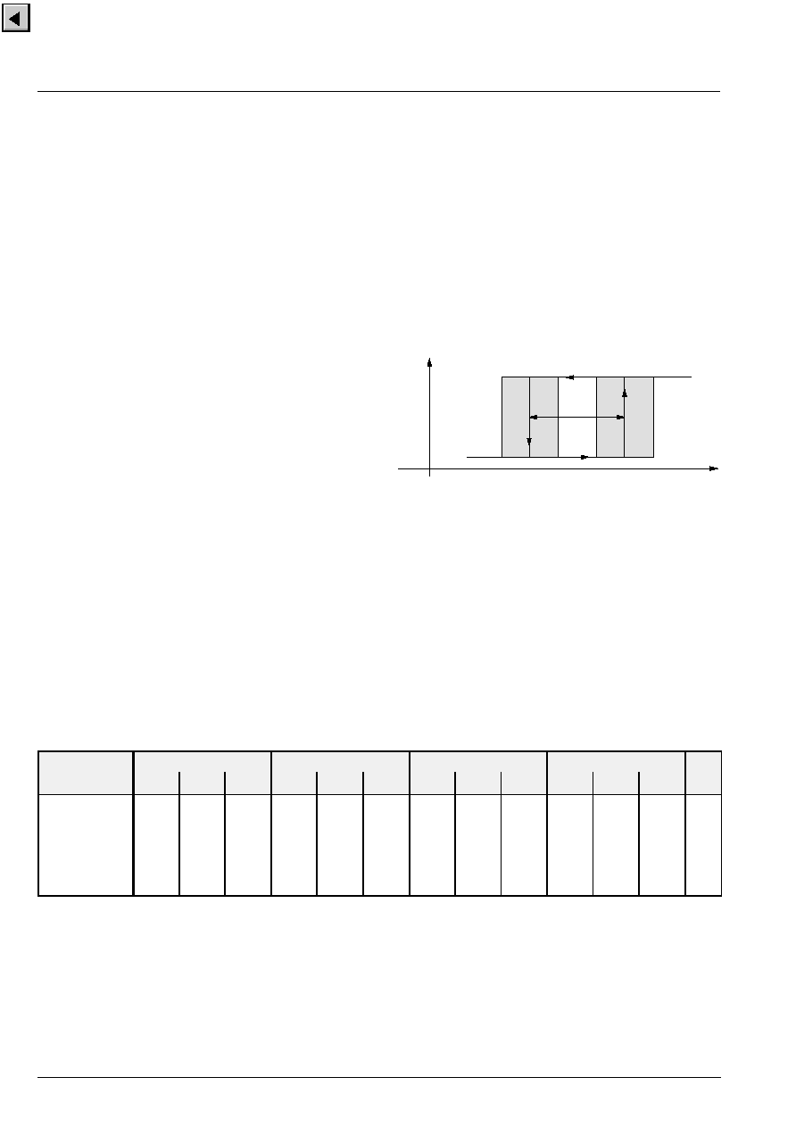
Latching Sensors:
The sensor turns to high current consumption with the
magnetic south pole on the branded side of the package
and turns to low consumption with the magnetic north
pole on the branded side. The current consumption does
not change if the magnetic field is removed. For chang-
ing the current consumption, the opposite magnetic field
polarity must be applied.
B
HYS
Current consumption
0
B
ON
B
OFF
I
DDlow
B
Fig. 1≠3: Latching Sensor
I
DDhigh
1.3. Marking Code
All Hall sensors have a marking on the package surface
(branded side). This marking includes the name of the
sensor and the temperature range.
Type
Temperature Range
K
E
HAL571
571K
571E
HAL573
573K
573E
HAL574
574K
574E
HAL575
575K
575E
HAL581
581K
581E
HAL584
584K
584E
1.4. Operating Junction Temperature Range
The Hall sensors from Micronas are specified to the chip
temperature (junction temperature T
J
).
K: T
J
= ≠40
∞
C to +140
∞
C
E: T
J
= ≠40
∞
C to +100
∞
C
Note: Due to the high power dissipation at high current
consumption, there is a difference between the ambient
temperature (T
A
) and junction temperature. Please refer
section 5.4. on page 19 for details.
1.5. Hall Sensor Package Codes
Type: 57x or 58x
HAL XXXPA-T
Temperature Range: K or E
Package: SF for SOT-89B
UA for TO-92UA
Type: 581
Package: TO-92UA
Temperature Range: T
J
= ≠40
∞
C to +100
∞
C
Example: HAL 581UA-E
Hall sensors are available in a wide variety of packaging
versions and quantities. For more detailed information,
please refer to the brochure: "Ordering Codes for Hall
Sensors".
1.6. Solderability
all packages: according to IEC68-2-58
During soldering reflow processing and manual rework-
ing, a component body temperature of 260
∞
C should not
be exceeded.
Components stored in the original packaging should
provide a shelf life of at least 12 months, starting from the
date code printed on the labels, even in environments as
extreme as 40
∞
C and 90% relative humidity.
Fig. 1≠4: Pin configuration
GND
2
1
V
DD
3
HAL57x, HAL58x
ADVANCE INFORMATION
5
Micronas
2. Functional Description
The HAL 57x, HAL 58x two-wire sensors are monolithic
integrated circuits which switch in response to magnetic
fields. If a magnetic field with flux lines perpendicular to
the sensitive area is applied to the sensor, the biased
Hall plate forces a Hall voltage proportional to this field.
The Hall voltage is compared with the actual threshold
level in the comparator. The temperature-dependent
bias increases the supply voltage of the Hall plates and
adjusts the switching points to the decreasing induction
of magnets at higher temperatures.
If the magnetic field exceeds the threshold levels, the
current source switches to the corresponding state. In
the low current consumption state, the current source is
switched off and the current consumption is caused only
by the current through the Hall sensor. In the high current
consumption state, the current source is switched on
and the current consumption is caused by the current
through the Hall sensor and the current source. The
built-in hysteresis eliminates oscillation and provides
switching behavior of the output signal without bounc-
ing.
Magnetic offset caused by mechanical stress is com-
pensated for by using the "switching offset compensa-
tion technique". An internal oscillator provides a two-
phase clock. In each phase, the current is forced through
the Hall plate in a different direction, and the Hall voltage
is measured. At the end of the two phases, the Hall volt-
ages are averaged and thereby the offset voltages are
eliminated. The average value is compared with the
fixed switching points. Subsequently, the current con-
sumption switches to the corresponding state. The
amount of time elapsed from crossing the magnetic
switching level to switching of the current level can vary
between zero and 1/f
osc
.
Shunt protection devices clamp voltage peaks at the
V
DD
-pin together with external series resistors. Reverse
current is limited at the V
DD
-pin by an internal series
resistor up to ≠15 V. No external protection diode is
needed for reverse voltages ranging from 0 V to ≠15 V.
Fig. 2≠1: HAL 57x, HAL 58x block diagram
Temperature
Dependent
Bias
Switch
Hysteresis
Control
Comparator
Current
Source
V
DD
1
Clock
Hall Plate
GND
2, 3
HAL 57x, HAL58x
Reverse
Voltage &
Overvoltage
Protection
t
I
DDlow
I
DD
1/f
osc
= 6.9
µ
s
I
DDhigh
B
B
OFF
f
osc
t
t
t
I
DD
t
B
ON
Fig. 2≠2: Timing diagram (example: HAL 581)
HAL57x, HAL58x
ADVANCE INFORMATION
6
Micronas
3. Specifications
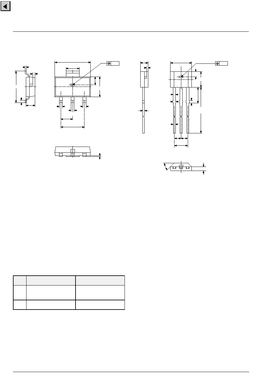
3.1. Outline Dimensions
Fig. 3≠1:
Plastic Small Outline Transistor Package
(SOT-89B)
Weight approximately 0.035 g
Dimensions in mm
4.55
1.7
min.
0.25
2.55
0.4
0.4
0.4
1.5
3.0
0.06
±
0.04
branded side
SPGS0022-5-A3/2E
y
1
2
3
4
±
0.2
0.15
0.3
2
0.2
sensitive area
top view
1.15
3.2. Dimensions of Sensitive Area
0.25 mm x 0.12 mm
3.3. Positions of Sensitive Areas
SOT-89B
TO-92UA
x
center of
the package
center of
the package
y
0.85 mm nominal
0.9 mm nominal
Fig. 3≠2:
Plastic Transistor Single Outline Package
(TO-92UA)
Weight approximately 0.12 g
Dimensions in mm
0.75
±
0.2
3.1
±
0.2
0.55
branded side
0.36
0.8
0.3
45
∞
y
14.0
min.
1.27
1.27
2.54
1
2
3
0.42
4.06
±
0.1
3.05
±
0.1
0.48
SPGS7002-9-A/2E
0.4
sensitive area
1.5
Note: For all package diagrams, a mechanical tolerance
of
±
0.05 mm applies to all dimensions where no tolerance
is explicitly given.
The improvement of the TO-92UA package with the re-
duced tolerances will be introduced end of 2001.
HAL57x, HAL58x
ADVANCE INFORMATION
7
Micronas
3.4. Absolute Maximum Ratings
Symbol
Parameter
Pin No.
Min.
Max.
Unit
V
DD
Supply Voltage
1
≠15
1) 2)
28
2)
V
I
DDZ
Supply Current through
Protection Device
1
≠50
2)
≠200
3)
50
2)
200
3)
mA
mA
T
S
Storage Temperature Range
≠65
150
∞
C
T
J
Junction Temperature Range
≠40
150
∞
C
1)
≠18 V with a 100
series resistor at pin 1 (≠16 V with a 30
series resistor)
2)
as long as T
J
max
is not exceeded
2)
with a 220
series resistance at pin 1 corresponding to test circuit 1 (see Fig. 5≠3)
3)
t < 2 ms
Stresses beyond those listed in the "Absolute Maximum Ratings" may cause permanent damage to the device. This
is a stress rating only. Functional operation of the device at these or any other conditions beyond those indicated in the
"Recommended Operating Conditions/Characteristics" of this specification is not implied. Exposure to absolute maxi-
mum ratings conditions for extended periods may affect device reliability.
3.5. Recommended Operating Conditions
Symbol
Parameter
Pin No.
Min.
Max.
Unit
V
DD
Supply Voltage
1
3.75
24
V
T
A
Ambient Temperature for Continuous
Operation
≠40
85
1)
∞
C
t
on
Supply Time for Pulsed Mode
30
≠
µ
s
1)
when using the the "K" type and V
DD
16 V
Note: Due to the high power dissipation at high current consumption, there is a difference between the ambient temper-
ature (T
A
) and junction temperature. The power dissipation can be reduced by repeatedly switching the supply voltage
on and off (pulse mode). Please refer to section 5.4. on page 19 for details.
HAL57x, HAL58x
ADVANCE INFORMATION
8
Micronas
3.6. Electrical Characteristics at T
J
= ≠40
∞
C to +140
∞
C , V
DD
= 3.75 V to 24 V, as not otherwise specified in Conditions
Typical Characteristics for T
J
= 25
∞
C and V
DD
= 12 V
Symbol
Parameter
Pin No.
Min.
Typ.
Max.
Unit
Conditions
I
DDlow
Low Current Consumption
over Temperature Range
1
5
6
6.9
mA
I
DDhigh
High Current Consumption
over Temperature Range
1
12
14.3
17
mA
V
DDZ
Overvoltage Protection
at Supply
1
≠
28.5
32
V
I
DD
= 25 mA,
T
J
= 25
∞
C,
t = 20 ms
f
osc
Internal Oscillator
Chopper Frequency
≠
90
145
≠
kHz
T
J
= 25
∞
C
f
osc
Internal Oscillator Chopper Fre-
quency over Temperature Range
≠
75
145
≠
kHz
t
en(O)
Enable Time of Output after
Setting of V
DD
1
20
30
µ
s
1)
t
r
Output Rise Time
1
0.4
1.6
µ
s
V
DD
= 12 V, R
s
= 30
t
f
Output Fall Time
1
0.4
1.6
µ
s
V
DD
= 12 V, R
s
= 30
R
thJSB
case
SOT-89B
Thermal Resistance Junction
to Substrate Backside
≠
≠
150
200
K/W
Fiberglass Substrate
30 mm x 10 mm x 1.5mm,
pad size see Fig. 3≠3
R
thJA
case
TO-92UA
Thermal Resistance Junction
to Soldering Point
≠
≠
150
200
K/W
1)
B > B
ON
+ 2 mT or B < B
OFF
≠ 2 mT for HAL 57x, B > B
OFF
+ 2 mT or B < B
ON
≠ 2 mT for HAL 58x
Fig. 3≠3: Recommended pad size SOT-89B
Dimensions in mm
5.0
2.0
2.0
1.0

HAL57x, HAL58x
ADVANCE INFORMATION
9
Micronas
3.7. Magnetic Characteristics Overview at T
J
= ≠40
∞
C to +140
∞
C, V
DD
= 3.75 V to 24 V,
Typical Characteristics for V
DD
= 12 V
Magnetic flux density values of switching points.
Positive flux density values refer to the magnetic south pole at the branded side of the package.
Sensor
Parameter
On point B
ON
Off point B
OFF
Hysteresis B
HYS
Unit
Switching Type
T
J
Min.
Typ.
Max.
Min.
Typ.
Max.
Min.
Typ.
Max.
HAL 571
≠40
∞
C
8
12
15.5
6.5
10
13.8
0.5
2
3
mT
unipolar
25
∞
C
8
12
15.5
6.5
10
13.8
0.5
2
3
mT
100
∞
C
8
12
15.5
6.5
10
13.8
0.5
2
3
mT
140
∞
C
tbd
≠
tbd
tbd
≠
tbd
tbd
≠
tbd
mT
HAL 573
≠40
∞
C
40.2
45.7
51.2
38.2
43.7
49.2
0.5
2
4
mT
unipolar
25
∞
C
38
43.5
49
36
41.5
47
0.5
2
4
mT
100
∞
C
34
40
46
32
38
44
0.5
2
4
mT
140
∞
C
tbd
≠
tbd
tbd
≠
tbd
tbd
≠
tbd
mT
HAL 574
≠40
∞
C
5.5
9.2
12
5
7.2
11.5
0.5
2
3
mT
unipolar
25
∞
C
5.5
9.2
12
5
7.2
11.5
0.5
2
3
mT
100
∞
C
5.5
9.2
12
5
7.2
11.5
0.5
2
3
mT
140
∞
C
tbd
≠
tbd
tbd
≠
tbd
tbd
≠
tbd
mT
HAL 575
≠40
∞
C
0.5
4
8
≠8
≠4
≠0.5
5
8
11
mT
latching
25
∞
C
0.5
4
8
≠8
≠4
≠0.5
5
8
11
mT
100
∞
C
0.5
4
8
≠8
≠4
≠0.5
5
8
11
mT
140
∞
C
tbd
≠
tbd
tbd
≠
tbd
tbd
≠
tbd
mT
HAL 581
≠40
∞
C
6.5
10
13.8
8
12
15.5
0.5
2
3
mT
unipolar
25
∞
C
6.5
10
13.8
8
12
15.5
0.5
2
3
mT
inverted
100
∞
C
6.5
10
13.8
8
12
15.5
0.5
2
3
mT
140
∞
C
tbd
≠
tbd
tbd
≠
tbd
tbd
≠
tbd
mT
HAL 584
≠40
∞
C
5
7.2
11.5
5.5
9.2
12
0.5
2
3
mT
unipolar
25
∞
C
5
7.2
11.5
5.5
9.2
12
0.5
2
3
mT
inverted
100
∞
C
5
7.2
11.5
5.5
9.2
12
0.5
2
3
mT
140
∞
C
tbd
≠
tbd
tbd
≠
tbd
tbd
≠
tbd
mT
Note: For detailed descriptions of the individual types, see pages 12 and following.
HAL57x, HAL58x
ADVANCE INFORMATION
10
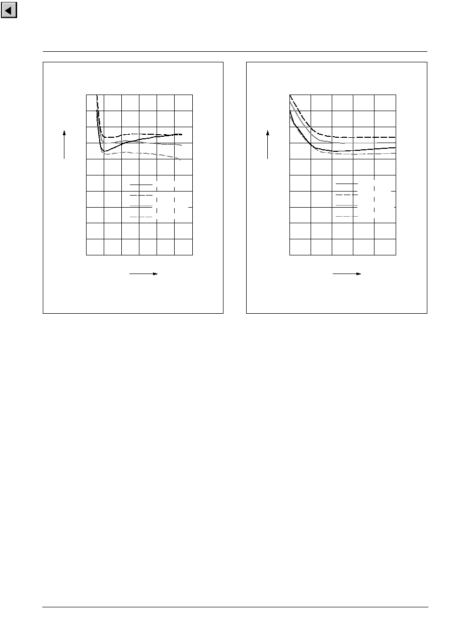
Micronas
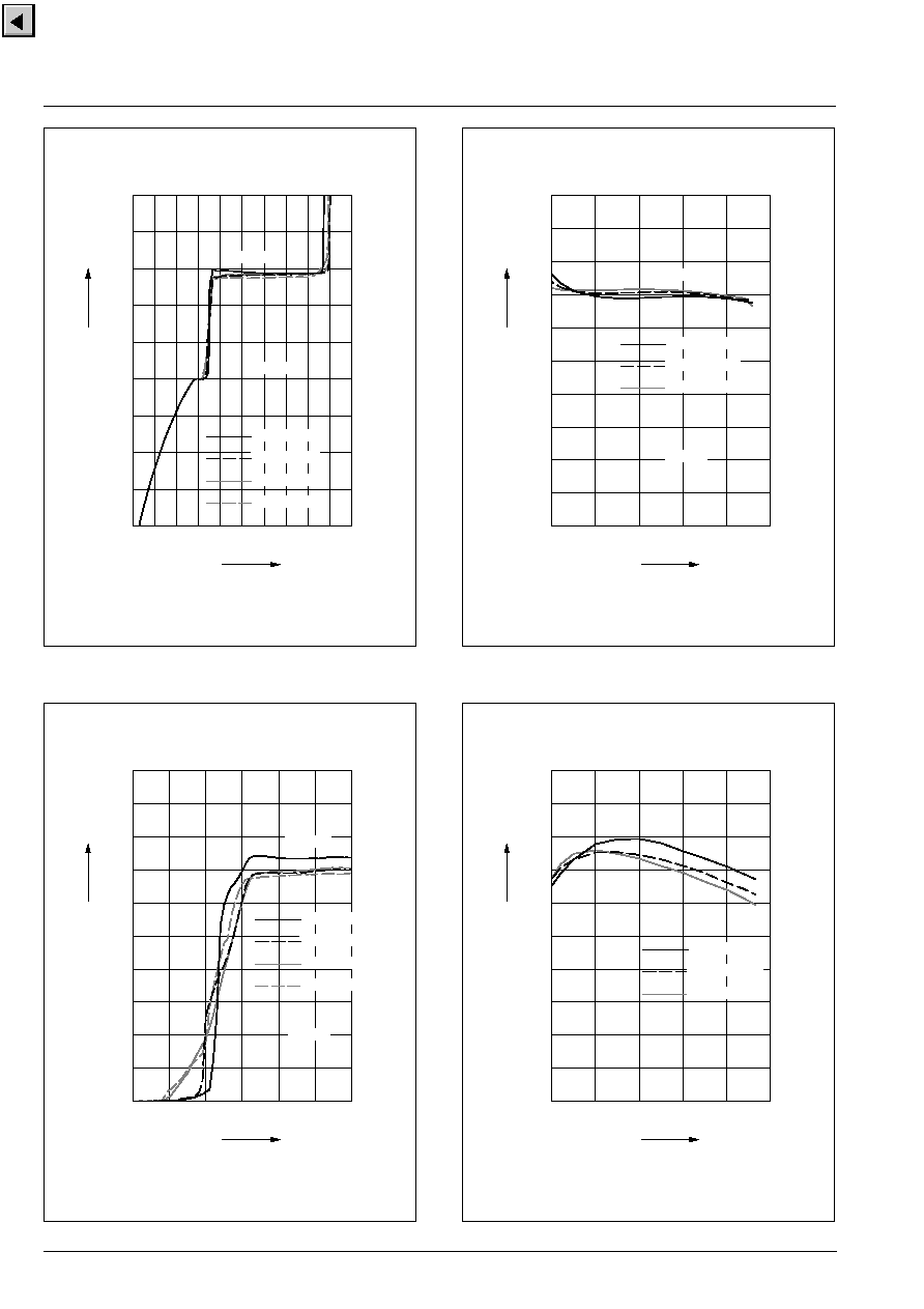
≠20
≠15
≠10
≠5
0
5
10
15
20
≠15≠10 ≠5 0
5
10 15 20 25 30 35 V
mA
V
DD
I
DD
T
A
= ≠40
∞
C
T
A
= 25
∞
C
T
A
= 100
∞
C
25
HAL 5xx
Fig. 3≠4: Typical current consumption
versus supply voltage
I
DDlow
I
DDhigh
T
A
= 170
∞
C
0
2
4
6
8
10
12
14
16
18
20
0
1
2
3
4
5
6 V
mA
V
DD
I
DD
HAL 5xx
Fig. 3≠5: Typical current consumption
versus supply voltage
I
DDlow
I
DDhigh
T
A
= ≠40
∞
C
T
A
= 25
∞
C
T
A
= 100
∞
C
T
A
= 170
∞
C
0
2
4
6
8
10
12
14
16
18
20
≠50
0
50
100
150
200
∞
C
mA
T
A
I
DD
Fig. 3≠6: Typical current consumption
versus ambient temperature
HAL 5xx
I
DDhigh
I
DDlow
V
DD
= 4 V
V
DD
= 12 V
V
DD
= 24 V
0
20
40
60
80
100
120
140
160
180
200
≠50
0
50
100
150
200
∞
C
kHz
T
A
f
osc
Fig. 3≠7: Typ. internal chopper frequency
versus ambient temperature
HAL 5xx
V
DD
= 4 V
V
DD
= 12 V
V
DD
= 24 V
HAL57x, HAL58x
ADVANCE INFORMATION
11
Micronas
0
20
40
60
80
100
120
140
160
180
200
0
5
10
15
20
25
30 V
kHz
V
DD
f
osc
Fig. 3≠8: Typ. internal chopper frequency
versus supply voltage
HAL 5xx
T
A
= ≠40
∞
C
T
A
= 25
∞
C
T
A
= 100
∞
C
T
A
= 170
∞
C
0
20
40
60
80
100
120
140
160
180
200
3
4
5
6
7
8 V
kHz
V
DD
f
osc
Fig. 3≠9: Typ. internal chopper frequency
versus supply voltage
HAL 5xx
T
A
= ≠40
∞
C
T
A
= 25
∞
C
T
A
= 100
∞
C
T
A
= 170
∞
C
HAL571
ADVANCE INFORMATION
12
Micronas
4. Type Description
4.1. HAL 571
The HAL 571 is a medium sensitive unipolar switching
sensor (see Fig. 4≠1).
The sensor turns to high current consumption with the
magnetic south pole on the branded side of the package
and turns to low current consumption if the magnetic
field is removed. It does not respond to the magnetic
north pole on the branded side.
For correct functioning in the application, the sensor re-
quires only the magnetic south pole on the branded side
of the package.
In this two-wire sensor family, the HAL 581 is a sensor
with the same magnetic characteristics but with an in-
verted output characteristic.
Magnetic Features:
≠ switching type: unipolar
≠ medium sensitivity
≠ typical B
ON
: 12 mT at room temperature
≠ typical B
OFF
: 10 mT at room temperature
≠ typical temperature coefficient of magnetic switching
points is 0 ppm/K
≠ operates with static magnetic fields and dynamic mag-
netic fields up to 10 kHz
Applications
The HAL 571 is designed for applications with one mag-
netic polarity and weak magnetic amplitudes at the sen-
sor position such as:
≠ applications with large airgap or weak magnets,
≠ solid state switches,
≠ contactless solutions to replace micro switches,
≠ position and end point detection, and
≠ rotating speed measurement.
B
HYS
Current consumption
0
B
ON
B
OFF
I
DDlow
B
Fig. 4≠1: Definition of magnetic switching points for
the HAL 571
I
DDhigh
Magnetic Characteristics at T
J
= ≠40
∞
C to +140
∞
C, V
DD
= 3.75 V to 24 V,
Typical Characteristics for V
DD
= 12 V
Magnetic flux density values of switching points.
Positive flux density values refer to the magnetic south pole at the branded side of the package.
Parameter
On point B
ON
Off point B
OFF
Hysteresis B
HYS
Magnetic Offset
Unit
T
J
Min.
Typ.
Max.
Min.
Typ.
Max.
Min.
Typ.
Max.
Min.
Typ.
Max.
≠40
∞
C
8
12
15.5
6.5
10
13.8
0.5
2
3
11
mT
25
∞
C
8
12
15.5
6.5
10
13.8
0.5
2
3
11
mT
100
∞
C
8
12
15.5
6.5
10
13.8
0.5
2
3
11
mT
140
∞
C
tbd
≠
tbd
tbd
≠
tbd
tbd
≠
tbd
tbd
mT
The hysteresis is the difference between the switching points B
HYS
= B
ON
≠ B
OFF
The magnetic offset is the mean value of the switching points B
OFFSET
= (B
ON
+ B
OFF
) / 2
HAL573
ADVANCE INFORMATION
13
Micronas
4.2. HAL 573
The HAL 573 is a low sensitive unipolar switching sensor
(see Fig. 4≠2).
The sensor turns to high current consumption with the
magnetic south pole on the branded side of the package
and turns to low current consumption if the magnetic
field is removed. It does not respond to the magnetic
north pole on the branded side.
For correct functioning in the application, the sensor re-
quires only the magnetic south pole on the branded side
of the package.
Magnetic Features:
≠ switching type: unipolar
≠ low sensitivity
≠ typical B
ON
: 43.5 mT at room temperature
≠ typical B
OFF
: 41.5 mT at room temperature
≠ typical temperature coefficient of magnetic switching
points is ≠1100 ppm/K
≠ operates with static magnetic fields and dynamic mag-
netic fields up to 10 kHz
Applications
The HAL 573 is designed for applications with one mag-
netic polarity and weak magnetic amplitudes at the sen-
sor position such as:
≠ applications with large airgap or weak magnets,
≠ solid state switches,
≠ contactless solutions to replace micro switches,
≠ position and end point detection, and
≠ rotating speed measurement.
B
HYS
Current consumption
0
B
ON
B
OFF
I
DDlow
B
Fig. 4≠2: Definition of magnetic switching points for
the HAL 573
I
DDhigh
Magnetic Characteristics at T
J
= ≠40
∞
C to +140
∞
C, V
DD
= 3.75 V to 24 V,
Typical Characteristics for V
DD
= 12 V
Magnetic flux density values of switching points.
Positive flux density values refer to the magnetic south pole at the branded side of the package.
Parameter
On point B
ON
Off point B
OFF
Hysteresis B
HYS
Magnetic Offset
Unit
T
J
Min.
Typ.
Max.
Min.
Typ.
Max.
Min.
Typ.
Max.
Min.
Typ.
Max.
≠40
∞
C
40.2
45.7
51.2
38.2
43.7
49.2
0.5
2
4
44.7
mT
25
∞
C
38
43.5
49
36
41.5
47
0.5
2
4
42.5
mT
100
∞
C
34
40
46
32
38
44
0.5
2
4
39
mT
140
∞
C
tbd
≠
tbd
tbd
≠
tbd
tbd
≠
tbd
tbd
mT
The hysteresis is the difference between the switching points B
HYS
= B
ON
≠ B
OFF
The magnetic offset is the mean value of the switching points B
OFFSET
= (B
ON
+ B
OFF
) / 2
HAL574
ADVANCE INFORMATION
14
Micronas
4.3. HAL 574
The HAL 574 is a medium sensitive unipolar switching
sensor (see Fig. 4≠3).
The sensor turns to high current consumption with the
magnetic south pole on the branded side of the package
and turns to low current consumption if the magnetic
field is removed. It does not respond to the magnetic
north pole on the branded side.
For correct functioning in the application, the sensor re-
quires only the magnetic south pole on the branded side
of the package.
In this two-wire sensor family, the HAL 584 is a sensor
with the same magnetic characteristics but with an in-
verted output characteristic.
Magnetic Features:
≠ switching type: unipolar
≠ medium sensitivity
≠ typical B
ON
: 9.2 mT at room temperature
≠ typical B
OFF
: 7.2 mT at room temperature
≠ typical temperature coefficient of magnetic switching
points is 0 ppm/K
≠ operates with static magnetic fields and dynamic mag-
netic fields up to 10 kHz
Applications
The HAL 574 is designed for applications with one mag-
netic polarity and weak magnetic amplitudes at the sen-
sor position such as:
≠ applications with large airgap or weak magnets,
≠ solid state switches,
≠ contactless solutions to replace micro switches,
≠ position and end point detection, and
≠ rotating speed measurement.
B
HYS
Current consumption
0
B
ON
B
OFF
I
DDlow
B
Fig. 4≠3: Definition of magnetic switching points for
the HAL 574
I
DDhigh
Magnetic Characteristics at T
J
= ≠40
∞
C to +170
∞
C, V
DD
= 3.75 V to 24 V,
Typical Characteristics for V
DD
= 12 V
Magnetic flux density values of switching points.
Positive flux density values refer to the magnetic south pole at the branded side of the package.
Parameter
On point B
ON
Off point B
OFF
Hysteresis B
HYS
Magnetic Offset
Unit
T
J
Min.
Typ.
Max.
Min.
Typ.
Max.
Min.
Typ.
Max.
Min.
Typ.
Max.
≠40
∞
C
5.5
9.2
12
5
7.2
11.5
0.5
2
3
8.2
mT
25
∞
C
5.5
9.2
12
5
7.2
11.5
0.5
2
3
8.2
mT
100
∞
C
5.5
9.2
12
5
7.2
11.5
0.5
2
3
8.2
mT
140
∞
C
tbd
≠
tbd
tbd
≠
tbd
tbd
≠
tbd
tbd
mT
The hysteresis is the difference between the switching points B
HYS
= B
ON
≠ B
OFF
The magnetic offset is the mean value of the switching points B
OFFSET
= (B
ON
+ B
OFF
) / 2
HAL575
ADVANCE INFORMATION
15
Micronas
4.4. HAL 575
The HAL 575 is a medium sensitive latching switching
sensor (see Fig. 4≠4).
The sensor turns to high current consumption with the
magnetic south pole on the branded side of the package
and turns to low consumption with the magnetic north
pole on the branded side. The current consumption does
not change if the magnetic field is removed. For chang-
ing the current consumption, the opposite magnetic field
polarity must be applied.
For correct functioning in the application, the sensor re-
quires both magnetic polaritys on the branded side of the
package.
Magnetic Features:
≠ switching type: latching
≠ medium sensitivity
≠ typical B
ON
: 4 mT at room temperature
≠ typical B
OFF
: ≠4 mT at room temperature
≠ typical temperature coefficient of magnetic switching
points is 0 ppm/K
≠ operates with static magnetic fields and dynamic mag-
netic fields up to 10 kHz
Applications
The HAL 575 is designed for applications with both mag-
netic polaritys and weak magnetic amplitudes at the
sensor position such as:
≠ applications with large airgap or weak magnets,
≠ multipole magnet applications,
≠ contactless solutions to replace micro switches,
≠ rotating speed measurement.
B
HYS
Current consumption
0
B
ON
B
OFF
I
DDlow
B
Fig. 4≠4: Definition of magnetic switching points for
the HAL 575
I
DDhigh
Magnetic Characteristics at T
J
= ≠40
∞
C to +140
∞
C, V
DD
= 3.75 V to 24 V,
Typical Characteristics for V
DD
= 12 V
Magnetic flux density values of switching points.
Positive flux density values refer to the magnetic south pole at the branded side of the package.
Parameter
On point B
ON
Off point B
OFF
Hysteresis B
HYS
Magnetic Offset
Unit
T
J
Min.
Typ.
Max.
Min.
Typ.
Max.
Min.
Typ.
Max.
Min.
Typ.
Max.
≠40
∞
C
0.5
4
8
≠8
≠4
≠0.5
5
8
11
0
mT
25
∞
C
0.5
4
8
≠8
≠4
≠0.5
5
8
11
0
mT
100
∞
C
0.5
4
8
≠8
≠4
≠0.5
5
8
11
0
mT
140
∞
C
tbd
≠
tbd
tbd
≠
tbd
tbd
≠
tbd
tbd
mT
The hysteresis is the difference between the switching points B
HYS
= B
ON
≠ B
OFF
The magnetic offset is the mean value of the switching points B
OFFSET
= (B
ON
+ B
OFF
) / 2
HAL581
ADVANCE INFORMATION
16
Micronas
4.5. HAL 581
The HAL 581 is a medium sensitive unipolar switching
sensor with an inverted output (see Fig. 4≠5).
The sensor turns to low current consumption with the
magnetic south pole on the branded side of the package
and turns to high current consumption if the magnetic
field is removed. It does not respond to the magnetic
north pole on the branded side.
For correct functioning in the application, the sensor re-
quires only the magnetic south pole on the branded side
of the package.
In this two-wire sensor family, the HAL 571 is a sensor
with the same magnetic characteristics but with a normal
output characteristic.
Magnetic Features:
≠ switching type: unipolar inverted
≠ medium sensitivity
≠ typical B
ON
: 10 mT at room temperature
≠ typical B
OFF
: 12 mT at room temperature
≠ typical temperature coefficient of magnetic switching
points is 0 ppm/K
≠ operates with static magnetic fields and dynamic mag-
netic fields up to 10 kHz
Applications
The HAL 581 is designed for applications with one mag-
netic polarity and weak magnetic amplitudes at the sen-
sor position where an inverted output signal is required
such as:
≠ applications with large airgap or weak magnets,
≠ solid state switches,
≠ contactless solutions to replace micro switches,
≠ position and end point detection, and
≠ rotating speed measurement.
B
HYS
0
B
OFF
B
ON
B
Fig. 4≠5: Definition of magnetic switching points for
the HAL 581
I
DDhigh
I
DDlow
Current consumption
Magnetic Characteristics at T
J
= ≠40
∞
C to +140
∞
C, V
DD
= 3.75 V to 24 V,
Typical Characteristics for V
DD
= 12 V
Magnetic flux density values of switching points.
Positive flux density values refer to the magnetic south pole at the branded side of the package.
Parameter
On point B
ON
Off point B
OFF
Hysteresis B
HYS
Magnetic Offset
Unit
T
J
Min.
Typ.
Max.
Min.
Typ.
Max.
Min.
Typ.
Max.
Min.
Typ.
Max.
≠40
∞
C
6.5
10
13.8
8
12
15.5
0.5
2
3
11
mT
25
∞
C
6.5
10
13.8
8
12
15.5
0.5
2
3
11
mT
100
∞
C
6.5
10
13.8
8
12
15.5
0.5
2
3
11
mT
140
∞
C
tbd
≠
tbd
tbd
≠
tbd
tbd
≠
tbd
tbd
mT
The hysteresis is the difference between the switching points B
HYS
= B
OFF
≠ B
ON
The magnetic offset is the mean value of the switching points B
OFFSET
= (B
ON
+ B
OFF
) / 2

HAL584
ADVANCE INFORMATION
17
Micronas
4.6. HAL 584
The HAL 584 is a medium sensitive unipolar switching
sensor with an inverted output (see Fig. 4≠6).
The sensor turns to low current consumption with the
magnetic south pole on the branded side of the package
and turns to high current consumption if the magnetic
field is removed. It does not respond to the magnetic
north pole on the branded side.
For correct functioning in the application, the sensor re-
quires only the magnetic south pole on the branded side
of the package.
In this two-wire sensor family, the HAL 574 is a sensor
with the same magnetic characteristics but with a normal
output characteristic.
Magnetic Features:
≠ switching type: unipolar inverted
≠ medium sensitivity
≠ typical B
ON
: 7.2 mT at room temperature
≠ typical B
OFF
: 9.2 mT at room temperature
≠ typical temperature coefficient of magnetic switching
points is 0 ppm/K
≠ operates with static magnetic fields and dynamic mag-
netic fields up to 10 kHz
Applications
The HAL 584 is designed for applications with one mag-
netic polarity and weak magnetic amplitudes at the sen-
sor position where an inverted output signal is required
such as:
≠ applications with large airgap or weak magnets,
≠ solid state switches,
≠ contactless solutions to replace micro switches,
≠ position and end point detection, and
≠ rotating speed measurement.
B
HYS
0
B
OFF
B
ON
B
Fig. 4≠6: Definition of magnetic switching points for
the HAL 584
I
DDhigh
I
DDlow
Current consumption
Magnetic Characteristics at T
J
= ≠40
∞
C to +140
∞
C, V
DD
= 3.75 V to 24 V,
Typical Characteristics for V
DD
= 12 V
Magnetic flux density values of switching points.
Positive flux density values refer to the magnetic south pole at the branded side of the package.
Parameter
On point B
ON
Off point B
OFF
Hysteresis B
HYS
Magnetic Offset
Unit
T
J
Min.
Typ.
Max.
Min.
Typ.
Max.
Min.
Typ.
Max.
Min.
Typ.
Max.
≠40
∞
C
5
7.2
11.5
5.5
9.2
12
0.5
2
3
8.2
mT
25
∞
C
5
7.2
11.5
5.5
9.2
12
0.5
2
3
8.2
mT
100
∞
C
5
7.2
11.5
5.5
9.2
12
0.5
2
3
8.2
mT
140
∞
C
tbd
≠
tbd
tbd
≠
tbd
tbd
≠
tbd
tbd
mT
The hysteresis is the difference between the switching points B
HYS
= B
OFF
≠ B
ON
The magnetic offset is the mean value of the switching points B
OFFSET
= (B
ON
+ B
OFF
) / 2

HAL57x, HAL 58x
ADVANCE INFORMATION
18
Micronas
5. Application Notes
5.1. Application Circuit
Figure 5≠1 shows a simple application with a two-wire
sensor. The current consumption can be detected by
measuring the voltage over R
L
. For correct functioning
of the sensor, the voltage between pin 1 and 2 (V
DD
)
must be a minimum of 3.75 V. With the maximum current
consumption of 17 mA, the maximum R
L
can be calcu-
lated as:
R
Lmax
+
V
SUPmin
*
3.75 V
17 mA
V
SUP
R
L
1 V
DD
GND
2 or 3
V
SIG
Fig. 5≠1: Application Circuit 1
For applications with disturbances on the supply line or
radiated disturbances, a series resistor R
V
(ranging from
10
to 30
)
and a capacitor both placed close to the
sensor are recommended (see figure 5≠2). In this case,
the maximum R
L
can be calculated as:
R
Lmax
+
V
SUPmin
*
3.75 V
17 mA
*
R
V
1 V
DD
GND
2 or 3
Fig. 5≠2: Application Circuit 2
4.7 nF
R
V
V
SUP
R
L
V
SIG
5.2. Extended Operating Conditions
All sensors fulfill the electrical and magnetic characteris-
tics when operated within the Recommended Operating
Conditions (see page 7).
Typically, the sensors operate with supply voltages
above 3 V. However, below 3.75 V, the current consump-
tion and the magnetic characteristics may be outside the
specification.
Note: The functionality of the sensor below 3.75 V is not
tested on a regular base. For special test conditions,
please contact Micronas.
5.3. Start-up Behavior
Due to the active offset compensation, the sensors have
an initialization time (enable time t
en(O)
) after applying
the supply voltage. The parameter t
en(O)
is specified in
the Electrical Characteristics (see page 8). During the
initialization time, the current consumption is not defined
and can toggle between low and high.
HAL 57x:
After t
en(O)
, the current consumption will be high if the
applied magnetic field B is above B
ON
. The current con-
sumption will be low if B is below B
OFF
.
HAL 58x
In case of sensors with an inverted switching behavior,
the current consumption will be low if B > B
OFF
and high
if B < B
ON
.
Note: For magnetic fields between B
OFF
and B
ON
, the
current consumption of the HAL sensor will be either low
or high after applying V
DD
. In order to achieve a defined
current consumption, the applied magnetic field must be
above B
ON
, respectively, below B
OFF
.
HAL57x, HAL58x
ADVANCE INFORMATION
19
Micronas
5.4. Ambient Temperature
Due to internal power dissipation, the temperature on
the silicon chip (junction temperature T
J
) is higher than
the temperature outside the package (ambient tempera-
ture T
A
).
T
J
= T
A
+
T
At static conditions and continuous operation, the follow-
ing equation is valid:
T = I
DD
* V
DD
* R
th
For all sensors, the junction temperature range T
J
is
specified. The maximum ambient temperature T
Amax
can be calculated as:
T
Amax
= T
Jmax
≠
T
For typical values, use the typical parameters. For worst
case calculation, use the max. parameters for I
DD
and
R
th
, and the max. value for V
DD
from the application.
Due to the range of I
DDhigh
, self-heating can be critical.
The junction temperature can be reduced with pulsed
supply voltage. For supply times (t
on
) ranging from 30
µ
s
to 1 ms, the following equation can be used:
D
T
+
I
DD
* V
DD
* R
th
*
t
on
t
off
)
t
on
5.5. EMC and ESD
For applications with disturbances on the supply line or
radiated disturbances, a series resistor and a capacitor
are recommended (see Fig. 5≠2). The series resistor
and the capacitor should be placed as closely as pos-
sible to the HAL sensor.
Please contact Micronas for detailed information and
first EMC and ESD results.
4.7 nF
V
EMC
R
V1
100
GND
2, 3
1 V
DD
R
V2
30
Fig. 5≠3: Recommended EMC test circuit

HAL57x, HAL58x
ADVANCE INFORMATION
20
Micronas
6. Data Sheet History
1. Advanced Information: "HAL 571, 573... 575, 581,
584 Two-Wire Hall Effect Sensor Family", Oct. 11,
2000, 6251-538-1AI. First release of the advance
information.
Micronas GmbH
Hans-Bunte-Strasse 19
D-79108 Freiburg (Germany)
P.O. Box 840
D-79008 Freiburg (Germany)
Tel. +49-761-517-0
Fax +49-761-517-2174
E-mail: docservice@micronas.com
Internet: www.micronas.com
Printed in Germany
Order No. 6251-538-1AI
All information and data contained in this data sheet are without any
commitment, are not to be considered as an offer for conclusion of a
contract, nor shall they be construed as to create any liability. Any new
issue of this data sheet invalidates previous issues. Product availability
and delivery are exclusively subject to our respective order confirma-
tion form; the same applies to orders based on development samples
delivered. By this publication, Micronas GmbH does not assume re-
sponsibility for patent infringements or other rights of third parties
which may result from its use.
Further, Micronas GmbH reserves the right to revise this publication
and to make changes to its content, at any time, without obligation to
notify any person or entity of such revisions or changes.
No part of this publication may be reproduced, photocopied, stored on
a retrieval system, or transmitted without the express written consent
of Micronas GmbH.