HAL710
Hall-Effect Sensor
with Direction Detection
Edition Feb. 20, 2001
6251-478-1AI
ADVANCE INFORMATION
MICRONAS
MICRONAS

HAL710
ADVANCE INFORMATION
2
Micronas
Contents
Page
Section
Title
3
1.
Introduction
3
1.1.
Features
3
1.2.
Applications
4
1.3.
Marking Code
4
1.3.1.
Special Marking of Prototype Parts
4
1.4.
Operating Junction Temperature Range
4
1.5.
Hall Sensor Package Codes
4
1.6.
Solderability
5
2.
Functional Description
7
3.
Specifications
7
3.1.
Outline Dimensions
7
3.2.
Dimensions of Sensitive Areas
7
3.3.
Positions of Sensitive Areas
8
3.4.
Absolute Maximum Ratings
8
3.5.
Recommended Operating Conditions
9
3.6.
Electrical Characteristics
10
3.7.
Magnetic Characteristics
10
3.7.1.
Magnetic Thresholds
10
3.7.2.
Matching B
S1
and B
S2
10
3.7.3.
Hysteresis Matching
11
4.
Application Notes
11
4.1.
Ambient Temperature
11
4.2.
Extended Operating Conditions
11
4.3.
Signal Delay
11
4.4.
Test Mode Activation
11
4.5.
Start-up Behavior
12
4.6.
EMC and ESD
12
5.
Data Sheet History

ADVANCE INFORMATION
HAL710
Micronas
3
Hall-Effect Sensor with Direction Detection
1. Introduction
The HAL 710 is a monolithic integrated Hall-effect sen-
sor manufactured in CMOS technology with two inde-
pendent Hall plates S1 and S2 spaced 2.35 mm apart.
The device has two open-drain outputs:
The 'Count Output' operates like a single latched Hall
switch according to the magnetic field present at Hall
plate S1 (see Fig. 3≠3).
The `Direction Output' indicates the direction of a linear
or rotating movement of magnetic objects.
In combination with an active target providing a
sequence of alternating magnetic north and south
poles, the sensor forms a system generating the sig-
nals required to control position, speed, and direction
of the target movement.
The internal circuitry evaluates the direction of the
movement and updates the `Direction Output' at every
edge of the `Count Signal' (rising and falling). The
Direction Output is high if the target moves from Hall
plate S1 to Hall plate S2. It is low if the target first
passes plate S2 and later plate S1. The state of the
Direction Output only changes at a rising or falling
edge of the Count Output.
The design ensures a setup time for the Direction Out-
put with respect to the corresponding Count Signal
edge of 1/2 clock periods (1
µ
s minimum).
The device includes temperature compensation and
active offset compensation. These features provide
excellent stability and matching of the switching points
in the presence of mechanical stress over the whole
temperature and supply voltage range. This is required
by systems determining the direction from the compar-
ison of two transducer signals.
The sensor is designed for industrial and automotive
applications and operates with supply voltages from
3.8 V to 24 V in the ambient temperature range from
-
40
∞
C up to 125
∞
C.
The HAL 710 is available in the SMD package
SOT-89B.
1.1. Features
≠ generation of `Count Signals' and `Direction Signals'
≠ delay of the `Count Signals' with respect to the
`Direction Signal' of 1
µ
s minimum
≠ switching type latching
≠ low sensitivity
≠ typical B
ON
: 14.9 mT at room temperature
≠ typical B
OFF
:
-
14.9 mT at room temperature
≠ temperature coefficient of
-
2000 ppm/K in all mag-
netic characteristics
≠ switching offset compensation at typically 150 kHz
≠ operation from 3.8 V to 24 V supply voltage
≠ operation with static magnetic fields and dynamic
magnetic fields up to 10 kHz
≠ overvoltage protection at all pins
≠ reverse-voltage protection at V
DD
-pin
≠ robustness of magnetic characteristics against
mechanical stress
≠ short-circuit protected open-drain outputs by ther-
mal shut down
≠ constant switching points over a wide supply voltage
range
≠ EMC corresponding to DIN 40839
1.2. Applications
The HAL 710 is the optimal sensor for position-control
applications with direction detection and alternating
magnetic signals such as:
≠ multipole magnet applications,
≠ rotating speed and direction measurement,
position tracking (active targets), and
≠ window lifters.
HAL710
ADVANCE INFORMATION
4
Micronas
1.3. Marking Code
All Hall sensors have a marking on the package sur-
face (branded side). This marking includes the name
of the sensor and the temperature range.
1.3.1. Special Marking of Prototype Parts
Prototype parts are coded with an underscore beneath
the temperature range letter on each IC. They may be
used for lab experiments and design-ins but are not
intended to be used for qualification test or as produc-
tion parts.
1.4. Operating Junction Temperature Range
The Hall sensors from Micronas are specified to the
chip temperature (junction temperature T
J
).
K: T
J
=
-
40
∞
C to +140
∞
C
E: T
J
=
-
40
∞
C to +100
∞
C
The relationship between ambient temperature (T
A
)
and junction temperature is explained in Section 4.1.
on page 11.
1.5. Hall Sensor Package Codes
Hall sensors are available in a wide variety of packag-
ing quantities. For more detailed information, please
refer to the brochure: "Ordering Codes for Hall Sen-
sors".
1.6. Solderability
All packages: according to IEC68-2-58
During soldering, reflow processing and manual
reworking, a component body temperature of 260
∞
C
should not be exceeded.
Components stored in the original packaging should
provide a shelf life of at least 12 months, starting from
the date code printed on the labels, even in environ-
ments as extreme as 40
∞
C and 90% relative humidity.
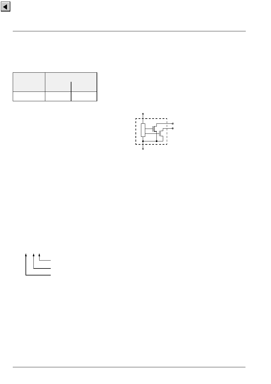
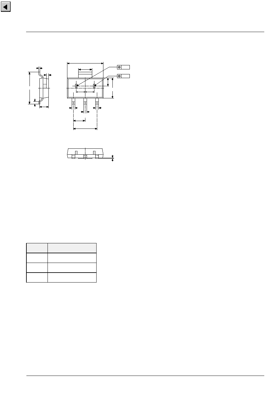
Fig. 1≠1: Pin configuration
Type
Temperature Range
K
E
HAL710
710K
710E
HALXXXPA-T
Temperature Range: K, or E
Package: SF for SOT-89B
Type: 710
Example: HAL 710SF-K
Type: 710
Package: SOT-89B
Temperature Range: T
J
=
-
40
∞
C to +140
∞
C
1 V
DD
4
GND
3 Count Output
2 Direction Output
ADVANCE INFORMATION
HAL710
Micronas
5
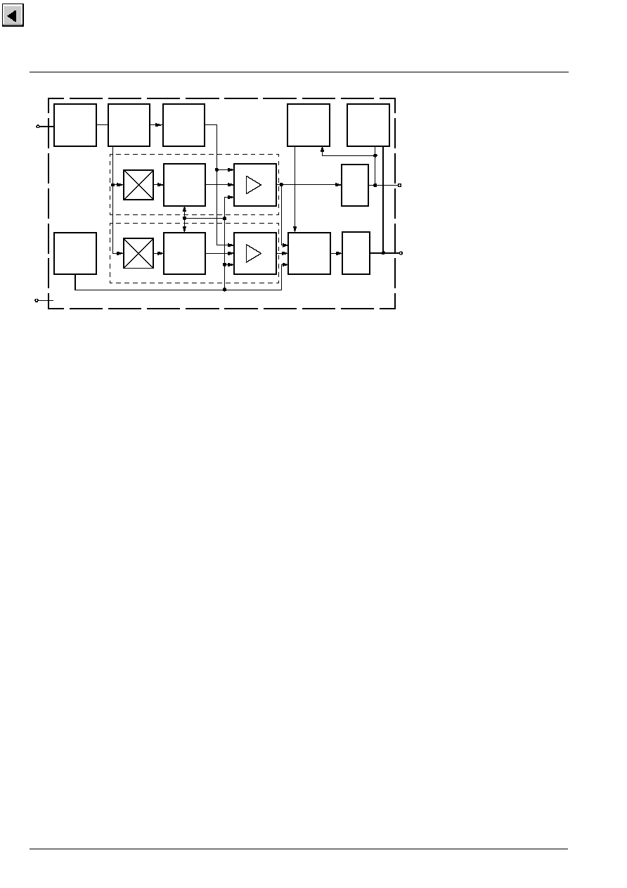
2. Functional Description
The HAL 710 is a monolithic integrated circuit with two
independent subblocks consisting each of a Hall plate
and the corresponding comparator. Each subblock
independently switches the comparator output in
response to the magnetic field at the location of the
corresponding sensitive area. If a magnetic field with
flux lines perpendicular to the sensitive area is
present, the biased Hall plate generates a Hall voltage
proportional to this field. The Hall voltage is compared
with the actual threshold level in the comparator. The
subblocks are designed to have closely matched
switching points.
The temperature-dependent bias ≠ common to both
subblocks ≠ increases the supply voltage of the Hall
plates and adjusts the switching points to the decreas-
ing induction of magnets at higher temperatures. If the
magnetic field exceeds the threshold levels, the com-
parator switches to the appropriate state. The built-in
hysteresis prevents oscillations of the outputs.
In order to achieve good matching of the switching
points of both subblocks, the magnetic offset caused
by mechanical stress is compensated for by use of
"switching offset compensation techniques". Therefore,
an internal oscillator provides a two-phase clock to
both subblocks. For each subblock the Hall voltage is
sampled at the end of the first phase. At the end of the
second phase, both sampled and actual Hall voltages
are averaged and compared with the actual switching
point.
The output of comparator 1 (connected to S1) directly
controls the `Count Output'. The outputs of both com-
parators enter the `Direction Detection Block' control-
ling the state of the `Direction Output'. The `Direction
Output' is 'high' if the edge at the output of
comparator 1 precedes that at comparator 2. In the
opposite case, `Direction Output' is 'low'. The previous
state of the `Direction Output' is maintained between
edges of the `Count Output' and in case the edges at
comparator 1 and comparator 2 occur in the same
clock period.
Shunt protection devices clamp voltage peaks at the
output pins and V
DD
-pin together with external series
resistors. Reverse current is limited at the V
DD
-pin by
an internal series resistor up to
-
15 V. No external
reverse protection diode is needed at the V
DD
-pin for
reverse voltages ranging from 0 V to
-
15 V.
Fig. 2≠1: Timing diagram
I
dd
t
Direction
t
V
OH
V
OL
Count
t
V
OH
V
OL
B
S2
t
B
S2on
Clock
t
1/f
osc
t
f
Output
Output
B
S1
BS1
on
I
dd
HAL710
ADVANCE INFORMATION
6
Micronas
Fig. 2≠2: HAL 710 block diagram
Reverse
Voltage and
Overvoltage
Protection
Temperature
Dependent
Bias
Hysteresis
Control
Hall Plate 1
Switch
Comparator
1
V
DD
Hall Plate 2
Switch
Comparator
Clock
Output
3
Count Output
Direction
Output
2
Direction Output
Short Circuit
and
Overvoltage
Protection
Test-Mode
Control
S1
S2
Detection
GND
4
ADVANCE INFORMATION
HAL710
Micronas
7
3. Specifications
3.1. Outline Dimensions
Fig. 3≠1:
Plastic Small Outline Transistor Package
(SOT-89B)
Weight approximately 0.035 g
Dimensions in mm
3.2. Dimensions of Sensitive Areas
Dimensions: 0.25 mm
◊
0.12 mm
3.3. Positions of Sensitive Areas
Note: For all package diagrams, a mechanical toler-
ance of
±
0.05 mm applies to all dimensions where no
tolerance is explicitly given.
SOT-89B
x
1
+
x
2
(2.35
±
0.001) mm
x
1
=
x
2
1.175 mm nominal
y
0.975 mm nominal
sensitive area S
1
min.
0.25
x
1
x
2
2.55
0.4
0.4
0.4
1.5
3.0
0.06
±
0.04
4
±
0.2
0.15
branded side
SPGS0022-5-B4/1E
top view
y
1
2
3
4
0.3
1.15
0.2
sensitive area S
2
0.2
4.55
1.7
HAL710
ADVANCE INFORMATION
8
Micronas
3.4. Absolute Maximum Ratings
Stresses beyond those listed in the "Absolute Maximum Ratings" may cause permanent damage to the device. This
is a stress rating only. Functional operation of the device at these or any other conditions beyond those indicated in
the "Recommended Operating Conditions/Characteristics" of this specification is not implied. Exposure to absolute
maximum ratings conditions for extended periods may affect device reliability.
3.5. Recommended Operating Conditions
Symbol
Parameter
Pin No.
Min.
Max.
Unit
V
DD
Supply Voltage
1
-
15
28
1)
V
-V
P
Supply Voltage
1
-
24
2)
28
1)
V
-
I
DD
Reverse Supply Current
1
-
50
1)
mA
I
DDZ
Supply Current through Protection
Device
1
-
100
3)
100
3)
mA
V
O
Output Voltage
2, 3
-
0.3
28
1)
V
I
O
Continuous Output On Current
2, 3
-
20
1)
mA
I
Omax
Peak Output On Current
2, 3
-
150
3)
mA
I
OZ
Output Current through Protection
Device
3
-
200
3)
200
3)
mA
T
S
Storage Temperature Range
-
65
150
5)
∞C
T
J
Junction Temperature Range
-
40
-
40
170
4)
150
∞C
∞C
1)
as long, as T
Jmax
is not exceeded
2)
with a 220-
series resistance at pin 1 corresponding to test circuit 1
3)
t < 2 ms
4)
t < 1000 h
5)
Components stored in the original packaging should provide a shelf life of at least 12 months, starting from the
date code printed on the labels, even in environments as extreme as 40
∞
C and 90% relative humidity.
Symbol
Parameter
Pin No.
Min.
Typ.
Max.
Unit
V
DD
Supply Voltage
1
3.8
-
24
V
I
O
Continuous Output Current
3
0
-
10
mA
V
O
Output Voltage
(output switch off)
3
0
-
24
V

ADVANCE INFORMATION
HAL710
Micronas
9
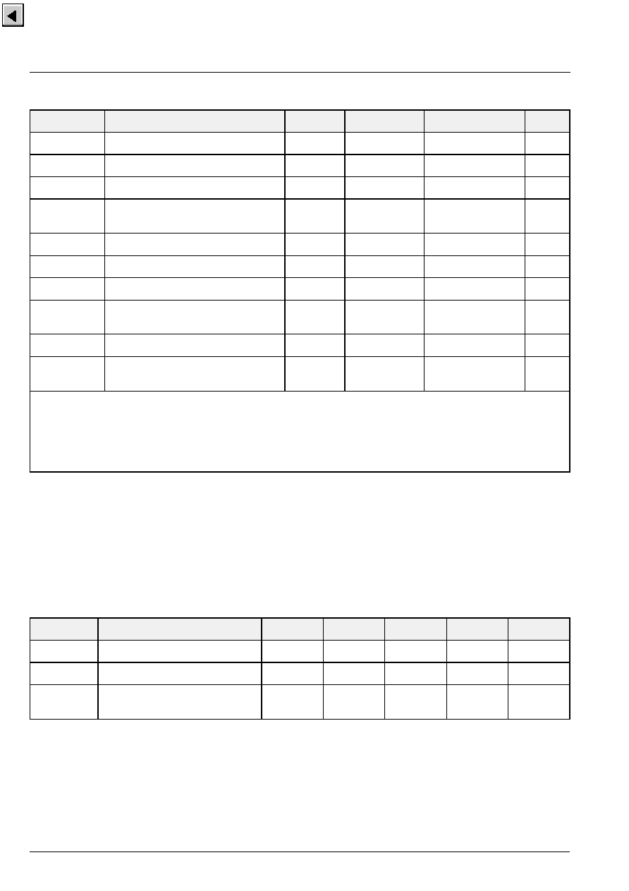
3.6. Electrical Characteristics
at T
J
=
-
40 ∞C to +140 ∞C, V
DD
= 3.8 V to 24 V, as not otherwise specified in Conditions.
Typical Characteristics for T
J
= 25 ∞C and V
DD
= 5 V.
Fig. 3≠2: Recommended pad size for SOT-89B
Dimensions in mm
Symbol
Parameter
Pin No.
Min.
Typ.
Max.
Unit
Conditions
I
DD
Supply Current
1
2
5.5
9
mA
T
J
= 25 ∞C
I
DD
Supply Current
over Temperature Range
1
7
10
mA
V
DDZ
Overvoltage Protection
at Supply
1
28.5
32
V
I
DD
= 25 mA, T
J
= 25 ∞C, t = 20 ms
V
OZ
Overvoltage Protection
at Output
2,3
28
32
V
I
OH
= 25 mA, T
J
= 25 ∞C, t = 20 ms
V
OL
Output Voltage
2,3
130
280
mV
I
OL
= 10 mA, T
J
= 25 ∞C
V
OL
Output Voltage over
Temperature Range
2,3
130
400
mV
I
OL
= 10 mA,
I
OH
Output Leakage Current
2,3
0.06
0.1
µ
A
Output switched off, T
J
= 25 ∞C,
V
OH
= 3.8 V to 24 V
I
OH
Output Leakage Current over
Temperature Range
2,3
-
10
µ
A
Output switched off, T
J
140 ∞C,
V
OH
= 3.8 V to 24 V
f
osc
Internal sampling frequency
-
130
150
-
kHz
T
J
= 25 ∞C
f
osc
Internal sampling frequency
over Temperature Range
-
100
150
-
kHz
t
en
(O)
Enable Time of Output after
Setting of V
DD
50
100
µ
s
V
DD
= 12 V,
B>B
on
+ 2 mT or B<B
off
-
2 mT
t
r
Output Rise Time
2,3
1.2
µ
s
V
DD
= 12 V, R
L
= 20 k
,
C
L
= 20 pF
t
f
Output FallTime
2,3
0.2
1.6
µ
s
V
DD
= 12 V, R
L
= 20 k
,
C
L
= 20 pF
R
thSB
SOT-89B
Thermal Resistance Junction to
Substrate Backside
-
-
150
200
K/W
Fiberglass Substrate
30 mm x 10mm x 1.5mm,
pad size see Fig. 3≠2
5.0
2.0
2.0
1.0
HAL710
ADVANCE INFORMATION
10
Micronas
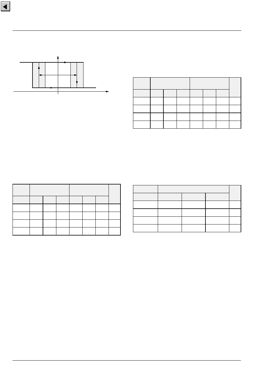
3.7. Magnetic Characteristics
Fig. 3≠3: Definition of magnetic switching points for
the HAL710
Positive flux density values refer to magnetic south
pole at the branded side of the package.
3.7.1. Magnetic Thresholds
(quasistationary: dB/dt<0.5 mT/ms)
at T
J
=
-
40 ∞C to +140 ∞C, V
DD
= 3.8 V to 24 V, as not
otherwise specified
Typical Characteristics for T
J
= 25 ∞C and V
DD
= 5 V
3.7.2. Matching B
S1
and B
S2
(quasistationary: dB/dt<0.5 mT/ms)
at T
J
=
-
40 ∞C to +140 ∞C, V
DD
= 3.8 V to 24 V, as not
otherwise specified
Typical Characteristics for T
J
= 25 ∞C and V
DD
= 5 V
3.7.3. Hysteresis Matching
(quasistationary: dB/dt<0.5 mT/ms)
at T
J
=
-
40 ∞C to +140 ∞C, V
DD
= 3.8 V to 24 V, as not
otherwise specified
Typical Characteristics for T
J
= 25 ∞C and V
DD
= 5 V
Para-
meter
On point
B
S1on,
B
S2on
Off point
B
S1off,
, B
S2off
Unit
T
j
Min.
Typ.
Max.
Min.
Typ.
Max.
-
40 ∞C
12.5
16.3
20
-
20
-
16.3
-
12.5
mT
25 ∞C
10.7
14.9
19.1
-
19.1
-
14.9
-
10.7
mT
100 ∞C
tbd
tbd
tbd
tbd
tbd
tbd
mT
140 ∞C
6.0
10.9
16.0
-
16.0
-
10.9
-
6.0
mT
B
OFF
B
ON
0
V
OL
V
O
Output Voltage
B
B
HYS
Para-
meter
B
S1on
-
B
S2on
B
S1off
-
B
S2off
Unit
T
j
Min.
Typ
Max.
Min.
Typ
Max.
-
40 ∞C
-
7.5
0
7.5
-
7.5
0
7.5
mT
25 ∞C
-
7.5
0
7.5
-
7.5
0
7.5
mT
100 ∞C
-
7.5
0
7.5
-
7.5
0
7.5
mT
140 ∞C
-
7.5
0
7.5
-
7.5
0
7.5
mT
Parameter
(B
S1on
-
B
S1off
) / (B
S2on
-
B
S2off
)
Unit
T
j
Min.
Typ.
Max.
-
40 ∞C
0.85
1.0
1.2
-
25 ∞C
0.85
1.0
1.2
-
100 ∞C
0.85
1.0
1.2
-
140 ∞C
0.85
1.0
1.2
-

ADVANCE INFORMATION
HAL710
Micronas
11
4. Application Notes
4.1. Ambient Temperature
Due to the internal power dissipation, the temperature
on the silicon chip (junction temperature T
J
) is higher
than the temperature outside the package (ambient
temperature T
A
).
T
J
= T
A
+
T
At static conditions, the following equation is valid:
T = I
DD
* V
DD
* R
th
For typical values, use the typical parameters. For
worst case calculation, use the max. parameters for
I
DD
and R
th
, and the max. value for V
DD
from the appli-
cation.
For all sensors, the junction temperature range T
J
is
specified. The maximum ambient temperature T
Amax
can be calculated as:
T
Amax
= T
Jmax
-
T
4.2. Extended Operating Conditions
All sensors fulfil the electrical and magnetic character-
istics when operated within the Recommended Oper-
ating Conditions (see page 8)
Supply Voltage Below 3.8 V
Typically, the sensors operate with supply voltages
above 3 V, however, below 3.8 V some characteristics
may be outside the specification.
Note: The functionality of the sensor below 3.8 V is not
tested. For special test conditions, please contact Mic-
ronas.
4.3. Signal Delay
The extra circuitry required for the direction detection
increases the latency of the `Count and Direction Sig-
nal' compared to a simple switch (e.g. HAL 525). This
extra delay corresponds to 0.5 and 1 clock period for
the `Direction Signal' and `Count Signal' respectively.
4.4. Test Mode Activation
In order to obtain the normal operation as described
above, two external pull-up resistors with appropriate
values are required to connect each output to an exter-
nal supply, such that the potential at the open-drain
output rises to at least 3 V in less than 10
µ
s after hav-
ing turned off the corresponding pull-down transistor or
after having applied V
DD
.
If the `Direction Output' is pulled low externally (the
potential does not rise after the internal pull-down tran-
sistor has been turned off), the device enters Manufac-
turer Test Mode.
Direction Detection is not functional in Manufacturer
Test Mode. The device returns to `Normal Operation'
as soon as the `Count Output' goes high.
Please note, that the presence of a Manufacturer Test
Mode requires appropriate measures to prevent acci-
dental activation (e.g. in response to EMC events).
4.5. Start-up Behavior
Due to the active offset compensation, the sensors
have an initialization time (enable time t
en(O)
) after
applying the supply voltage. The parameter t
en(O)
is
specified in the Electrical Characteristics (see page 9)
During the initialization time, the output states are not
defined and the outputs can toggle. After t
en(O)
both
outputs will be either high or low for a stable magnetic
field (no toggling) and the `Count Output' will be low if
the applied magnetic field B exceeds B
ON
. The `Count
Output' will be high if B drops below B
OFF
. The `Direc-
tion Output' will have the correct state after the second
edge (rising or falling) in the same direction.
The device contains a Power-On Reset circuit (POR)
generating a reset when V
DD
rises. This signal is used
to initialize both outputs in the `Off-state' (i.e. Output
High) and to disable Test Mode. The generation of this
Reset Signal is guaranteed when V
DD
at the chip rises
to minimum 3.8 V in less than 4
µ
s monotonically. If
this condition is violated, the internal reset signal might
be missing. Under these circumstances the chip will
still operate according to the specification, but the risk
of toggling outputs during t
en(O)
increases and for mag-
netic fields between B
OFF
and B
ON
, the output states
of the Hall sensor after applying V
DD
will be either low
or high. In order to achieve a well defined output state,
the applied magnetic field then must exceed B
ONmax
,
respectively drop below B
OFFmin
.
All information and data contained in this data sheet are without any
commitment, are not to be considered as an offer for conclusion of a
contract, nor shall they be construed as to create any liability. Any new
issue of this data sheet invalidates previous issues. Product availability
and delivery are exclusively subject to our respective order confirmation
form; the same applies to orders based on development samples deliv-
ered. By this publication, Micronas GmbH does not assume responsibil-
ity for patent infringements or other rights of third parties which may
result from its use.
Further, Micronas GmbH reserves the right to revise this publication and
to make changes to its content, at any time, without obligation to notify
any person or entity of such revisions or changes.
No part of this publication may be reproduced, photocopied, stored on a
retrieval system, or transmitted without the express written consent of
Micronas GmbH.
HAL710
ADVANCE INFORMATION
12
Micronas
Micronas GmbH
Hans-Bunte-Strasse 19
D-79108 Freiburg (Germany)
P.O. Box 840
D-79008 Freiburg (Germany)
Tel. +49-761-517-0
Fax +49-761-517-2174
E-mail: docservice@micronas.com
Internet: www.micronas.com
Printed in Germany
Order No. 6251-478-1AI
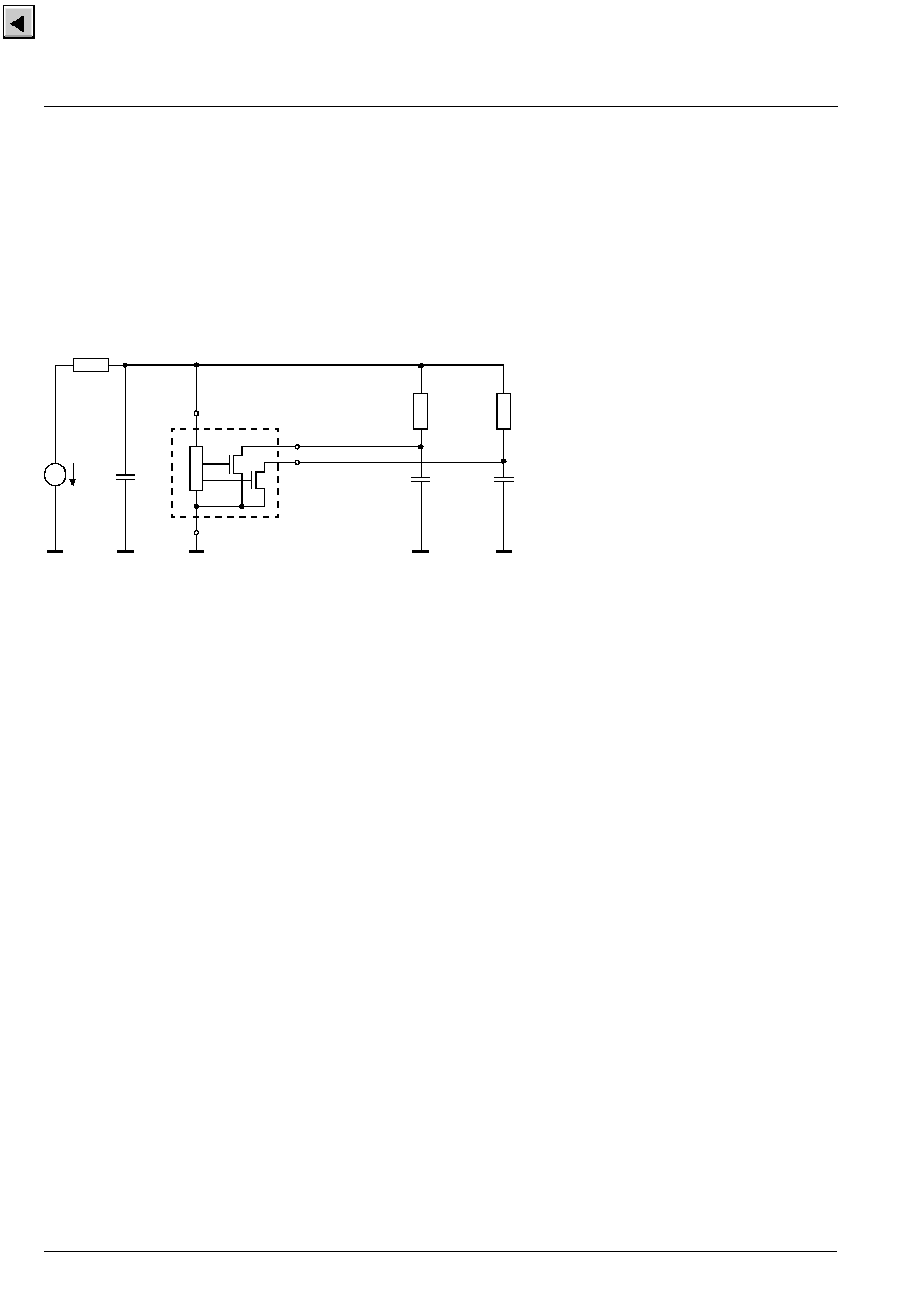
4.6. EMC and ESD
For applications that cause disturbances on the supply
line or radiated disturbances, a series resistor and a
capacitor are recommended (see Fig. 4≠1). The series
resistor and the capacitor should be placed as closely
as possible to the Hall sensor.
Please contact Micronas for detailed investigation
reports with EMC and ESD results.
Fig. 4≠1: Test circuit for EMC investigations
5. Data Sheet History
1. Advance Information: "HAL710 Hall-Effect Sensor
with Direction Detection", Feb. 20, 2001,
6251-478-1AI. First release of the advance informa-
tion.
1 V
DD
4
GND
3 Count Output
2 Direction Output
R
V
220
V
EMC
V
P
4.7 nF
R
L
2.4 k
20 pF
R
L
2.4 k
20 pF