 | –≠–ª–µ–∫—Ç—Ä–æ–Ω–Ω—ã–π –∫–æ–º–ø–æ–Ω–µ–Ω—Ç: HBFP0405 | –°–∫–∞—á–∞—Ç—å:  PDF PDF  ZIP ZIP |

High Performance Isolated
Collector Silicon Bipolar
Transistor
Technical Data
Features
∑ Ideal for High Gain, Low
Current Applications
∑ Typical Performance at
1.8 GHz
Associated Gain of 18 dB
and Noise Figure of 1.2 dB
at 2 V and 2 mA
P
1dB
of 5 dBm at 2 V and
5 mA
∑ Miniature 4-lead SC-70
(SOT-343) Plastic Package
∑ Transition Frequency
f
T
= 25 GHz
Applications
∑ LNA, Oscillator, Driver
Amplifier, Buffer Amplifier,
and Down Converter for
Cellular and PCS Handsets
and Cordless Telephones
∑ Oscillator for TV Delivery
and TVRO Systems up to
12 GHz
HBFP-0405
Description
Hewlett Packard's HBFP-0405 is a
high performance isolated
collector silicon bipolar junction
transistor housed in a 4-lead SC-70
(SOT-343) surface mount plastic
package.
HBFP-0405 provides an associated
gain of 18 dB, noise figure of
1.2 dB, and P
1dB
of 5 dBm at
1.8 GHz. Because of high gain and
low current characteristics,
HBFP-0405 is ideal for cellular/
PCS
as well as for C-Band and
Ku-Band
applications.
This product is based on a 25 GHz
transition frequency fabrication
process, which enables the
products to be used for high
performance, low noise applica-
tions at 900 MHz, 1.9 GHz,
2.4 GHz, and beyond.
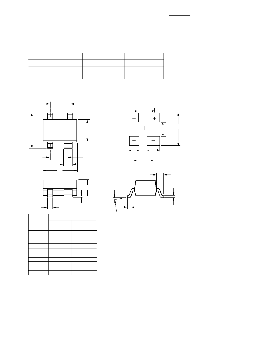
Surface Mount Plastic
Package/ SOT-343 (SC-70)
Outline 4T
Pin Configuration
Collector
Emitter
Base
02
Emitter
Note:
Package marking provides orientation
and identification.
2
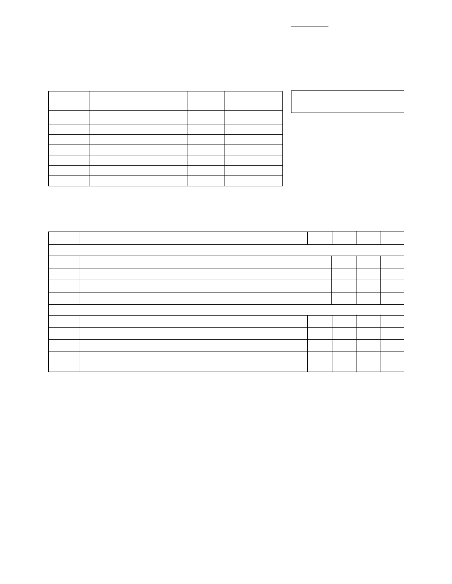
HBFP-0405 Absolute Maximum Ratings
Absolute
Symbol
Parameter
Units
Maximum
[1]
V
EBO
Emitter-Base Voltage
V
1.5
V
CBO
Collector-Base Voltage
V
15.0
V
CEO
Collector-Emitter Voltage
V
4.5
I
C
Collector Current
mA
12
P
T
Power Dissipation
[2]
mW
54
T
j
Junction Temperature
∞
C
150
T
STG
Storage Temperature
∞
C
-65 to 150
Thermal Resistance:
jc
= 550
∞
C/W
Notes:
1. Permanent damage may occur if
any of these limits are exceeded.
2. P
T
limited by maximum ratings.
Electrical Specifications, T
C
= 25
∞
C
Symbol
Parameters and Test Conditions
Units Min.
Typ. Max.
DC Characteristics
BV
CEO
Collector-Emitter Breakdown Voltage
I
C
= 1 mA, open base
V
4.5
I
CBO
Collector-Cutoff Current
V
CB
= 5 V, I
E
= 0
nA
150
I
EBO
Emitter-Base Cutoff Current
V
EB
= 1.5 V, I
C
= 0
µ
A
15
h
FE
DC Current Gain
V
CE
= 2 V, I
C
= 2 mA
--
50
80
150
RF Characteristics
F
MIN
Minimum Noise Figure
I
C
= 2 mA, V
CE
= 2 V, f = 1.8 GHz
dB
1.2
1.5
G
a
Associated Gain
I
C
= 2 mA, V
CE
= 2 V, f = 1.8 GHz
dB
16.5
18
|S
21
|
2
Insertion Power Gain
I
C
= 5 mA, V
CE
= 2 V, f = 1.8 GHz
dB
17
P
-1 dB
Power Output @ 1 dB
I
C
= 5 mA, V
CE
= 2 V, f = 1.8 GHz dBm
5
Compression Point
3
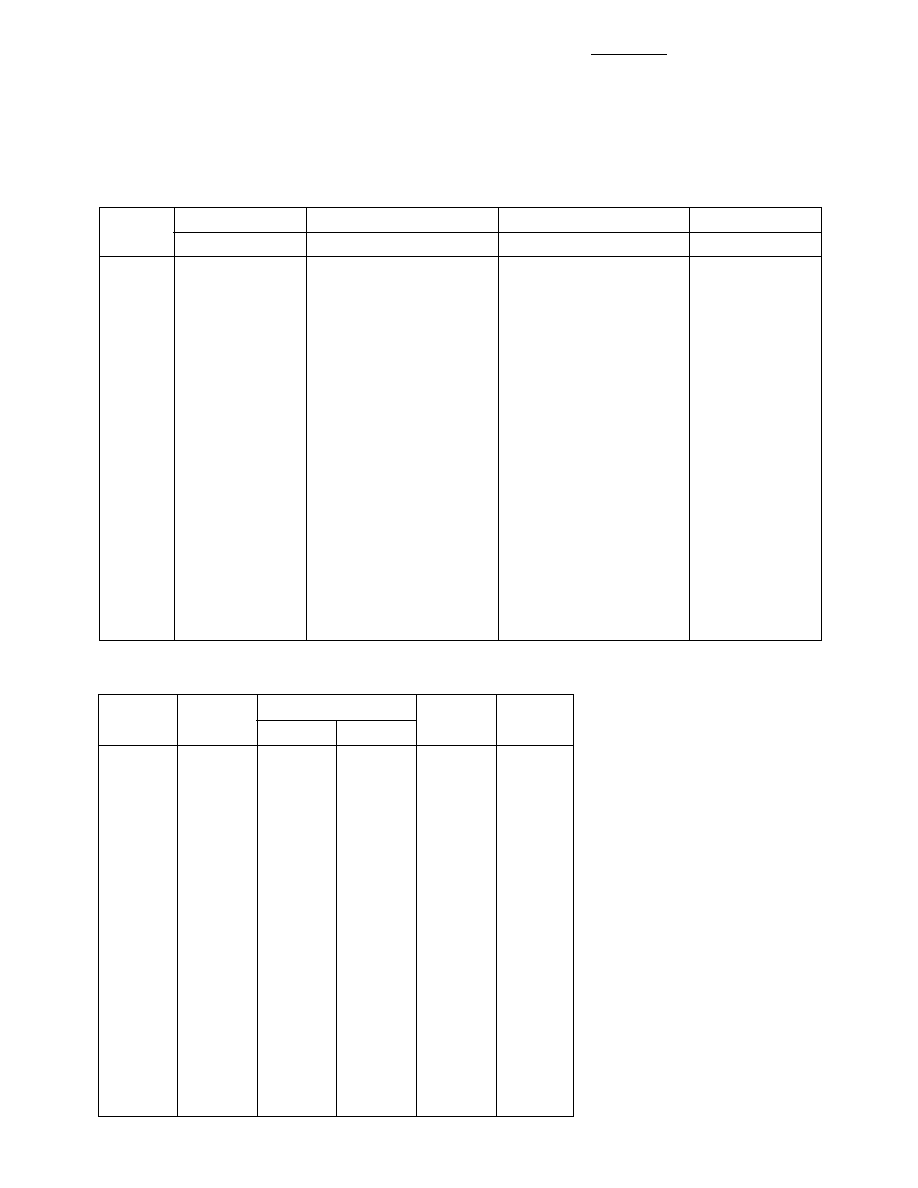
HBFP-0405 Typical Scattering Parameters,
V
CE
= 2 V, I
C
= 2 mA, T
C
= 25
∞
C
Freq.
S
11
S
21
S
12
S
22
GHz
Mag
Ang
dB
Mag
Ang
dB
Mag
Ang
Mag
Ang
0.1
0.910
-4.2
16.5
6.665
176.2
-49.6
0.003
88.5
0.995
-2.2
0.5
0.889
-21.2
16.3
6.496
160.6
-35.6
0.017
80.5
0.982
-10.5
0.9
0.855
-37.6
15.7
6.101
146.0
-30.4
0.030
71.9
0.951
-18.8
1.0
0.841
-41.4
15.6
5.993
142.5
-29.5
0.033
69.6
0.937
-20.9
1.5
0.774
-60.9
14.8
5.484
125.9
-26.4
0.048
57.5
0.880
-30.8
1.8
0.730
-72.0
14.3
5.164
116.8
-25.1
0.055
50.6
0.843
-36.4
2.0
0.701
-79.4
13.9
4.964
110.9
-24.5
0.059
46.4
0.817
-39.8
2.5
0.634
-96.0
13.0
4.450
97.0
-23.4
0.068
37.0
0.758
-47.8
3.0
0.570
-112.3
12.0
3.996
84.7
-22.7
0.073
28.7
0.708
-54.9
3.5
0.521
-127.0
11.2
3.620
73.4
-22.3
0.077
21.7
0.669
-60.9
4.0
0.477
-141.2
10.4
3.320
62.9
-21.9
0.080
15.6
0.634
-66.4
4.5
0.443
-154.7
9.7
3.047
53.6
-21.8
0.082
10.7
0.613
-71.5
5.0
0.412
-168.7
9.0
2.829
44.2
-21.5
0.084
6.0
0.591
-76.4
5.5
0.386
177.1
8.5
2.646
34.9
-21.3
0.087
1.6
0.571
-80.8
6.0
0.372
162.2
7.9
2.493
25.6
-21.0
0.089
-2.1
0.550
-86.1
6.5
0.369
147.7
7.5
2.371
16.8
-20.7
0.093
-7.0
0.525
-90.5
7.0
0.366
130.7
7.1
2.258
8.1
-20.4
0.096
-10.7
0.496
-95.2
7.5
0.370
116.2
6.6
2.141
-1.3
-20.0
0.100
-14.7
0.471
-100.2
8.0
0.387
102.9
6.2
2.042
-9.8
-19.8
0.103
-19.2
0.444
-106.7
8.5
0.405
91.4
5.7
1.937
-18.3
-19.5
0.105
-23.6
0.425
-113.9
9.0
0.421
80.9
5.3
1.834
-26.6
-19.3
0.109
-27.9
0.411
-121.3
9.5
0.437
70.5
4.9
1.753
-35.2
-19.0
0.112
-32.4
0.398
-127.7
10.0
0.454
60.3
4.4
1.669
-43.7
-18.8
0.115
-37.0
0.385
-133.5
HBFP-0405 Noise Parameters:
V
CE
= 2 V, I
C
= 2 mA
Freq.
F
min
opt
R
N
/50
G
a
GHz
dB
Mag
Ang
dB
0.9
1.07
0.569
9.3
20.9
23.46
1.0
1.09
0.558
11.6
20.6
22.67
1.5
1.19
0.504
22.0
19.2
19.64
1.8
1.25
0.474
28.7
18.5
18.28
2.0
1.29
0.456
33.6
18.0
17.50
2.5
1.39
0.423
48.2
16.6
15.91
3.0
1.48
0.391
59.3
15.6
14.39
3.5
1.57
0.352
72.1
14.2
13.29
4.0
1.70
0.318
83.1
13.0
12.29
4.5
1.78
0.290
93.9
12.1
11.43
5.0
1.87
0.257
107.3
10.9
10.71
5.5
2.00
0.215
118.3
10.5
10.03
6.0
2.10
0.179
133.7
10.4
9.47
6.5
2.18
0.157
153.1
10.2
8.97
7.0
2.29
0.125
-179.2
11.0
8.50
7.5
2.35
0.116
-154.8
12.0
7.98
8.0
2.50
0.140
-123.4
13.7
7.63
8.5
2.65
0.163
-104.1
15.9
7.21
9.0
2.76
0.191
-89.2
18.6
6.81
9.5
2.93
0.226
-73.4
22.3
6.51
10.0
2.94
0.254
-61.4
26.3
6.16
S and noise parameters are measured
on a microstrip line made on
0.025 inch thick alumina carrier. The
input reference plane is at the end of
the base lead, the output reference
plane is at the end of the collector
lead. S and noise parameters include
the effect of four plated through via
holes connecting emitter landing pads
on the top of test carrier to the
microstrip ground plane on the
bottom side of the carrier. Two
0.020 inch diameter via holes are
placed within 0.010 inch from each
emitter lead contact point, one via on
each side of that point.
4
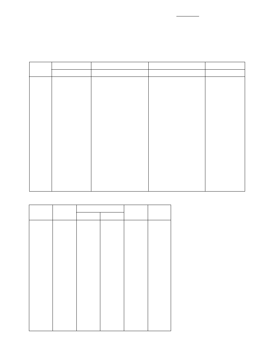
HBFP-0405 Typical Scattering Parameters,
V
CE
= 2 V, I
C
= 5 mA, T
C
= 25
∞
C
Freq.
S
11
S
21
S
12
S
22
GHz
Mag
Ang
dB
Mag
Ang
dB
Mag
Ang
Mag
Ang
0.1
0.819
-6.2
22.0
12.630
174.5
-50.2
0.003
87.8
0.990
-2.8
0.5
0.775
-30.3
21.5
11.912
153.5
-36.2
0.016
77.1
0.959
-13.4
0.9
0.704
-52.4
20.6
10.664
134.9
-31.5
0.027
67.3
0.897
-23.3
1.0
0.681
-57.2
20.3
10.308
130.7
-30.8
0.029
64.9
0.875
-25.5
1.5
0.585
-81.5
18.8
8.689
111.9
-28.1
0.039
54.0
0.783
-35.2
1.8
0.531
-94.5
17.9
7.817
102.5
-27.2
0.044
49.0
0.733
-40.1
2.0
0.500
-102.7
17.3
7.306
96.7
-26.6
0.047
46.0
0.703
-43.0
2.5
0.440
-121.3
15.9
6.208
83.7
-25.6
0.053
39.9
0.641
-49.4
3.0
0.392
-138.9
14.6
5.362
72.4
-24.8
0.057
34.6
0.597
-55.0
3.5
0.360
-154.1
13.5
4.716
62.3
-24.2
0.061
30.4
0.566
-59.7
4.0
0.334
-168.9
12.5
4.214
52.9
-23.6
0.066
26.5
0.541
-64.2
4.5
0.315
177.0
11.6
3.814
44.3
-23.1
0.070
23.0
0.528
-68.6
5.0
0.302
162.5
10.9
3.491
35.7
-22.5
0.075
19.0
0.513
-73.0
5.5
0.295
148.1
10.2
3.229
27.4
-22.0
0.079
15.1
0.499
-77.0
6.0
0.301
133.7
9.6
3.010
19.0
-21.5
0.084
11.1
0.484
-82.0
6.5
0.311
120.4
9.0
2.827
10.8
-21.0
0.089
6.4
0.463
-86.1
7.0
0.327
105.9
8.5
2.668
2.6
-20.5
0.095
2.1
0.439
-90.5
7.5
0.346
94.0
8.0
2.520
-5.8
-20.0
0.101
-3.0
0.414
-95.4
8.0
0.369
83.4
7.6
2.389
-13.8
-19.5
0.106
-7.7
0.389
-101.6
8.5
0.392
74.1
7.1
2.261
-21.9
-19.1
0.110
-12.8
0.370
-108.5
9.0
0.410
65.6
6.6
2.141
-29.9
-18.7
0.116
-18.0
0.357
-115.8
9.5
0.428
56.9
6.2
2.038
-38.0
-18.4
0.120
-23.1
0.345
-122.3
10.0
0.446
48.2
5.7
1.937
-46.0
-18.1
0.124
-28.5
0.334
-127.9
HBFP-0405 Noise Parameters:
V
CE
= 2 V, I
C
= 5 mA
Freq.
F
min
opt
R
N
/50
G
a
GHz
dB
Mag
Ang
dB
0.9
1.36
0.386
2.8
17.0
25.59
1.0
1.38
0.375
5.0
16.8
24.76
1.5
1.46
0.333
17.7
16.2
21.56
1.8
1.52
0.305
25.5
15.6
20.12
2.0
1.55
0.292
31.9
15.3
19.29
2.5
1.65
0.246
50.0
13.8
17.61
3.0
1.73
0.208
59.9
13.1
16.04
3.5
1.79
0.187
73.6
12.6
14.81
4.0
1.93
0.153
85.6
12.0
13.76
4.5
1.99
0.123
100.2
11.8
12.90
5.0
2.08
0.104
119.5
11.3
12.12
5.5
2.18
0.065
141.5
12.0
11.45
6.0
2.32
0.051
-169.0
12.7
10.87
6.5
2.37
0.068
-129.9
13.5
10.32
7.0
2.48
0.101
-96.3
15.2
9.82
7.5
2.56
0.133
-82.9
17.0
9.33
8.0
2.69
0.177
-71.2
19.7
8.92
8.5
2.85
0.212
-62.8
22.8
8.50
9.0
2.99
0.246
-54.1
26.7
8.10
9.5
3.10
0.282
-46.1
30.9
7.77
10.0
3.12
0.314
-37.3
35.2
7.41
S and noise parameters are measured
on a microstrip line made on
0.025 inch thick alumina carrier. The
input reference plane is at the end of
the base lead, the output reference
plane is at the end of the collector
lead. S and noise parameters include
the effect of four plated through via
holes connecting emitter landing pads
on the top of test carrier to the
microstrip ground plane on the
bottom side of the carrier. Two
0.020 inch diameter via holes are
placed within 0.010 inch from each
emitter lead contact point, one via on
each side of that point.

5
HBFP-0405 Typical Performance
0
5
10
15
30
20
25
0
2
4
8
6
10
ASSOCIATED GAIN
(dB)
FREQUENCY (GHz)
Figure 1. Associated Gain vs.
Frequency and Collector Current
at 2 V.
5
0
10
20
15
30
25
0
2
4
8 10
6
22
ASSOCIATED GAIN
(dB)
COLLECTOR CURRENT (mA)
Figure 2. Noise Figure vs.
Frequency and Collector Current
at V
CE
= 2 V.
Figure 3. Associated Gain vs.
Collector Current and Frequency
at 2 V.
Figure 5. Associated Gain vs. Voltage
and Frequency at 2 mA.
Figure 6. Noise Figure vs. Voltage
and Frequency at 2 mA.
Figure 4. Noise Figure vs. Collector
Current and Frequency at 2 V.
2 mA
5 mA
10 mA
15 mA
12 14
18 20
16
0
0.50
1.00
3.50
3.00
1.50
2.00
0
2
4
6
8
12
14
10
16
NOISE FIGURE
(dB)
COLLECTOR CURRENT (mA)
2.50
0
1
2
4
5
3
6
VOLTAGE (V)
VOLTAGE (V)
0
1
2
3
5
4
0
2
4
8
6
10
NOISE FIGURE
(dB)
FREQUENCY (GHz)
2 mA
5 mA
10 mA
15 mA
0.9 GHz
1.8 GHz
2.5 GHz
3 GHz
4 GHz
5 GHz
6 GHz
0.9 GHz
1.8 GHz
2.5 GHz
3 GHz
4 GHz
5 GHz
6 GHz
5
0
10
20
15
30
25
ASSOCIATED GAIN
(dB)
0.9 GHz
1.8 GHz
2.5 GHz
3 GHz
4 GHz
5 GHz
6 GHz
0
1
2
4
5
3
6
0.50
0
1.00
2.00
1.50
2.50
NOISE FIGURE
(dB)
0.9 GHz
1.8 GHz
2.5 GHz
3 GHz
4 GHz
5 GHz
6 GHz
6
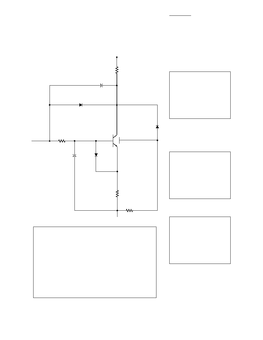
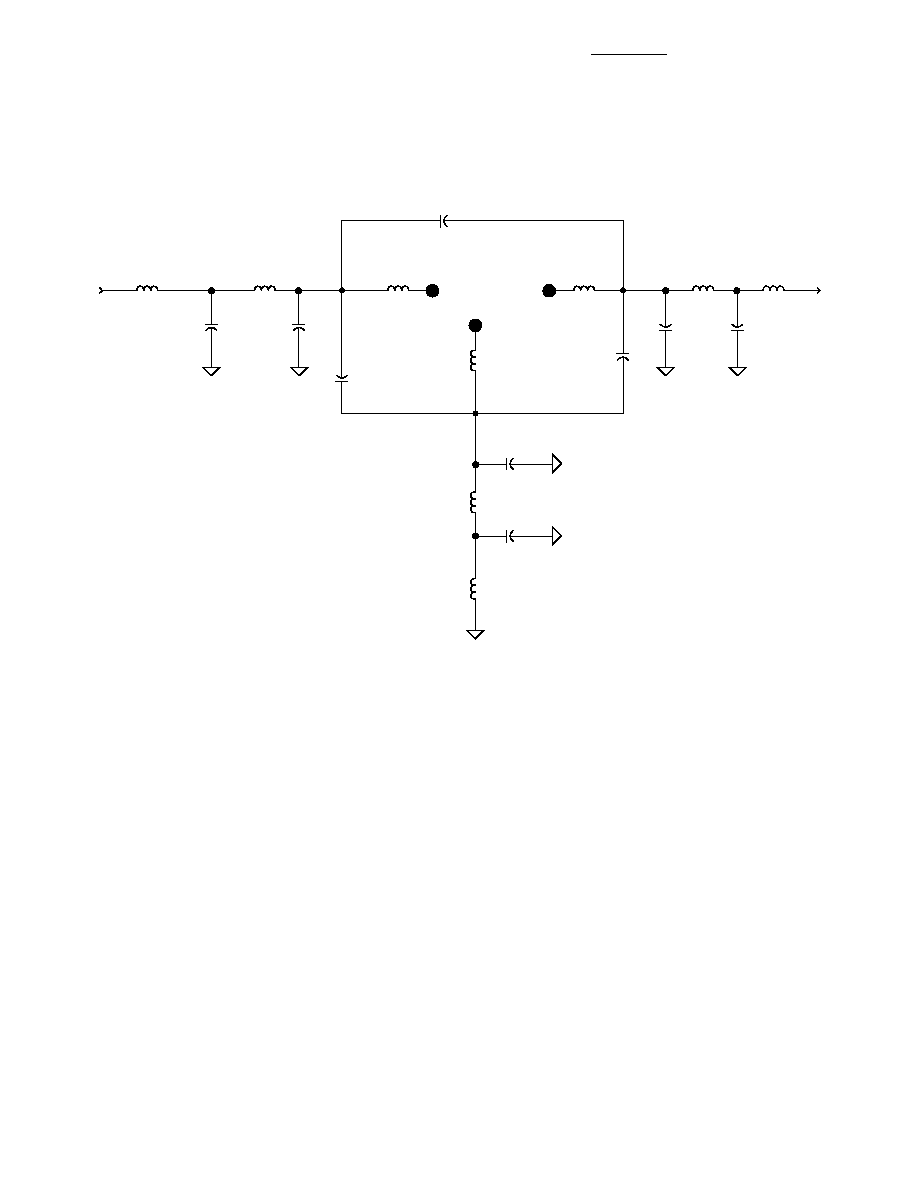
HBFP-0405 Die Model and PSPICE Parameters
CMP9
R
CMP7
R
CMP8
R
CMP69
R
R-1 OH
R=1.565 OH
R=3.74196 OH
R = 6.5915 OH
TEMP=
MODEL=DBE
REGION=
AREA=
AREA=
REGION=
MODEL=BJTMODEL
AREA=
REGION=
MODEL=DCS
TEMP=
AREA=
REGION=
MODEL = DBC
TEMP=
C = 6.227E-3 pF
C = 17.213E-3 pF
XX
CMP1
NPNBJTSUBST
CMP5
C
C
CMP6
C
CMP2
DIODE
CMP16
DIODE
CMP3
DIODE
B
E
IS=IE-24
BV=
IBV=
IMAX=
XTI=
TNOM=21
KF=
AF=
ISR=
NR=
IKF=
NBV=
IBVL=
NBVL=
FFE=
RS=
CJO=2.593E-14
TT=
EG=
VJ=0.8971
M=2.292E-1
N=1.0029
FC=0.8
CMP11
DIODEMODELFORM
# DIODE MODEL #
MODEL = DBE
IS=I.40507E-17
BV=
IBV=
IMAX=
XTI=
TNOM=21
KF=
AF=
ISR=
NR=
IKF=
NBV=
IBVL=
NBVL=
FFE=
RS=
CJO=2.393E-14
TT=
EG=
VJ=0.729
M=0.44
N=1
FC=0.8
CMP10
DIODEMODELFORM
# DIODE MODEL #
MODEL = DBC
IS=IE-24
BV=
IBV=
IMAX=
XTI=
TNOM=21
KF=
AF=
ISR=
NR=
IKF=
NBV=
IBVL=
NBVL=
FFE=
RS=2.17347E2
CJO=8.974E-14
TT=
EG=
VJ=0.6
M=0.42
N=
FC=0.8
CMP12
DIODEMODELFORM
# DIODE MODEL #
MODEL = DCS
NPN=yes
PNP=
VTF=0.8
ITF=2.21805486E-1
PTF=22
XTB=0.7
APPROXOB=yes
Forward
BF=1E6
IKE=1.4737E-1
ISE=7.094E-20
NE=1.006
VAF=4.4E1
NF=1
TF=5.3706E-12
XTF=20
Reverse
BR=1
IKR=1.1E-2
ISC=
NC=2
VAR=3.37
NR=1.005
TR=4E-9
Noise
KI=
AF=
KB=
AB=
FB=
D i o d e a n d j u n c t i o n
EG=1.17
IS=4.4746E-18
IMAX=
XTI=3
TNOM=21
Substrate
IS5=
NS=
P a r a s i t i c s
RB-9.30144818
IRB=3.029562E-6
RBM=.1
RE=
RC=
Substrate
IS5=
NS=
CJC=2.7056E-14
VJC=.6775
MJC=0.3319
FC=0.8
CJE=7.474248E-14
VJE=0.9907
MJE=0.5063
CJS=
VJS=
MJS=
CMP68
BITMODELFORM
# BJT MODEL #
MODEL = BJTMODEL
XCJC=4.39790997E-1
This model can be used as a design tool. It has been tested on MDS for various specifications. However, for more
precise and accurate design, please refer to the measured data in this data sheet.
Note:
The value of beta was high (BF = 1E6) to compensate for the fact that diode DBE reduces the current going into the
base (current flows through DBE). The diodes are necessary to model the non-linear effects.
7
SOT343 Package Model
L = 0.2 nH
L = 0.7 nH
L = 0.2 nH
L = 0.15 nH
L = 0.22 nH
LLB
L
LT1
L
LLI
L
LL2
L
C2T1
C
C1T1
C
CCEB
C
C = 0.08 pF
AGROUND
AGROUND
BASE
COLLECTOR
EMITTER
C = 0.05 pF
C = 0.04 pF
C = 0.04 pF
L = 0.7 nH
CMP44
L
AGROUND
AGROUND
LLE
L
L = 0.1 nH
LT2
L
C2T2
C
C = 0.1 pF
AGROUND
C1T2
C
L = 0.5 nH
L = 0.2 nH
LL3
L
LT3
L
C1T3
C
CCEC
C
C2T3
C
C = 0.1 pF
C = 0.01 pF
AGROUND
AGROUND
C = 0.144 pF
C = 0.05 pF
CCBC
C
8
Package Dimensions
SOT-343 (SC-70 4 Lead)
Part Number Ordering Information
Part Number
Devices per Reel
Container
HBFP-0405-TR1
3000
7" Reel
HBFP-0405-TR2
10,000
13" Reel
HBFP-0405-BLK
100
antistatic bag
E
D
A
A1
b TYP
e
E1
1.30 (0.051)
BSC
1.15 (.045) BSC
h
C TYP
L
DIMENSIONS ARE IN MILLIMETERS (INCHES)
DIMENSIONS
MIN.
0.80 (0.031)
0 (0)
0.25 (0.010)
0.10 (0.004)
1.90 (0.075)
2.00 (0.079)
0.55 (0.022)
0.450 TYP (0.018)
1.15 (0.045)
0.10 (0.004)
0
MAX.
1.00 (0.039)
0.10 (0.004)
0.35 (0.014)
0.20 (0.008)
2.10 (0.083)
2.20 (0.087)
0.65 (0.025)
1.35 (0.053)
0.35 (0.014)
10
SYMBOL
A
A1
b
C
D
E
e
h
E1
L
1.15 (.045) REF
1.30 (.051) REF
1.30 (.051)
2.60 (.102)
0.55 (.021) TYP
0.85 (.033)
9
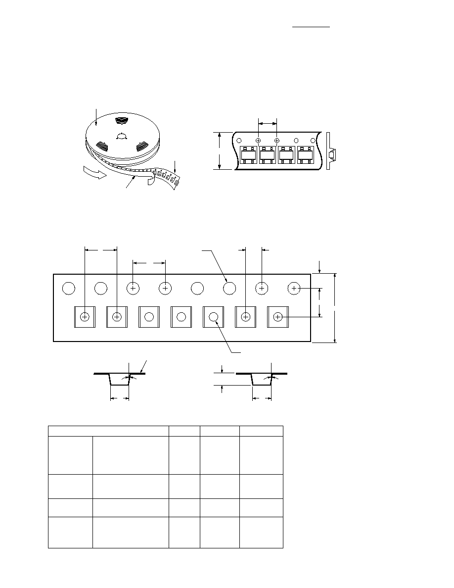
Device Orientation
Tape Dimensions
For Outline 4T
USER
FEED
DIRECTION
COVER TAPE
CARRIER
TAPE
REEL
END VIEW
8 mm
4 mm
TOP VIEW
P
P
0
P
2
F
W
D
1
D
E
A
0
8
∞
MAX.
t
1
(CARRIER TAPE THICKNESS)
5
∞
MAX.
B
0
K
0
DESCRIPTION
SYMBOL
SIZE (mm)
SIZE (INCHES)
LENGTH
WIDTH
DEPTH
PITCH
BOTTOM HOLE DIAMETER
A
0
B
0
K
0
P
D
1
2.24
±
0.10
2.34
±
0.10
1.22
±
0.10
4.00
±
0.10
1.00 + 0.25
0.088
±
0.004
0.092
±
0.004
0.048
±
0.004
0.157
±
0.004
0.039 + 0.010
CAVITY
DIAMETER
PITCH
POSITION
D
P
0
E
1.55
±
0.05
4.00
±
0.10
1.75
±
0.10
0.061
±
0.002
0.157
±
0.004
0.069
±
0.004
PERFORATION
WIDTH
THICKNESS
W
t
1
8.00
±
0.30
0.255
±
0.013
0.315
±
0.012
0.010
±
0.0005
CARRIER TAPE
CAVITY TO PERFORATION
(WIDTH DIRECTION)
CAVITY TO PERFORATION
(LENGTH DIRECTION)
F
P
2
3.50
±
0.05
2.00
±
0.05
0.138
±
0.002
0.079
±
0.002
DISTANCE
02
02
02
02

www.hp.com/go/rf
For technical assistance or the location of
your nearest Hewlett-Packard sales
office, distributor or representative call:
Americas/Canada:
1-800-235-0312 or
408-654-8675
Far East/Australasia:
Call your local HP
sales office.
Japan:
(81 3) 3335-8152
Europe:
Call your local HP sales office.
Data subject to change.
Copyright © 1998 Hewlett-Packard Co.
Printed in U.S.A.
5968-0140E (6/98)