 | –≠–ª–µ–∫—Ç—Ä–æ–Ω–Ω—ã–π –∫–æ–º–ø–æ–Ω–µ–Ω—Ç: HCC4017BF | –°–∫–∞—á–∞—Ç—å:  PDF PDF  ZIP ZIP |
HCC/HCF4017B
HCC/HCF4022B
COUNTERS/DIVIDERS
.
FULLY STATIC OPERATION
.
MEDIUM SPEED OPERATION-12MHz (typ.) AT
V
DD
= 10V
.
STANDARDIZED
SYMMETRICAL
OUTPUT
CHARACTERISTICS
.
QUIESCENT CURRENT SPECIFIED TO 20V
FOR HCC DEVICE
.
INPUT CURRENT OF 100nA AT 18V AND 25
∞
C
FOR HCC DEVICE
.
100% TESTED FOR QUIESCENT CURRENT
.
5V, 10V, AND 15V PARAMETRIC RATINGS
.
MEETS ALL REQUIREMENTS OF JEDEC TEN-
TATIVE STANDARD N
∞
13A, "STANDARD
SPECIFICATIONS FOR DESCRIPTION OF "B"
SERIES CMOS DEVICES"
June 1989
EY
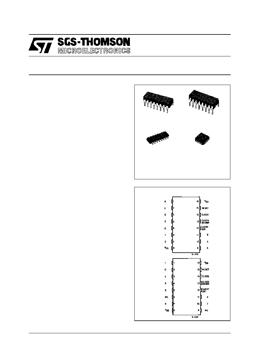
(Plastic Package)
F
(Ceramic Frit Seal Package)
C1
(Plastic Chip Carrier)
ORDER CODES :
HCC40XXBF
HCF40XXBM1
HCF40XXBEY
HCF40XXBC1
PIN CONNECTIONS
4017B DECADE COUNTER WITH 10
DECODED OUTPUTS
4022B OCTAL COUNTER WITH 8
DECODED OUTPUTS
4017B
4022B
M1
(Micro Package)
DESCRIPTION
The HCC4017B/4022B (extended temperature
range) and HCF4017B/4022B (intermediate tem-
perature range) are monolithic integrated circuits,
available in 16-lead dual in-line plastic or ceramic
package and plastic micro package.
The HCC/HCF4017B and HCC/HCF4022B are 5-
stage and 4-stage Johnson counters having 10 and
8 decoded outputs, respectively. Inputs include a
CLOCK, a RESET, and a CLOCK INHIBIT signal.
Schmitt trigger action in the CLOCK input circuit pro-
vides pulse shaping that allows unlimited clock input
pulse rise and fall times. These counters are ad-
vanced one count at the positive clock signal tran-
sition if the CLOCK INHIBIT signal is low. Counter
advancement via the clock line is inhibited when the
CLOCK INHIBIT signal is high. A high RESET signal
clears the counter to its zero count. Use of the
Johnson decade-counter
configuration permits
high-speed operation, 2-input decimal-decode gat-
ing, and spike-free decoded outputs. Anti-lock gat-
ing is provided, thus assuring proper counting
sequence. The decoded outputs are normally low
and go high only at their respective decoded time
slot. Each decoded output remains high for one full
clock cycle. A CARRY-OUT signal completes one
1/12
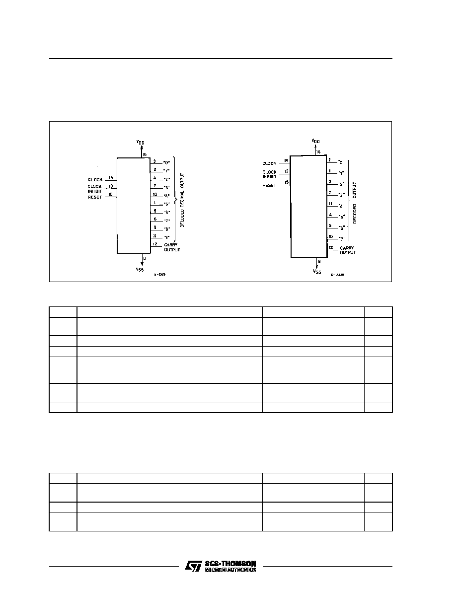
FUNCTIONAL DIAGRAM
ABSOLUTE MAXIMUM RATINGS
Symbol
Parameter
Value
Unit
V
DD
*
Supply Voltage : HCC Types
HC F Types
≠ 0.5 to + 20
≠ 0.5 to + 18
V
V
V
I
Input Voltage
≠ 0.5 to V
DD
+ 0.5
V
I
I
DC Input Current (any one input)
±
10
mA
P
t o t
Total Power Dissipation (per package)
Dissipation per Output Transistor
for T
o p
= Full Package-temperature Range
200
100
mW
mW
T
o p
Operating Temperature : HCC Types
H CF Types
≠ 55 to + 125
≠ 40 to + 85
∞
C
∞
C
T
s t g
Storage Temperature
≠ 65 to + 150
∞
C
RECOMMENDED OPERATING CONDITIONS
Symbol
Parameter
Value
Unit
V
DD
Supply Voltage : HCC Types
HC F Types
3 to 18
3 to 15
V
V
V
I
Input Voltage
0 to V
DD
V
T
o p
Operating Temperature : HCC Types
H CF Types
≠ 55 to + 125
≠ 40 to + 85
∞
C
∞
C
4022B
Stresses above those listed under "Absolute Maximum Ratings" may cause permanent damage to the device. This is a stress
rating only and functional operation of the device at these or any other conditions above those indicated in the operational sec-
tions of this specifi cation is not implied. Exposure to absolute maximum rating conditions for external periods may affect device
reliability.
* All voltages values are referred to V
SS
pin voltage.
4017B
cycle
every
10
clock
input
cycles
in
the
HCC/HCF4017B or every 8 clock input cycles in the
HCC/HCF4022B and is used to ripple-clock the suc-
ceeding device in a multi-device counting chain.
HCC/HCF4017B/4022B
2/12
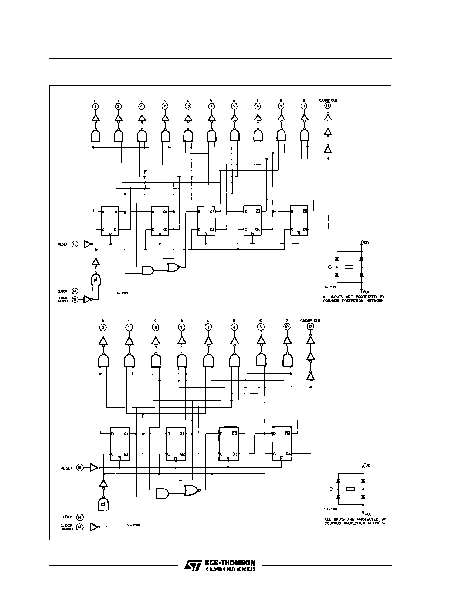
LOGIC DIAGRAMS
4017B
4022
HCC/HCF4017B/4022B
3/12
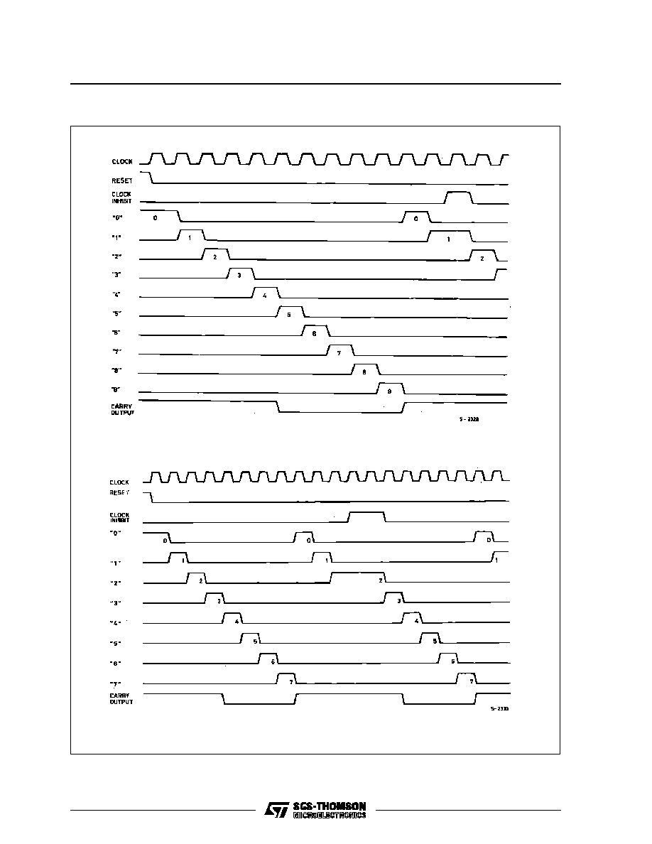
TIMING DIAGRAMS
4017B
4022B
HCC/HCF4017B/4022B
4/12
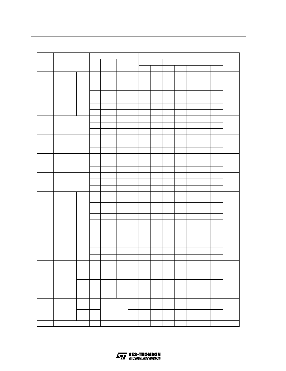
STATIC ELECTRICAL CHARACTERISTICS (over recommended operating conditions)
Test Conditions
Value
V
I
V
O
| I
O
|
V
DD
T
Low
*
25
∞
C
T
High
*
Symbol
Parameter
(V)
(V)
(
µ
A)
(V)
Min.
Max.
Min.
Typ.
Max.
Min.
Max.
Unit
I
L
Quiescent
Current
HCC
Types
0/ 5
5
5
0.04
5
150
µ
A
0/10
10
10
0.04
10
300
0/15
15
20
0.04
20
600
0/20
20
100
0.08
100
3000
HCF
Types
0/ 5
5
20
0.04
20
150
0/10
10
40
0.04
40
300
0/15
15
80
0.04
80
600
V
OH
Output High
Voltage
0/ 5
< 1
5
4.95
4.95
4.95
V
0/10
< 1
10
9.95
9.95
9.95
0/15
< 1
15
14.95
14.95
14.95
V
OL
Output Low
Voltage
5/0
< 1
5
0.05
0.05
0.05
V
10/0
< 1
10
0.05
0.05
0.05
15/0
< 1
15
0.05
0.05
0.05
V
IH
Input High
Voltage
0.5/4.5
< 1
5
3.5
3.5
3.5
V
1/9
< 1
10
7
7
7
1.5/13.5 < 1
15
11
11
11
V
IL
Input Low
Voltage
4.5/0.5
< 1
5
1.5
1.5
1.5
V
9/1
< 1
10
3
3
3
13.5/1.5 < 1
15
4
4
4
I
OH
Output
Drive
Current
HCC
Types
0/ 5
2.5
5
≠ 2
≠ 1.6 ≠ 3.2
≠
1.15
mA
0/ 5
4.6
5
≠
0.64
≠
0.51
≠ 1
≠
0.36
0/10
9.5
10
≠ 1.6
≠ 1.3 ≠ 2.6
≠ 0.9
0/15
13.5
15
≠ 4.2
≠ 3.4 ≠ 6.8
≠ 2.4
HCF
Types
0/ 5
2.5
5
≠
1.53
≠
1.36
≠ 3.2
≠ 1.1
0/ 5
4.6
5
≠
0.52
≠
0.44
≠ 1
≠
0.36
0/10
9.5
10
≠ 1.3
≠ 1.1 ≠ 2.6
≠ 0.9
0/15
13.5
15
≠ 3.6
≠ 3.0 ≠ 6.8
≠ 2.4
I
OL
Output
Sink
Current
HCC
Types
0/ 5
0.4
5
0.64
0.51
1
0.36
mA
0/10
0.5
10
1.6
1.3
2.6
0.9
0/15
1.5
15
4.2
3.4
6.8
2.4
HCF
Types
0/ 5
0.4
5
0.52
0.44
1
0.36
0/10
0.5
10
1.3
1.1
2.6
0.9
0/15
1.5
15
3.6
3.0
6.8
2.4
I
IH
, I
IL
Input
Leakage
Current
HCC
Types
0/18
Any Input
18
±
0.1
±
10
≠5
±
0.1
±
1
µ
A
HCF
Types
0/15
15
±
0.3
±
10
≠5
±
0.3
±
1
C
I
Input Capacitance
Any Input
5
7.5
pF
* T
Lo w
=
≠ 55
∞
C for HCC device : ≠ 40
∞
C for HCF device.
* T
High
=
+ 125
∞
C for HCC device : + 85
∞
C for HCF device.
The Noise Margin for both "1" and "0" level is : 1V min. width
V
DD
= 5V, 2V min. width V
DD
= 10V, 2.5V min. width V
DD
=
15V.
HCC/HCF4017B/4022B
5/12
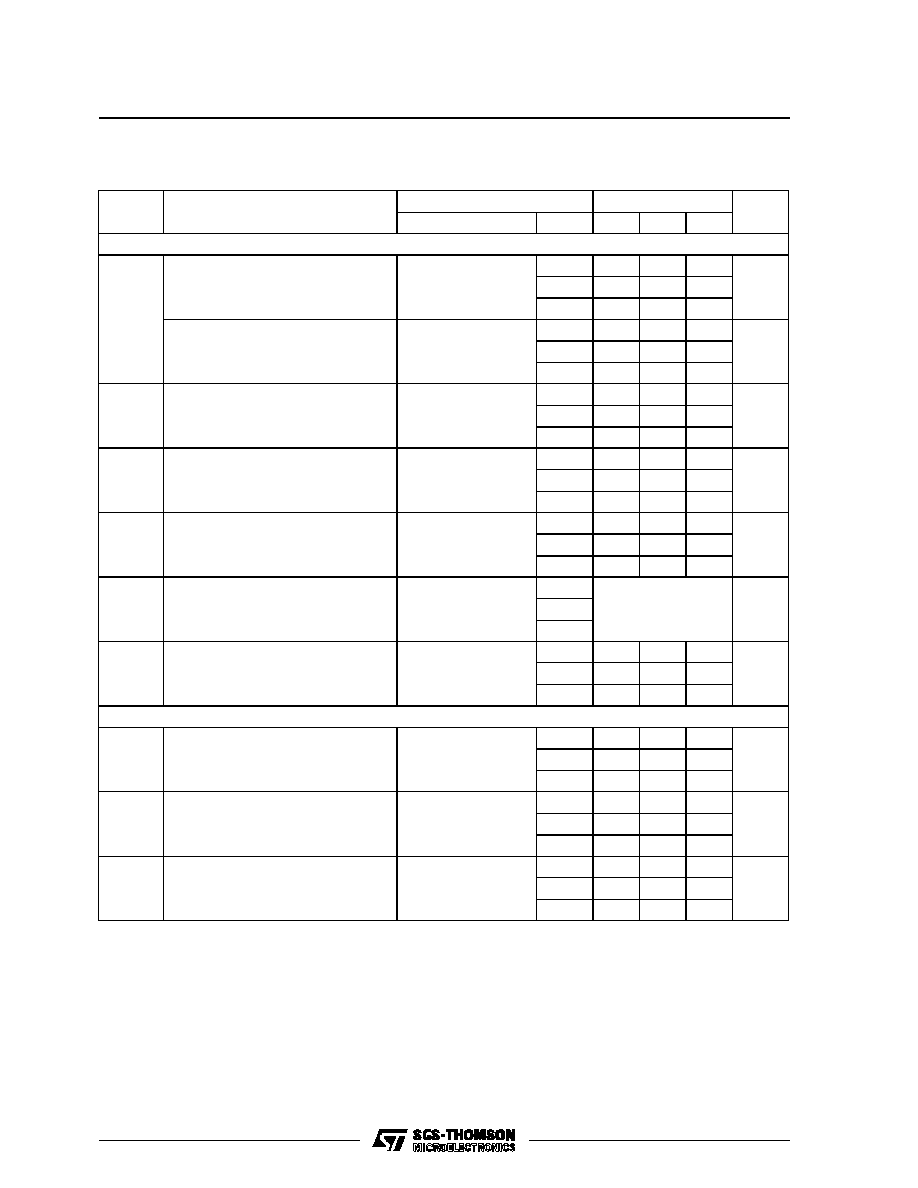
DYNAMIC ELECTRICAL CHARACTERISTICS (T
amb
= 25
∞
C, C
L
= 50pF, R
L
= 200k
,
typical temperature coefficient for all V
DD
= 0.3%/
∞
C values, all input rise and fall time = 20ns)
Value
Symbol
Parameter
Test Conditions
V
DD
(V)
Min.
Typ.
Max.
Unit
CLOCKED OPERATI ON
t
PLH
, t
PHL
Propagation Delay Time
Decode Out
5
325
650
ns
10
135
270
15
85
170
Carry Out
5
300
600
ns
10
125
250
15
80
160
t
THL
, t
TLH
Transition Time
Carry Out or Decoded Out Line
5
100
200
ns
10
50
100
15
40
80
f
CL
*
Maximum Clock Input Frequency
5
2.5
5
5
MHz
10
5
10
15
5.5
11
t
W
Minimum Clock Pulse Width
5
100
200
ns
10
45
90
15
30
60
t
r
, t
f
Clock Input Rise or Fall Time
5
Unlimited
µ
s
10
15
t
set up
Data Setup Time
Minimum Clock Inhibit
5
115
230
ns
10
50
100
15
35
7.5
RESET OPERATI ON
t
PLH
, t
PHL
Propagation Delay Time
Carry Out or Decode Out Lines
5
265
530
ns
10
115
230
15
85
170
t
W
Minimum Reset Pulse Width
5
130
260
ns
10
55
110
15
30
60
t
rem
Minimum Reset Removal Time
5
200
400
ns
10
140
280
15
75
150
* Measured with respect to carry output line.
HCC/HCF4017B/4022B
6/12
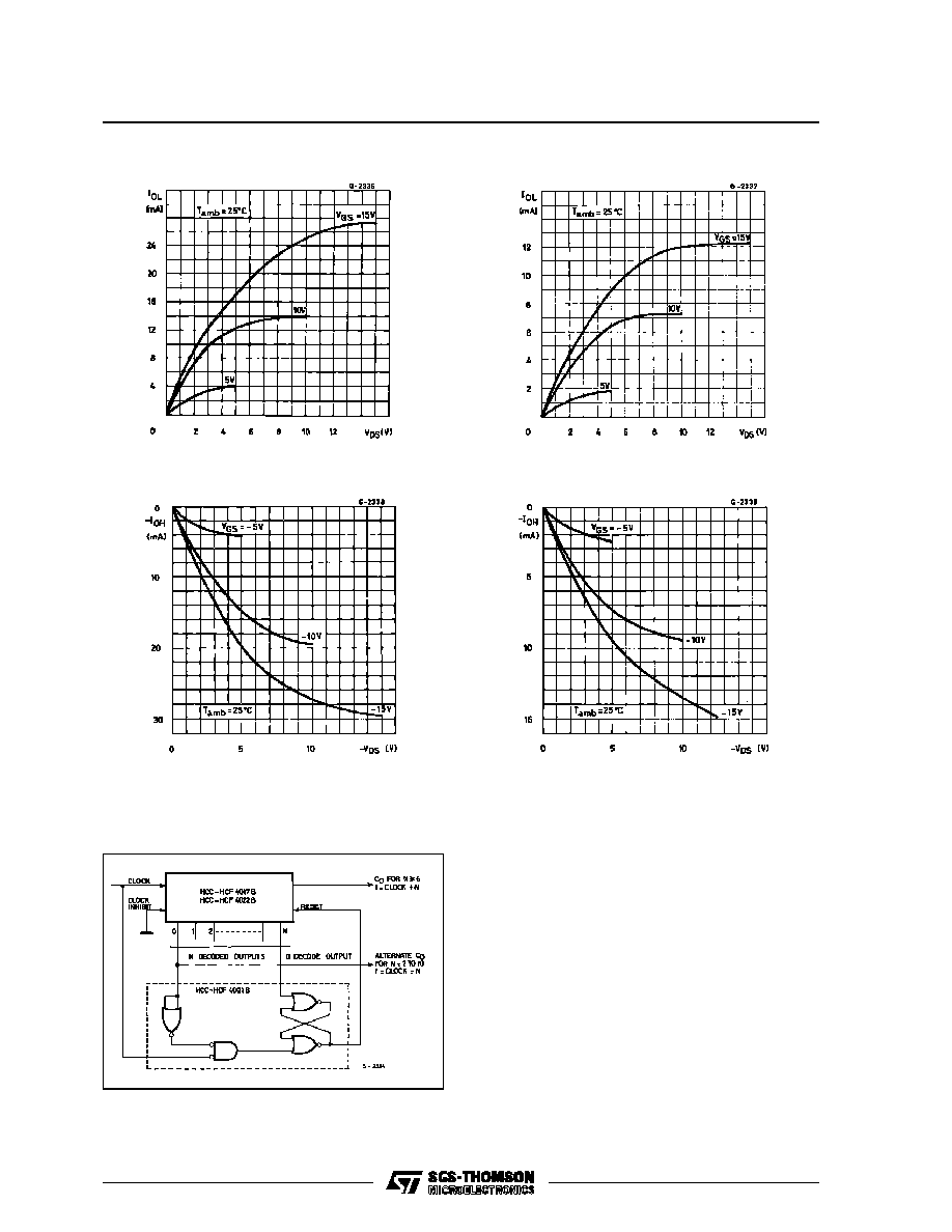
Typical Output Low (sink) Current Characteristics.
Minimum Output Low (sink) Current Characteristics.
Typical
Output High (source) Current Charac-
teristics.
Minimum Output High (source ) Current Charac-
teristics.
TYPICAL APPLICATIONS
Divide by N Counter (N
10) with N Decoded Out-
puts.
When the N
th
decoded output is reached (N
th
clock pulse) the S-R flip-flop (constructed from
two NOR gates of the HCC/HCF4001B) gener-
ates
a
reset
pulse
which
clears
the
HCC/HCF4017B to its zero count. At this time, if
the N
th
decoded output is greater than or equal
to 6, the C
OUT
line goes high to clock the next
HCC/HCF4017B
counter
section.
The
"0"
decoded output also goes high at this time. Coin-
cidence of the clock low and decoded "0" output
high resets the S-R flip flop to enable the
HCC/HCF4017B. If the N
th
decoded output is
less than 6, the C
OUT
line will not go high and,
therefore, cannot be used. In this case "0"
decoded output may be used to perform the
clocking function for the next counter.
HCC/HCF4017B/4022B
7/12
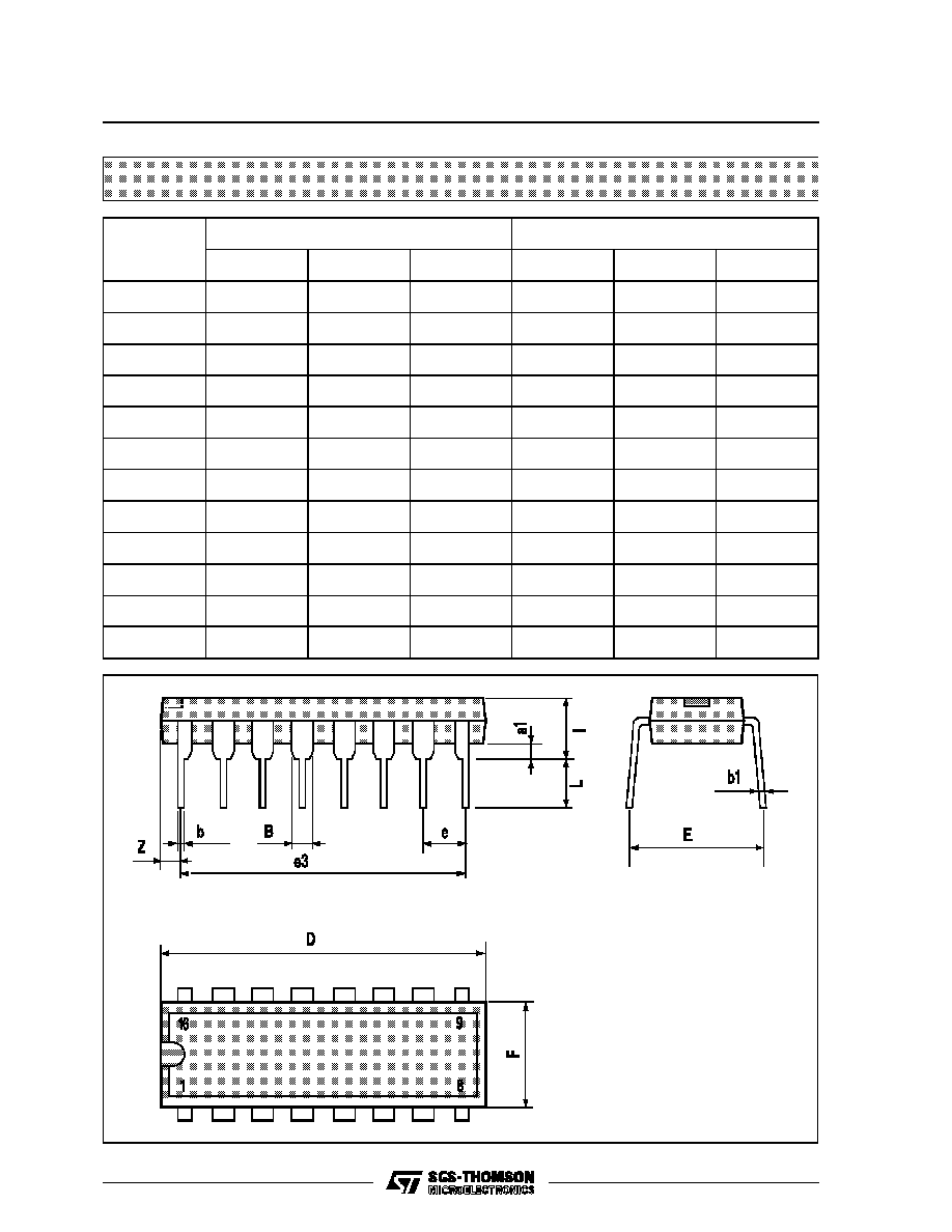
Plastic DIP16 (0.25) MECHANICAL DATA
DIM.
mm
inch
MIN.
TYP.
MAX.
MIN.
TYP.
MAX.
a1
0.51
0.020
B
0.77
1.65
0.030
0.065
b
0.5
0.020
b1
0.25
0.010
D
20
0.787
E
8.5
0.335
e
2.54
0.100
e3
17.78
0.700
F
7.1
0.280
I
5.1
0.201
L
3.3
0.130
Z
1.27
0.050
P001C
HCC/HCF4017B/4022B
8/12

Ceramic DIP16/1 MECHANICAL DATA
DIM.
mm
inch
MIN.
TYP.
MAX.
MIN.
TYP.
MAX.
A
20
0.787
B
7
0.276
D
3.3
0.130
E
0.38
0.015
e3
17.78
0.700
F
2.29
2.79
0.090
0.110
G
0.4
0.55
0.016
0.022
H
1.17
1.52
0.046
0.060
L
0.22
0.31
0.009
0.012
M
0.51
1.27
0.020
0.050
N
10.3
0.406
P
7.8
8.05
0.307
0.317
Q
5.08
0.200
P053D
HCC/HCF4017B/4022B
9/12
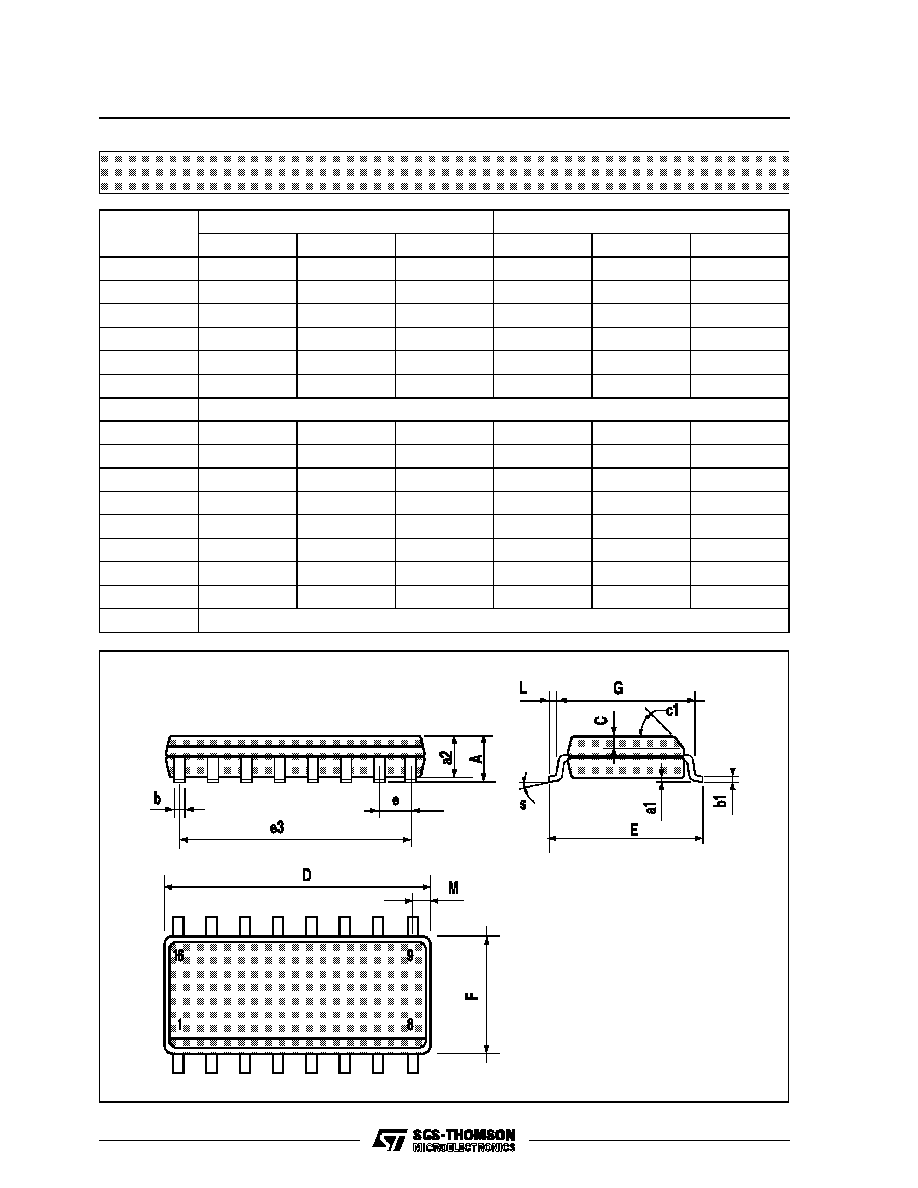
SO16 (Narrow) MECHANICAL DATA
DIM.
mm
inch
MIN.
TYP.
MAX.
MIN.
TYP.
MAX.
A
1.75
0.068
a1
0.1
0.2
0.004
0.007
a2
1.65
0.064
b
0.35
0.46
0.013
0.018
b1
0.19
0.25
0.007
0.010
C
0.5
0.019
c1
45
∞
(typ.)
D
9.8
10
0.385
0.393
E
5.8
6.2
0.228
0.244
e
1.27
0.050
e3
8.89
0.350
F
3.8
4.0
0.149
0.157
G
4.6
5.3
0.181
0.208
L
0.5
1.27
0.019
0.050
M
0.62
0.024
S
8
∞
(max.)
P013H
HCC/HCF4017B/4022B
10/12
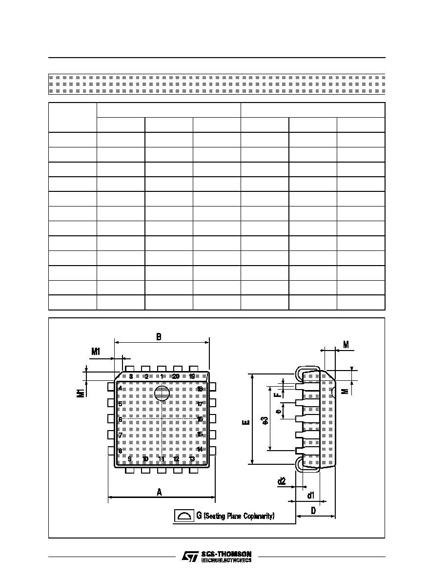
PLCC20 MECHANICAL DATA
DIM.
mm
inch
MIN.
TYP.
MAX.
MIN.
TYP.
MAX.
A
9.78
10.03
0.385
0.395
B
8.89
9.04
0.350
0.356
D
4.2
4.57
0.165
0.180
d1
2.54
0.100
d2
0.56
0.022
E
7.37
8.38
0.290
0.330
e
1.27
0.050
e3
5.08
0.200
F
0.38
0.015
G
0.101
0.004
M
1.27
0.050
M1
1.14
0.045
P027A
HCC/HCF4017B/4022B
11/12
Information furnished is believed to be accurate and reliable. However, SGS-THOMSON Microelectronics assumes no responsability for the
consequences of use of such information nor for any infringement of patents or other rights of third parties which may results from its use. No
license is granted by implication or otherwise under any patent or patent rights of SGS-THOMSON Microelectronics. Specifications mentioned
in this publication are subject to change without notice. This publication supersedes and replaces all information previously supplied.
SGS-THOMSON Microelectronics products are not authorized for use as critical components in life support devices or systems without express
written approval of SGS-THOMSON Microelectonics.
©
1994 SGS-THOMSON Microelectronics - All Rights Reserved
SGS-THOMSON Microelectronics GROUP OF COMPANIES
Australia - Brazil - France - Germany - Hong Kong - Italy - Japan - Korea - Malaysia - Malta - Morocco - The Netherlands -
Singapore - Spain - Sweden - Switzerland - Taiwan - Thailand - United Kingdom - U.S.A
HCC/HCF4017B/4022B
12/12