 | –≠–ª–µ–∫—Ç—Ä–æ–Ω–Ω—ã–π –∫–æ–º–ø–æ–Ω–µ–Ω—Ç: HM6680100 | –°–∫–∞—á–∞—Ç—å:  PDF PDF  ZIP ZIP |
1
ASTEC Semiconductor
AS1431
Precision Adjustable Shunt Reference
Features
•
Temperature-compensated: 30 ppm/°C
•
Trimmed 0.4% bandgap reference
•
Internal amplifier with 150 mA capability
•
Temperature range: Extended to –55
to125°C
•
Low frequency dynamic output
impedance: < 150 mΩ
•
Low output noise
•
Robust ESD protection
Description
The AS1431 is a three-terminal adjustable shunt regulator providing a
highly accurate 0.4% bandgap reference. The adjustable shunt regulator
is ideal for a wide variety of linear applications that can be implemented
using external components to obtain adjustable currents and voltages.
In the standard shunt configuration, the combination of low temperature
coefficient (TC), sharp turn-on characteristics, low output impedance and
programmable output voltage make this precision reference a perfect
zener diode replacement.
The AS1431 is characterized to operate over the full automotive tem-
perature range of –55 to 125°C and is now available in the SOT-23 (5L)
package.
SEMICONDUCTOR
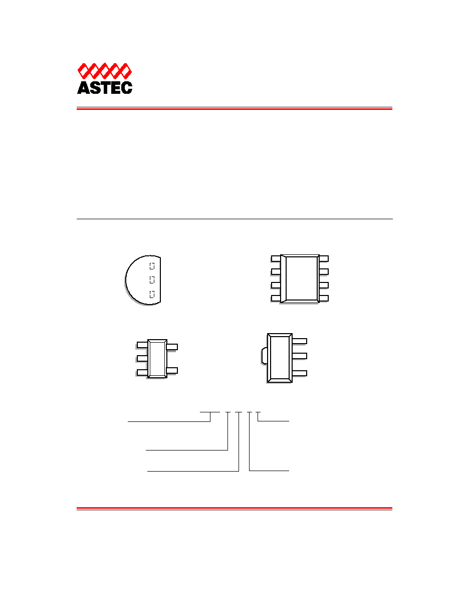
Pin Configuration —
Top view
Ordering Information
CATHODE
TO-92 (LP)
SOIC (D)
ANODE
REFERENCE
CATHODE
REFERENCE
ANODE
ANODE
N/C
CATHODE
ANODE
ANODE
N/C
SOT-89 (S)
SOT-23/5L (DBV)
ANODE
REFERENCE
1
2
3
4
8
7
6
5
REFERENCE
ANODE
N/C
N/C
CATHODE
Circuit Type:
Precision Adjustable
Shunt Regulator
Temperature Range:
D = ≠55
∞
C to +125
∞
C
Bandgap Tolerance:
R4 =
±
0.4%
AS1431 D R4 D 7
Packaging Option:
A
B
T
7
13
Package Style:
D
DBV
LP
S
= SOIC
= SOT-23/5L
= TO-92
= SOT-89
= Ammo Pack
= Bulk
= Tube
= Tape and Reel (7" Reel Dia)
= Tape and Reel (13" Reel Dia)
2
ASTEC Semiconductor
AS1431
Precision Adjustable Shunt Reference
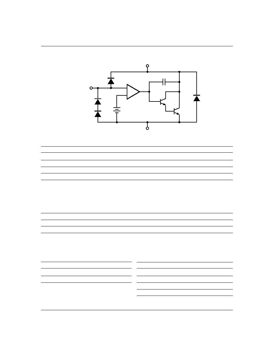
Functional Block Diagram
Absolute Maximum Ratings
Parameter
Symbol
Rating
Units
Cathode-Anode Reverse Breakdown
V
KA
37
V
Anode-Cathode Forward Current
I
AK
1
A
Operating Cathode Current
I
KA
250
mA
Reference Input Current
I
REF
10
mA
Continuous Power Dissipation at 25°C
P
D
TO-92
775
mW
8L SOIC
750
mW
SOT-89
1000
mW
SOT-23/5L
200
mW
Junction Temperature
T
J
150
°C
Storage Temperature
T
STG
–65 to 150
°C
Lead Temperature Soldering 10 Seconds
T
L
300
°C
Stresses greater than those listed under ABSOLUTE MAXIMUM RATINGS may cause permanent damage to the device. This is a
stress rating only and functional operation of the device at these or any other conditions above those indicated in the operational sec-
tions of this specification is not implied. Exposure to absolute maximum rating conditions for extended periods may affect reliability.
–
+
REFERENCE
(R)
ANODE (A)
CATHODE (K)
2.5 V
Recommended Conditions
Parameter
Symbol
Rating
Unit
Cathode Voltage
V
KA
V
REF
to 20
V
Cathode Current
I
K
10
mA
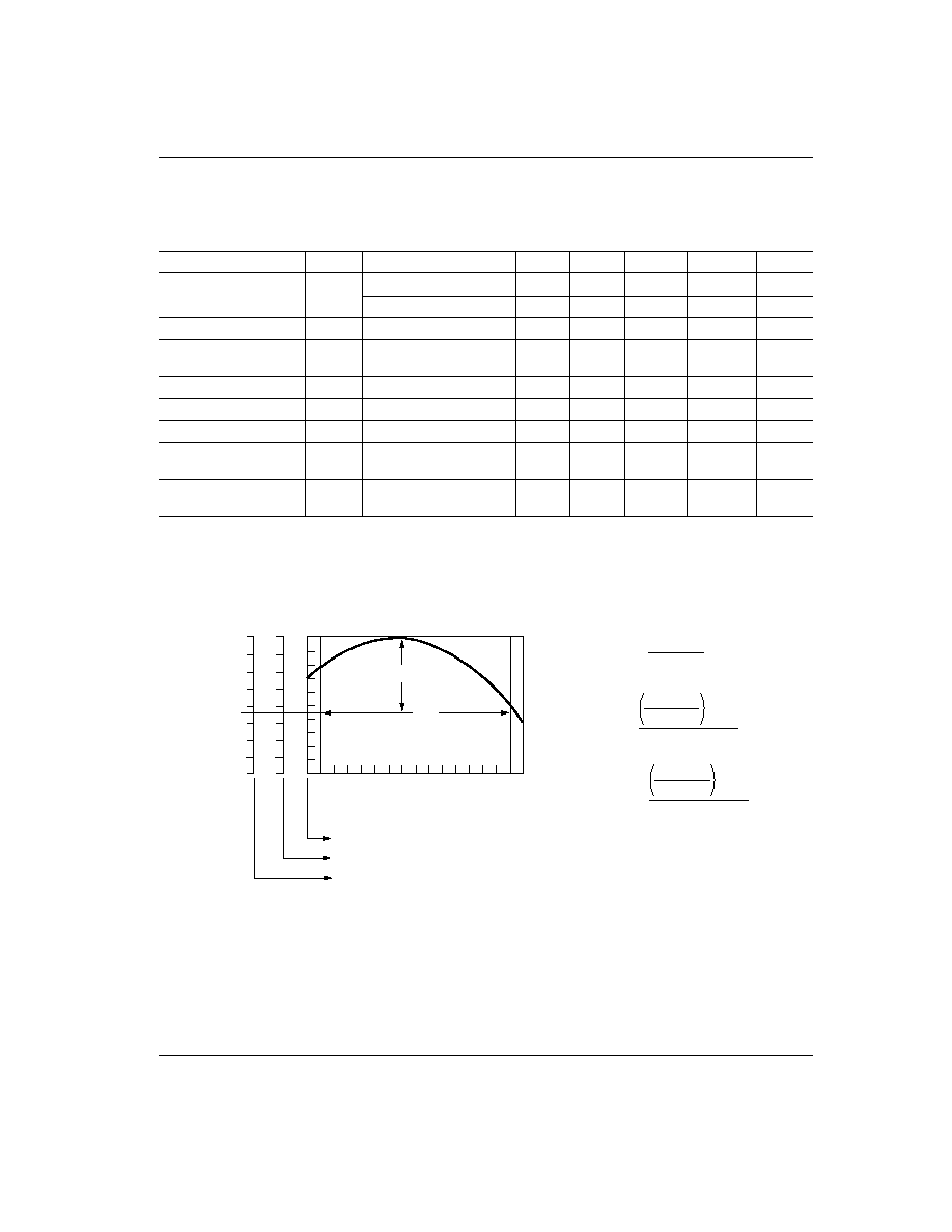
Typical Thermal Resistances
Package
JA
JC
Typical Derating
TO-92
160°C/W
80°C/W
6.3 mW/°C
SOIC
175°C/W
45°C/W
5.7 mW/°C
SOT-89
110°C/W
8°C/W
9.1 mW/°C
SOT-23/5L
575°C/W
150°C/W
1.7 mW/°C
3
ASTEC Semiconductor
AS1431
Precision Adjustable Shunt Reference
Electrical Characteristics
Electrical Characteristics are guaranteed over full junction temperature range (–55 to 125°C). Ambient temperature must be derated
based on power dissipation and package thermal characteristics. The conditions are: V
KA
= V
REF
and I
K
= 10 mA unless otherwise stated.
Parameter
Symbol
Test Condition
Min.
Typ.
Max.
Unit
Circuit
Reference Voltage
V
REF
T
A
= 25°C
2.490
2.500
2.510
V
1
Over temp.
2.470
2.530
V
1
∆V
REF
with Temp*
TC
0.06
0.16
mV/°C
1
Ratio of Change in V
REF
to
∆V
REF
∆V
K
= 3 V to 36 V
–2
–1.1
mV/V
2
Cathode Voltage
Reference Input Current
I
REF
R
1
= 10 k Ω; R
2
= ∞
0.7
1.9
µA
2
I
REF
Temp Deviation
∆I
REF
Over temp.
0.4
1.2
µA
2
Min I
K
for Regulation
I
K(min)
0.4
1
mA
1
Off State Leakage
I
K(off)
V
REF
= 0 V,
0.04
500
nA
3
V
KA
= 36 V
Dynamic Output Impedance
Z
KA
f ≤ 1 kHz
0.15
0.2
Ω
1
I
K
= 1 to 100 mA
*Calculating Average Temperature Coefficient (TC)
0
≠10
≠20
0.5
5000
0
0
≠55 ≠25
0
25
50
75
100
125
0.06 mV/
∞
C
0.002%/
∞
C
24 ppm/
∞
C
ppm
mV
%
V
REF
T
Temperature (
∞
C)
∑ TC in mV/
∞
C =
∑ TC in %/
∞
C =
T
A
T
A
X 100
V
REF
(mV)
V
REF
at 25
∞
C
V
REF
∑ TC in ppm/
∞
C =
T
A
X 10
6
V
REF
at 25
∞
C
V
REF
Average Temperature Coefficient
4
ASTEC Semiconductor
AS1431
Precision Adjustable Shunt Reference
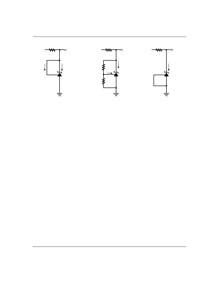
Test Circuits
Figure 1a. Test Circuit 1
Figure 1b. Test Circuit 2
Figure 1c. Test Circuit 3
R
1
R
2
I
K
V
IN
V
KA
(V
REF
)
I
REF
I
REF
I
K
V
IN
V
KA
=
V
REF
I
K (OFF)
V
IN
V
KA
5
ASTEC Semiconductor
AS1431
Precision Adjustable Shunt Reference
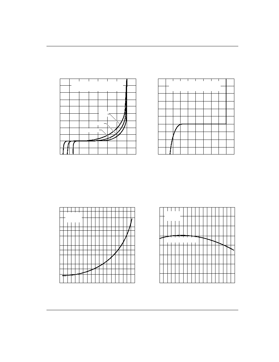
Typical Performance Curves
Figure 2
Figure 4
Figure 3
Figure 5
I
K
≠ Cathode Current (
µ
A)
900
700
600
500
400
300
200
100
0
≠100
≠200
800
≠1.0
0
1.0
V
KA
≠ Cathode Voltage (V)
2.0
3.0
Low Current Operating Characteristics
V
KA
= V
REF
Temperature Range: ≠55 to 125
∞
C
125
∞
C
25
∞
C
≠55
∞
C
I
K
≠ Cathode Current (mA)
150
125
100
75
50
25
0
≠25
≠50
≠75
≠100
≠2
≠1
0
1
2
3
V
KA
≠ Cathode Voltage (V)
High Current Operating Characteristics
V
KA
= V
REF
Temperature Range: ≠55 to 125
∞
C
I
Z
off ≠ Off State Cathode Current (nA)
100
10
1
0.1
0.01
≠60
≠30
0
30
T
A
≠ Ambient Temperature (
∞
C)
60
90
120
Off State Leakage
V
KA
= 36 V
V
REF
= 0 V
V
REF
≠ Reference V
oltage (V)
2.53
2.52
2.51
2.50
2.49
2.48
2.47
2.46
2.45
≠60
≠30
0
30
T
A
≠ Ambient Temperature (
∞
C)
60
90
120
V
KA
= V
REF
I
K
= 10 mA
Reference Voltage vs Ambient Temperature
V
REF
= 2.500 V at 25
∞
C