 | ÐлекÑÑоннÑй компоненÑ: HP7501 | СкаÑаÑÑ:  PDF PDF  ZIP ZIP |
Äîêóìåíòàöèÿ è îïèñàíèÿ www.docs.chipfind.ru
HP7501
Ultra320 LVD/SE SCSI Terminator
2003/05/12 Ver. 0.0
1
HIMARK TECHNOLOGY INC.
FEATURES
Fully compliant with Ultra320 (SPI-4),
Ultra3/Ultra160 (SPI-3), Ultra2/Fast-40 (SPI-2)
and Ultra/Fast-20 Standards.
Auto Selection Multi-Mode SE or LVD
Termination for 9 signal line pairs.
Built-in SPI-4 Mode Change Filter
2.7V to 5.25V Operation
Built in Current Limit and Thermal shutdown
Protection Circuitry.
Support Master/Slave input.
SCSI bus hot plug compatible.
Support active negation drive.
28 and 36 pin package.
DESCRIPTION
The HP7501 is a multi-mode SCSI terminator that
conforms to the SCSI (SPI-4) specification which is
designed for the low voltage differential (LVD)
termination. The HP7501 provides backward
c om patibility to the SCSI-2, SCSI-1 and a
Single-Ended specifications.
Multi-mode function set up the use of legacy devices
on the bus without changing any hardware setting.
Automatic selection is made by voltage detection on
the DIFFSEN line. If the device is connected in an
LVD only bus, the HP7501 will use LVD termination. If
the device is connected in a Single Ended mode, the
H P 7 5 0 1 wi l l c o n n ec t i n a S E t e rm i n a ti o n.
HiMARK's SCSI termination architecture uses high
speed elements for the design, therefore providing the
fast response time.
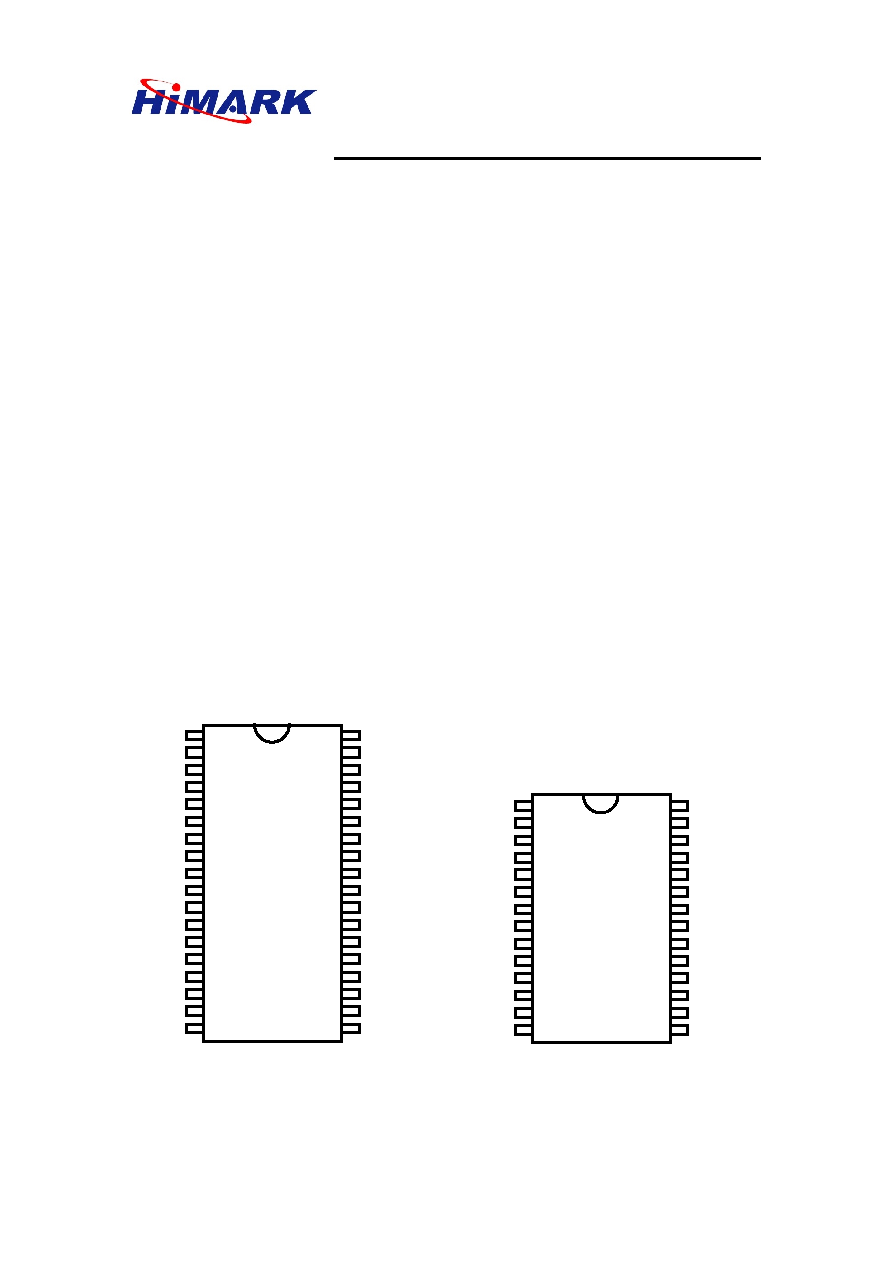
PACKAGE PINOUT
VREF
NC
R1P
NC
R1N
R2P
HGND
R2N
HGND
HGND
R3N
R3P
R4P
R4N
R5N
R5P
ISO
GND
1
2
4
3
5
6
8
7
9
10
12
11
36
35
33
34
32
31
29
30
28
27
25
26
13
14
16
15
17
18
24
23
21
22
20
19
HP7501-A36
TPWR
HVD
SE
LVD
R9N
R9P
R8P
R8N
HGND
HGND
R7N
HGND
R7P
R6N
DIF_CAP
R6P
DIFFSENSE
MST/SLV
VREF
R1P
R2P
R1N
R2N
HGND
R3N
R3P
R4P
R4N
R5N
R5P
ISO
GND
1
2
4
3
5
6
8
7
9
10
12
11
28
27
25
26
24
23
21
22
20
19
17
18
13
14
16
15
HP7501-T28
TPWR
TPWR
R9P
R9N
R8N
R8P
R7N
HGND
R7P
R6N
DIF_CAP
R6P
DIFFSENSE
MST/SLV
HP7501
Ultra320 LVD/SE SCSI Terminator
2003/05/12 Ver. 0.0
2
HIMARK TECHNOLOGY INC.
ORDERING INFOMATION
PART NUMBER
PIN - PACKAGE
HP7501-A36 SSOP-36
pin
HP7501-T28 TSSOP-28
pin
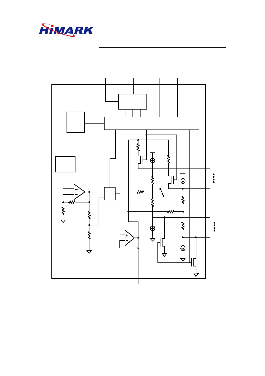
FUNCTIONAL DESCRIPTION
HP 7501 is a multi-mode active terminator with
automatically switching on LVD/SE/HVD mode. The
DIFFSENS* is on one of three voltage levels to indicate
LVD/SE/HVD mode. If the voltage on DIFFSESE** is
above 2.16V, below 0.6V or between, that indicates the
bus mode to be HVD, SE, or LVD.
In Figure 1, a bandgap reference is fed into an buffer
to generate reference voltages. A voltage selected by the
control logic through a MUX is used to generate 2.85V or
1.25V reference voltages. A voltage 2.85V and 1.25V is
used in SE mode and LVD mode respectively. The
voltage for a specific mode is sent out through an op
buffer. In SE mode, the RxP pin is switched to ground.
DIFF_CAP with a RC low pass filter monitors the
voltage on DIFFSENS to determine the termination mode
used on bus. The DIFFERENSE CIRCUITRY decodes
the trinary voltage on DIFF_CAP and generates three
control logic signals internally. The control logic will
change the total termination resistance and switch to one
of three termination modes based on the voltage on
DIFFSENS.
SE Mode
: The voltage on DIFFSENSE is between
0V - 0.5V. RxP pin is grounded. When the external driver
for a given line turns off, the active terminator will pull
that signal line to 2.85V (quiescent state). When
operated in an active negation driver, the power amp can
sink 22mA per line and the reference voltage won't
change over 100mV. The termination resistors maintain
110ohm.
HVD Mode
: The voltage on DIFFSENSE is above
2.4V. HP7501 will identify that there is an HVD (high
voltage differential) device on the SCSI bus and isolate
the termination pins from the bus.
LVD Mode
: The voltage on DIFFSENSE is between
0.71.9V. A precious resistor string between two current
sources provides LVD termination. It offers a 105 ohm
differential mode impedance and a 125 ohm common
mode impedance. A fail-safe bias of 112mV is maintained
when no driver is connected to the SCSI bus.
During high temperature (>150 ), HP7501 would
thermal shutdown. The termination pins are isolated from
SCSI bus and Vref becomes high impedance. When
ISO=1, the termination pins are isolated from the SCSI
bus, but the bus mode indicators (SE/LVD/HVD) and Vref
remain active. In the above two cases, the DIFFSENSE
driver is shut down and in high impedance.
The TPWR pin is connected to the SCSI bus
TERMPWR line to power up the HP7501. The TERMPWR
line should be bypassed locally. A 2.2uF capacitor and a
0.01uF high frequency capacitor between TPWR and
ground are suggested for different frequency noise.
Capacitors should be placed as close as possible to the
HP7501. The HP7501 should be placed as close as
possible to the SCSI connector to minimize input signal
trace length and result in less reflections and better
performance.
To maintain the specified voltage, a 4.7uF capacitor is
recommended between the Vref (pin36) and ground. A
high frequency capacitor (0.1uF ceramic recommended)
can also be placed on the Vref pin in applications the use
fast rise/fall time drivers. It is also recommended to place
a RC low pass filter between DIFFSENSE and DIF_CAP
to lower noise from the SCSI bus.
DIFFSENS Noise Filtering
: The HP7501
incorporates a digital filter to remove high frequency
transients on the DIFFSENS control line. The external
filter may be used as well in addition to the internal digital
filter.
A typical SCSI bus configuration is shown in Figure 2.
NOTE:
* DIFFSENS: Refers to the SCSI bus signal
** DIFFSENSE: Refers to the pin name in HP7501.
HP7501
Ultra320 LVD/SE SCSI Terminator
2003/05/12 Ver. 0.0
3
HIMARK TECHNOLOGY INC.
BLOCK DIAGRAM
CONTROL
LOGIG
DIFFSENSE
CIRCUITRY
THERMAL
SHUTDOWN
CIRCUITRY
BANDGAP
REFERENCE
1.25V
DIF_CAP
DIFFSENSE
MUX
ISO
MSTR/SLV
2.85V
R1P
124 Ohm
R1N
52 Ohm
52 Ohm
VREF
SE
GND
DRIVER
R1se
R9P
124 Ohm
R9N
52 Ohm
52 Ohm
SE
GND
DRIVER
R2se
Figure 1. Block Diagram of HP7501
HP7501
Ultra320 LVD/SE SCSI Terminator
2003/05/12 Ver. 0.0
4
HIMARK TECHNOLOGY INC.
PIN DESCRIPTION ( for 36pin SSOP)
PIN SYMBOL
DESCRIPTION
36 TPWR
2.7V to 5.25V power input pin. Connect to SCSI bus power line. A 4.7µF
capacitor and a 0.1µF high frequency capacitor are recommended between
TPWR and ground
1 VREF
Reference Voltage. Must be decoupled with a 4.7uF as shown in Figure 1.
2,3
NC
Do not connect any signal to this pin.
8,9,10
26,27,28
HGND
Heat Sink Ground. Connect to large area PC board ground trace in order to
increase power dissipation.
4,6,11,13,15
22,24,29,31
RxP
Termination lines. These lines switch to hard ground in SE mode and are the
positive lines for LVD mode. All lines are in high impedance when HVD is
detected.
5,7,12,14,16
23,25,30,32
RxN
Termination lines. These lines switch to the active lines in SE mode and are the
negative lines for LVD mode. All lines are in high impedance when HVD is
detected.
17 ISO
Isolation pin. This pin is used to shut down the terminator if the terminator is
not connected at the end of the bus. Connect the pin to ground will activate the
terminator in normal operation. The terminator will be disabled when the pin is
in high state. An internal pull-down resistor assures that the HP7501 will
operate as normal if the ISO pin is left floating.
18 GND
Signal
Ground.
19 MST/SLV
Mode select pin. When pull high, master mode will enable the DIFFSEN drive
SCSI bus. The DIFFSENSE driver is off when this pin is connected to ground.
20 DIFFSENSE
This signal will drive 1.3V to the SCSI bus during the Master mode in order to
detect which type of device is connected to the SCSI bus. On power up, the
HP7501 will try to deliver LVD level to the DIFFSENSE line. If only LVD SCSI
devices are on the bus, the DIFFSENSE signal will be successfully driven to
1.3V and the terminator will configure the system for LVD operation. If any SE
device is on the bus, it will present a grounding level to the DIFFSENSE line.
This will indicate HP7501 to configure into SE operation. HP7501 will be in shut
down mode if DIFFSENSE detects a high voltage level.
21 DIF_CAP
This pin should be connected to a 0.1uF capacitor to ground and 20K resistor
to SCSI bus DIFFSENS line for DIFFSEN filter.
33
SE
Single ended. Indicates SE device is on the SCSI bus when this pin is active.
34
LVD
Low Voltage Differential. Indicates the terminator is in LVD operation.
35 HVD
High Voltage Differential. Indicates the HVD device is detected and terminator
is in shut down mode.
PIN DESCRIPTION ( for 28pin TSSOP)
PIN
SYMBOL
DESCRIPTION
27,28 TPWR
2.7V to 5.25V power input pin. Connect to SCSI bus power line. A 4.7µF
capacitor and a 0.1µF high frequency capacitor are recommended between
TPWR and ground.
1 VREF
Reference Voltage. Must be decoupled with a 4.7uF as shown in Figure 1.
6,22 HGND
Heat Sink Ground. Connect to large area PC board ground trace in order to
increase power dissipation.
2,4,7,9,11
18,20,23,25
RxP
Termination lines. These lines switch to hard ground in SE mode and are the
positive lines for LVD mode. All lines are in high impedance when HVD is
detected.
3,5,8,10,12
19,21,24,26
RxN
Termination lines. These lines switch to the active lines in SE mode and are the
negative lines for LVD mode. All lines are in high impedance when HVD is
detected.
13 ISO
Isolation pin. This pin is used to shut down the terminator if the terminator is
not connected at the end of the bus. Connect the pin to ground will activate the
terminator in normal operation. The terminator will be disabled when the pin is
in high state. An internal pull-down resistor assures that the HP7501 will
operate as normal if the ISO pin is left floating.
HP7501
Ultra320 LVD/SE SCSI Terminator
2003/05/12 Ver. 0.0
5
HIMARK TECHNOLOGY INC.
14 GND
Signal
Ground.
15 MST/SLV
Mode select pin. When pull high, master mode will enable the DIFFSEN drive
SCSI bus. The DIFFSENSE driver is off when this pin is connected to ground.
16 DIFFSENSE
This signal will drive 1.3V to the SCSI bus during the Master mode in order to
detect which type of device is connected to the SCSI bus. On power up, the
HP7501 will try to deliver LVD level to the DIFFSENSE line. If only LVD SCSI
devices are on the bus, the DIFFSENSE signal will be successfully driven to
1.3V and the terminator will configure the system for LVD operation. If any SE
device is on the bus, it will present a grounding level to the DIFFSENSE line.
This will indicate HP7501 to configure into SE operation. HP7501 will be in shut
down mode if DIFFSENSE detects a high voltage level.
17 DIF_CAP
This pin should be connected to a 0.1uF capacitor to ground and 20K resistor
to SCSI bus DIFFSENS line for DIFFSEN filter.
RECOMMENDED OPERATING CONDITIONS
PARAMETER SYMBOL
MIN
TYP
MAX
UNITS
NOTES
Termpower Voltage (SE)
Termpower Voltage (LVD)
Vtpwr
4.0
2.7
5.25
5.25
V
V
Logic 0 (Low)
Logic 1 (High)
V
il
V
ih
-0.3
2.0
+0.8
Vtpwr+0.3
V
V
Operating Temperature
Ta
0
70
DC CHARACTERISTICS
PARAMETER SYMBOL
MIN TYP MAX
UNITS
NOTES
TPWR Current (SE)
TPWR Current (LVD)
Itpwr
Itpwr
15
25
mA
mA
*1
Input Leakage Current
High
Iih 0
uA
Input Leakage Current
Low
Iil 1.0
uA
Output Current High
Vout = 2.4 V
Ioh 0
mA
Output Current Low
Vout = 0.4V
Iol 4.0
mA
DIFFSEN Output Voltage
Vov
1.2
1.4
V
DIFFSEN Source Current
Isc
5
15
mA
DIFFSEN Sink Current
Isi
20
200
uA
DIFFSEN SE
Voltage Range
Vse -0.3 0.5 V
DIFFSEN LVD
Voltage Range
Vlvd 0.7 1.9 V
DIFFSEN HVD
Voltage Range
Vhvd 2.4
Vtpwr+0.3
V
HP7501
Ultra320 LVD/SE SCSI Terminator
2003/05/12 Ver. 0.0
6
HIMARK TECHNOLOGY INC.
SINGLE ENDED CHARACTERISTICS
PARAMETER SYMBOL
MIN TYP MAX
UNITS
NOTES
SE Termination Resistance
Rse
104.5
110
115.5
SE Voltage Reference
Vref
2.70
3.00
V
SE Output Current
Ioc
25.4
mA
*2
LVD CHARACTERISTICS
PARAMETER SYMBOL
MIN TYP MAX
UNITS
NOTES
Differential Mode Termination
Resistance
Rdm 100 110
Common Mode Termination
Resistance
Rcm 110 125 150
Differential Mode Bias
All lines open
Vdb 100 112 125
mV
Common Mode Bias
Vcb
1.125
1.250
1.375
V
REGULATOR CHARACTERISTICS
PARAMETER SYMBOL
MIN
TYP
MAX
UNITS
NOTES
Source Current
Isour
200
230
mA
*3
Sink Current
Isink
100
200
mA
NOTE: Unless otherwise specified, these specifications apply over the operating ambient temperature range from 0
to 70.
*1. All lines open.
*2. Vline = 0.2V
*3. Vref = 0.2V
HP7501
Ultra320 LVD/SE SCSI Terminator
2003/05/12 Ver. 0.0
7
HIMARK TECHNOLOGY INC.
TYPICAL OPERATING CIRCUIT
TPWR
MST/SLV
ISO
TPWR
MST/SLV
ISO
TPWR
MST/SLV
ISO
TPWR
MST/SLV
ISO
TPWR
MSTSLV
ISO
TPWR
MST/SLV
ISO
VREF
DIF_CAP
VREF
DIF_CAP
DIF_CAP
VREF
DIFFSENSE
DIFFSENSE
20k
20k
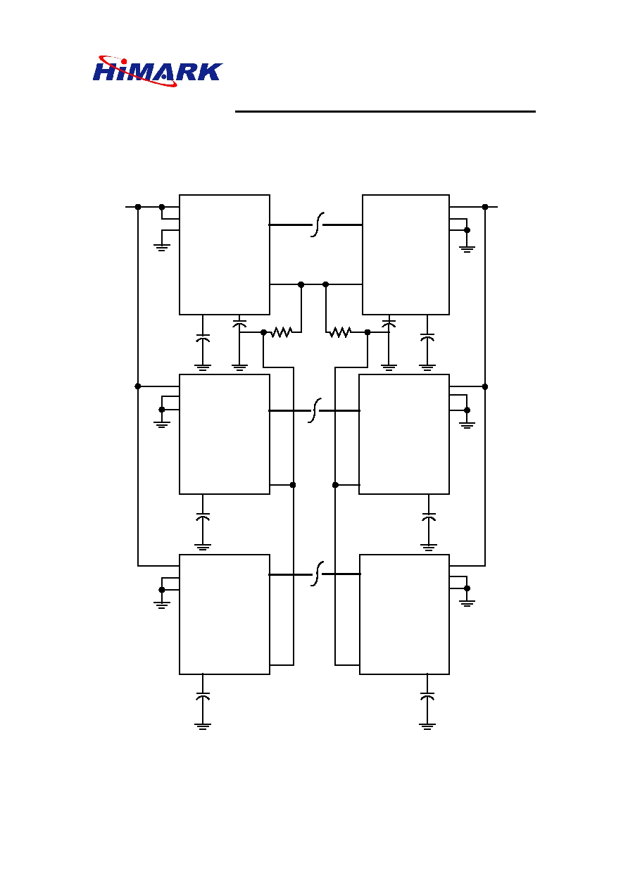
Figure 2. SCSI BUS Configuration
0.1uF
4.7uF
0.1uF
TERMPWR
4.7uF
4.7uF
4.7uF
TERMPWR
DATA
DATA
CONTROL
HP7501
HP7501
HP7501
HP7501
HP7501
HP7501
VREF
VREF
VREF
DIF_CAP
DIF_CAP
DIF_CAP
4.7uF
4.7uF
HP7501
Ultra320 LVD/SE SCSI Terminator
2003/05/12 Ver. 0.0
8
HIMARK TECHNOLOGY INC.
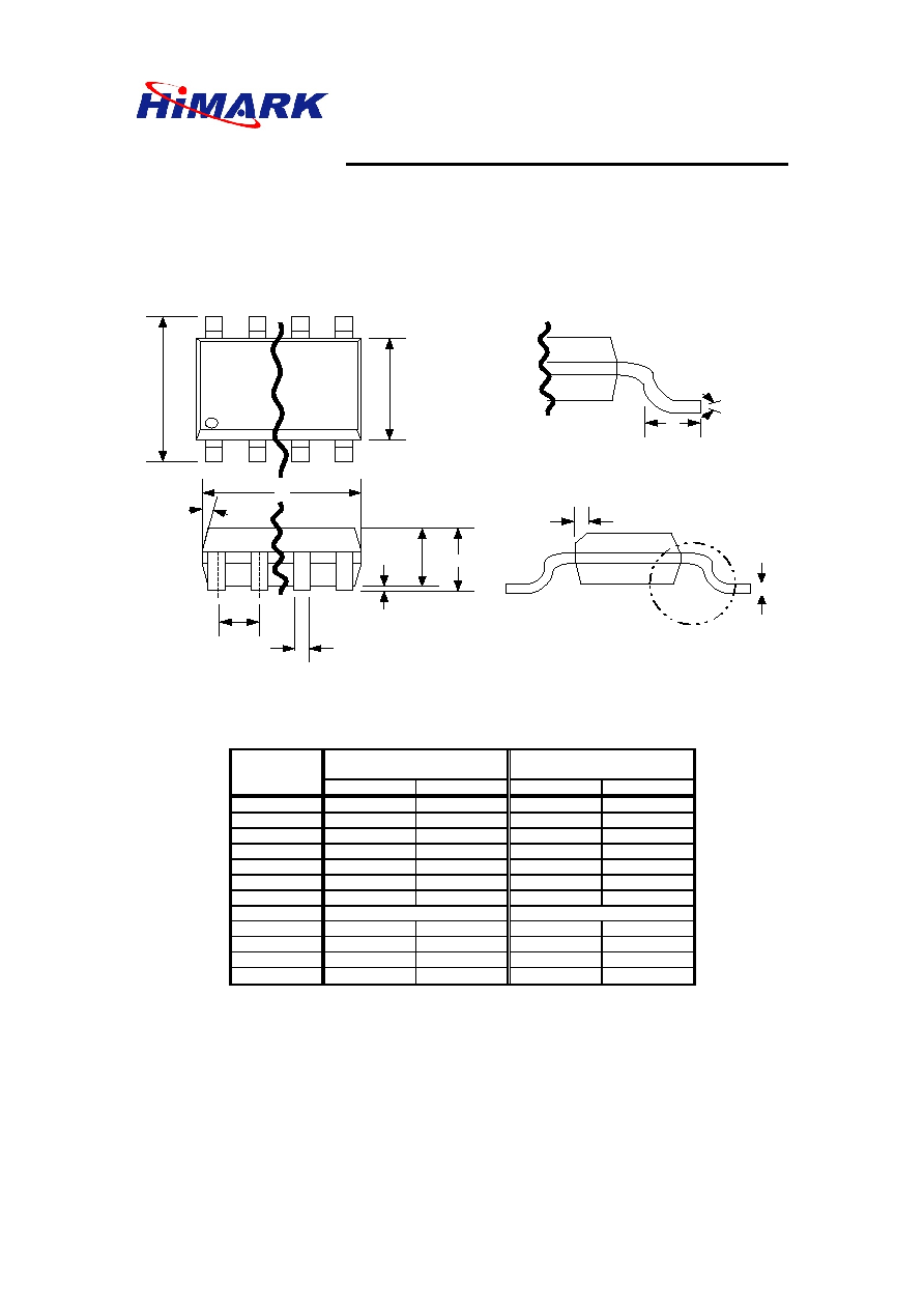
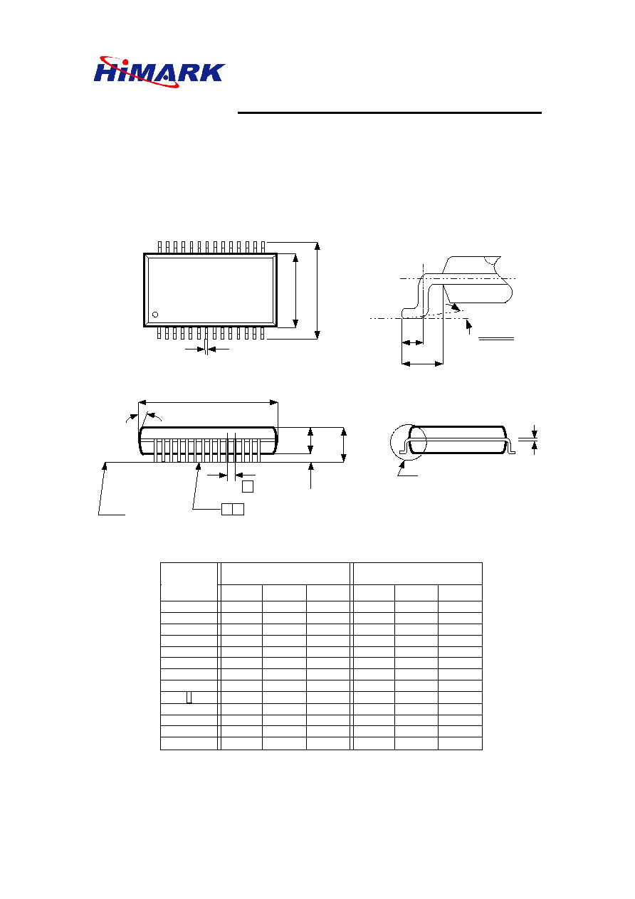
PACKAGE DIMENSION
The package of HP7501-A36 is SSOP-36
D
T (4X)
A
B
e
0.015x45
0
C
L
Q
H
E
V iew A
A1
A2
SSOP-36
DIMENSIONS IN
MILLIMETERS
DIMENSIONS IN
INCHES
SYMBOL
MIN MAX MIN MAX
A
2.41 2.59 0.095 0.110
A1
0.20 0.40 0.008 0.016
A2
2.26 2.52 0.089 0.099
B
0.30 0.45 0.012 0.018
C
0.127 0.254 0.005 0.010
D
15.75 16.00 0.620 0.630
E
7.391 7.595 0.291 0.299
e
0.8BSC 0.032BSC
H
10.033 10.668 0.395 0.420
L
0.508 1.016 0.020 0.040
T
---- 0.10 ---- 0.004
0
°
8
°
0
°
8
°
HP7501
Ultra320 LVD/SE SCSI Terminator
2003/05/12 Ver. 0.0
9
HIMARK TECHNOLOGY INC.
The package of HP7501-T28 is TSSOP-28
1
4
1
15
28
E
H
b
D
e
Seating Plane
A
1
A
2
A
L
See Detail F
C
Detail F
12°(4X
)
L
1
D y
DIMENSIONS IN
MILIMETERS
DIMENSIONS IN
INCHES
SYMBOLS
MIN
NOM
MAX
MIN
NOM
MAX
A
1.20
0.047
A1
0.05
0.15
0.002
0.006
A2
0.80
1.00
1.05
0.031
0.039
0.041
b
0.19
0.3 0
0.007
0.012
C
0.09
0.20
0.004
0.008
D
9.60
9.70
9.80
0.378
0.382
0.385
H
6.40
0.252
E
4.30
4.40
4.50
0.169
0.173
0.177
e
0.65
0. 026
L
0.45
0.60
0.75
0.018
0.024
0.030
L1
1.00
0.039
y
0.076
_____
0.003
0°
8°
0°
8°
TSSOP-28
_____
_____
_____
_____
_____
_____
_____
_____
_____
_____
_____
_____
_____
_____
_____
_____
_____
_____
_____
_____
_____
_____
_____
_____
_____
_____
_____
HMARK reserves the right to make changes without further notice herein.