Description
The i72120 GPIB-Chip is the ideal solution to implement a
IEEE488.2 GPIB interface for next generation PCI based
instruments. The GPIB-ASIC is designed to meet all of the
functional requirements for talker and listener (TL) devices
as specified by the IEEE Standards 488.1-1987 and
488.2-1987. Connected between the PCI bus and the GPIB,
this GPIB-IC provides high-level management of the GPIB to
unburden the processor and to simplify both hardware and
software design. The i72120 is fully compatible with the PCI
specification and requires only the addition of bus
driver/receiver components to implement a talker/listener
GPIB interface.
History
The IEEE Standard 488 describes a "Standard Digital Interface
for Programmable Instrumentation" which, since its
introduction in 1975 has become the most popular means of
interconnecting instruments and controllers in laboratory,
automatic test, and even industrial applications. Refined over
several years, the 488-1978 Standard, also known as The
General Purpose Interface Bus (GPIB), is a highly
sophisticated standard providing a high degree of of flexibility
to meet virtually all instrumentation requirements. The
i72120 implements all of the functions that are required to
interface to the GPIB as a talker or listener device. While it
is beyond of the scope of this document to provide a complete
explanation of the IEEE 488 Standard, a basic descriprion
follows:
The GPIB interconnects up to 15 devices over a commom
set of data control liners. Three types of devices are defined
by the standard: talker, listener, and controller, atthough
some devices may combine functions such as talker/listener
or talker/controller.
Data on the GPIB is transferred in a bit-parallel,
byte-serial fashion over eight data I/O lines
(/DIO[1]-/DIO[8]). A three-wire handshake is used to ensure
synchronisation of transmission and reception. In order to
permit more than one device to receive data at the same time,
these control lines are "open collector" so that the slowest
device controls the data rate. A number of other control lines
perform a variety of functions such as device addressing,
interrupt generation and so forth.
The i72120 implements all functional aspects of talker
and listener as defined by the 488.1-1987 Standard on a
single chip.
Pin Functions
Pinout
Type
Function
Pin
Type
Function
Pin
OUTPUT
NRFDoen
2
OUTPUT
NDACoen
1
INPUT
PCI_RSTNi
4
OUTPUT
RENo
3
OUTPUT
SRQoen
6
NC
NC
5
INPUT
ATNi
8
VCC
VCC
7
INPUT
EOIi
10
INPUT
DAVi
9
INPUT
SRQi
12
INPUT
IFCi
11
INPUT
NRFDi
14
INPUT
RENi
13
INPUT
NDACi
16
GND
GND
15
PDN
PDN
18
PDN
PDN
17
INPUT
RSTN
20
VCC
VCC
19
VCC
VCC
22
INPUT
CLK
21
BIDIR
AD[31]
24
OUTPUT
INTAon
23
BIDIR
AD[29]
26
BIDIR
AD[30]
25
BIDIR
AD[27]
28
BIDIR
AD[28]
27
GND
CND
30
BIDIR
AD[26]
29
ine s
ine s
Advance Information
Datasheet i72120
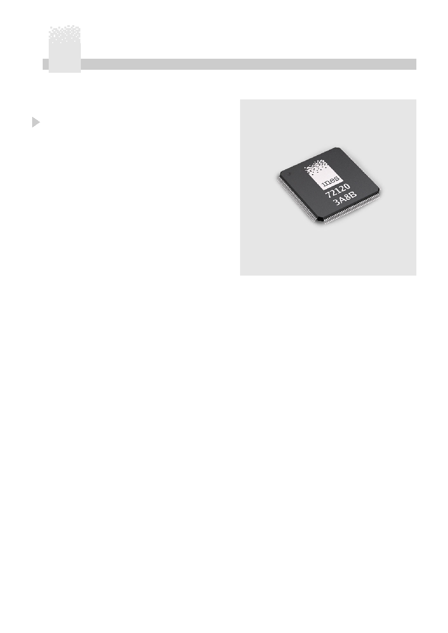
i72120
PCI to GPIB interface ASIC
Features
∑
Talker/Listener interface for instrumentation
devices
∑
PCI v2.2 32-bit/33MHz Target with 3.3 VCC,
3.3/5.0 VIO
∑
NEC µPD7210 compatible register layout
∑
144 pin TQFP package
∑
RoHS conformant (Pb-free)
XSL
∑
FO
RenderX

Type
Function
Pin
Type
Function
Pin
BIDIR
AD[24]
32
BIDIR
AD[25]
31
INPUT
IDSEL
34
INPUT
CBEN[3]
33
BIDIR
AD[22]
36
BIDIR
AD[23]
35
PUP
PUP
38
BIDIR
AD[21]
37
BIDIR
AD[19]
40
BIDIR
AD[20]
39
VCC
VCC
42
BIDIR
AD[18]
41
BIDIR
AD[16]
44
BIDIR
AD[17]
43
INPUT
FRAMEN
46
INPUT
CBEN[2]
45
BIDIR
TRDYN
48
INPUT
IRDYN
47
GND
GND
50
BIDIR
DEVSELN
49
BIDIR
PERRN
52
BIDIR
STOPN
51
GND
GND
54
BIDIR
SERRN
53
INPUT
CBEN[1]
56
BIDIR
PAR
55
VCCIO
VCCIO
58
BIDIR
AD[15]
57
BIDIR
AD[13]
60
BIDIR
AD[14]
59
BIDIR
AD[11]
62
BIDIR
AD[12]
61
BIDIR
AD[9]
64
BIDIR
AD[10]
63
GND
GND
66
BIDIR
AD[8]
65
BIDIR
AD[7]
68
INPUT
CBEN[0]
67
BIDIR
AD[5]
70
BIDIR
AD[6]
69
INPUT
HIGH
72
INPUT
LOW
71
BIDIR
AD[3]
74
BIDIR
AD[4]
73
BIDIR
AD[1]
76
BIDIR
AD[2]
75
INPUT
PDN
78
BIDIR
AD[0]
77
BIDIR
NC
80
VCC
79
BIDIR
NC
82
INPUT
PDN
81
BIDIR
NC
84
BIDIR
NC
83
BIDIR
NC
86
BIDIR
NC
85
BIDIR
NC
88
GND
GND
87
CLKPAD
PDN
90
CLKPAD
PDN
89
CLKPAD
PDN
92
VCC
VCC
91
VCC
VCC
94
CLKPAD
PDN
93
OUTPUT
NC
96
BIDIR
NC
95
OUTPUT
NC
98
OUTPUT
NC
97
INPUT
PDN
100
OUTPUT
NC
99
GND
GND
102
INPUT
PDN
101
INPUT
DIOi[1]
104
OUTPUT
NC
103
INPUT
DIOi[3]
106
INPUT
DIOi[2]
105
INPUT
DIOi[5]
108
INPUT
DIOi[4]
107
INPUT
LOW110
110
INPUT
LOW109
109
INPUT
DIOi[7]
112
INPUT
DIOi[6]
111
VCC
VCC
114
INPUT
DIOi[8]
113
OUTPUT
DIOoen[1]
116
OUTPUT
DIOo[1]
115
OUTPUT
DIOoen[2]
118
OUTPUT
DIOo[2]
117
OUTPUT
DIOoen[3]
120
OUTPUT
DIOo[3]
119
GND
GND
122
OUTPUT
DIOo[4]
121
OUTPUT
DIOo[5]
124
OUTPUT
DIOoen[4]
123
GND
126
OUTPUT
DIOoen[5]
125
OUTPUT
DIOoen[6]
128
OUTPUT
DIOo[6]
127
VCCIO
VCCIO
130
OUTPUT
DIOo[7]
129
OUTPUT
DIOo[8]
132
OUTPUT
DIOoen[7]
131
OUTPUT
ATNo
134
OUTPUT
DIOoen[8]
133
OUTPUT
DAVo
136
OUTPUT
ATNoen
135
GND
GND
138
OUTPUT
DAVoen
137
OUTPUT
EOIoen
140
OUTPUT
EOIo
139
OUTPUT
IFC_RENoen
142
OUTPUT
IFCo
141
INPUT
LOW144
144
NC
143
Specifications
GPIB Capabilities
IEEE 488.1 Capabilities: AH1, SH1, T/TE5, L/LE3, SR1,
RL1, PP1/PP2, DC1, DT1, C0
GPIB Handshake Rate: > 1Mbytes/sec
Environmental and Physical
Package: 144 TQFP, 22.0 mm x 22.0 mm x 1.6 mm
Storage Temperature: -20...80∞C
Ambient Temperature: -0...70∞C
ine s
ine s
Advance Information
Datasheet i72120 (cont.)
XSL
∑
FO
RenderX

Ordering Information
i72120-33
- Tray of 60 units
On the Web
Click
www.inesinc.com
for more information and resources.
This document contains information on products under development by INES.
The information is intended to help you evaluate this product. INES reserves
ines Test and Measurement GmbH & Co. KG
ine s
the right to change oder discontinue work on this proposes product without
notice. All specifications are subject to change without notice. Copyright ©
2005. All rights reserved.
31542 Bad Nenndorf ∑ DE (Germany)
Phone +49 5723 916 250
Fax +49 5723 916 252
Web
www.inesinc.com
ine s
ine s
Advance Information
Datasheet i72120 (cont.)
XSL
∑
FO
RenderX