 | –≠–ª–µ–∫—Ç—Ä–æ–Ω–Ω—ã–π –∫–æ–º–ø–æ–Ω–µ–Ω—Ç: I80234 | –°–∫–∞—á–∞—Ç—å:  PDF PDF  ZIP ZIP |

THE ADSL TECHNOLOGY COMPANY
©
Integrated Telecom Express, Inc. Preliminary Specification, Confidential and Proprietary, Subject to Change Without Notice
i80234 - Analog Front End
Chipset Solutions
Integrated Telecom Express
is a leading innovator and manufacturer of
Asymmetric Digital Subscriber Line (ADSL) OEM chips.
Interoperable
ITeX products adhere to all ANSI and ITU specifications.
ITeX's participation in all the major standards groups, including DSL Forum,
ISWG and UNH-IOL offer assured interoperability worldwide.
Compatible
With the ITeX i90135 and i90816.
Introduction
The ITeX Analog Front End (i80234) analog IC is a highly integrated analog front end and an optimized
solution for ANSI T1.413, G.992.1, and G.992.2 ATU-R modems. It is based on the i80134 specifications
with an addition of a low noise receiver. It is the basis of a highly integrated AFE circuit, requiring only the
addition of a line driver. Therefore, it provides a very cost-effective solution for ADSL Customer Premise
Equipment (CPE).
Features
!
!
!
!
Built-in low noise programmable amplifier
with a gain range from 0 to 49 dB
!
!
!
!
8.8 MHz per second ADC, 13 bits
!
!
!
!
8.8 MHz per second DAC, 12 bits
!
!
!
!
8-bit DAC for timing recovery
!
!
!
!
Built-in variable capacitor for timing
recovery
!
!
!
!
4 bit digital interface for data transfer
!
!
!
!
1V full scale input
!
!
!
!
Differential analog I/O
!
!
!
!
64 pin LQFP package
!
!
!
!
0.53 watts at 3.3V
!
!
!
!
3rd and 4th order tunable continuous time
low pass filters for channel filtering
!
!
!
!
Selectable low pass filter in the transmission
path for both G.992.1 Annex A and B
support
Benefits
!
!
!
!
The i80234 has programmable low pass
filters and automatic gain control in both the
transmission and receiving directions. The
filters feature a programmable cutoff
frequency and use automatic continuous
time tuning to avoid a time varying phase
characteristic optimized for, DMT, ATU-R
operation. Programmable for ITU-T G.992.1
Annex A and B support.
!
!
!
!
Built-in 9-bit DAC and variable capacitors,
the i80234 can use an external crystal for
timing recovery.
!
!
!
!
The pipeline ADC architecture provides 13-
bit dynamic range and a signal bandwidth of
1.1 MHz. The AFE also provides a power
down mode for standby function.
!
!
!
!
The i80234 uses a single 3.3V supply (a
separate 3.3V supply of the digital part is
possible)

i80234 Product Specification
©
Integrated Telecom Express, Inc. Preliminary Specification, Confidential and Proprietary, Subject to Change Without Notice
2
General Description
The block diagram of the analog front end using the AFE i80234. The transformer at ATU-R-side has 1:1 ratio. The
termination resistors are 50
each for 100
line impedance match. The hybrid bridge resistors should be < 2.5k
for low noise. An LP filter may be used on the TX path to reduce DMT side-lodes and out of band noise influence
on the receiver.
Block Diagram
On the RX path, a HP filter must be used in order to reduce the echo signal level and to avoid saturation of the input
stage of the receiver.
The POTS filter is used in both directions to reduce crosstalk between ADSL signals and POTS speech and
signaling.
The Receiver (RX) Path
The DMT signal coming from the line to the AFE i80234 is first filtered by an eighth order High pass external filter:
Fifth order HP filter: Attenuation of speech, POTS signaling and echo signal to improve RX dynamic An analog
multiplexer allows the selection between two input ports, which can be used to select an attenuated (0,8 dB for ex.)
version of the signal in case of short loop or large echo. The signal is amplified by two low noise amplifiers with
total programmable gain range 49dB then low-pass filtered to avoid aliasing, and to ease further digital processing
by removing unwanted high frequency out-of-band noise.
LP
Pots Filter
POTS
Pots Filter
H
P
F
LI
N
E
Z
=
10
0
1:1
RXT1
RXT2
R
R
50
50
2R
2R
Gtx
line driver
L
P
F
RXP[0:1]
RXN[0:1]
0..49dB
LR
VC
XO
I
56
35.328MHz
60
59
LP 1.1MHz
A/D
CONVERTER
VCODAC
VCXO
Master clock
Nibbles
Word 8.832 / 4.416
12 Bits
8.832 MS/s
4.416 MS/s
4
CTRLIN
LTNT = 0
RESETN
12 Bits
8.832 MS/s
4.416 MS/s
4
TXP
31
TXN
32
-15..0 d B
LP 138 KHz
PD
D/A
CONVERTER
Interface
to
I90135

i80234 Product Specification
©
Integrated Telecom Express, Inc. Preliminary Specification, Confidential and Proprietary, Subject to Change Without Notice
3
A 13 bit A/D converter samples the data at 8.832 MS/s (a 4.416Ms/s mode is also possible), transforms the signal
into a digital representation, and sends it to the DMT signal processor via the digital interface.
The Transmitter (TX) Path
The 12 bits of data at 8.832 MS/s (or 4.416 Ms/s) that comes from the DMT signal processor through the digital
interface is transformed by a D/A converter into an analog signal.
This signal is then filtered to decrease the DMT sidelobes level and meet the ANSI transmitter spectral response, as
well as reduce the out-of-band noise (which can be echoed to the RX path) to an acceptable level. The pre-driver
buffers the signal for the external line driver, and in case of a short loop, provides programmable attenuation from ≠
15dB to 0dB.
Timing Recovery Support Circuit
The VCXO is divided into an XTAL driver, an IDAC, and two variable capacitors, which are implemented with
switches and capacitor array for timing recovery.
The XTAL driver operates at 35.328 MHz. The XTAL frequency can be tuned by setting the capacitor value via the
CTRLIN interface with 8-bit resolution. With the variable capacitor, the only required external component is a
crystal instead of a control circuit that is built with resistor network, bipolar device, and varicap.
Digital Interface
The digital part of the AFE i80234 can be divided in two parts:
The data interface converts the multiplexed data from/to the DMT signal processor into valid representation for the
TX DAC and RX ADC.
The control interface configures the AFE paths (RX/TX gains, filter band,...) or settings (OSR, echo/VCXO,
digital/analog loopback, ...)

i80234 Product Specification
©
Integrated Telecom Express, Inc. Preliminary Specification, Confidential and Proprietary, Subject to Change Without Notice
4
Pin Specification
64
63
62
61
60
59
58
57
56
55
54
53
52
51
50
48
17
18
19
20
21
22
23
24
25
26
27
28
29
30
31
32
47
46
45
44
43
42
41
40
39
38
37
36
35
34
33
49
1
2
3
4
5
6
7
8
9
10
11
12
13
14
15
16
TX1
TX0
rev3
rev2
rev1
rev0
CTRLIN
DVSS1
CLKM
CLNIB
CLWD
RX3
RX2
RX1
RX0
DVDD1
RXIP0
RXIN0
VCAP
TSTCK
VCOC
GP2
AVDD6
AVDD5
TINN
TINP
AGND
TON
TOP
AVSS
5
AVSS
4
GP1
RX
I
N
1
RX
I
P
1
AV
SS
6
AV
SS
2
VC
XO
IV
C
O
A
V
DD2
IR
E
F
XT
AL
BYPAS
S
A
V
DD1
XT
AL
I
XT
AL
O
TX
2
TX
3
D
V
SS2
AV
SS
1
TX
N
TX
P
NC
NC
VR
EF
VR
AN
A
V
DD3
A
V
DD4
VR
A
P
AV
SS
3
GP
O
T
EST
DV
D
D
2
PD
O
W
N
LT
N
T
R
ESET
N
AFE99
ANALOG FRONT END
i80234

i80234 Product Specification
©
Integrated Telecom Express, Inc. Preliminary Specification, Confidential and Proprietary, Subject to Change Without Notice
5
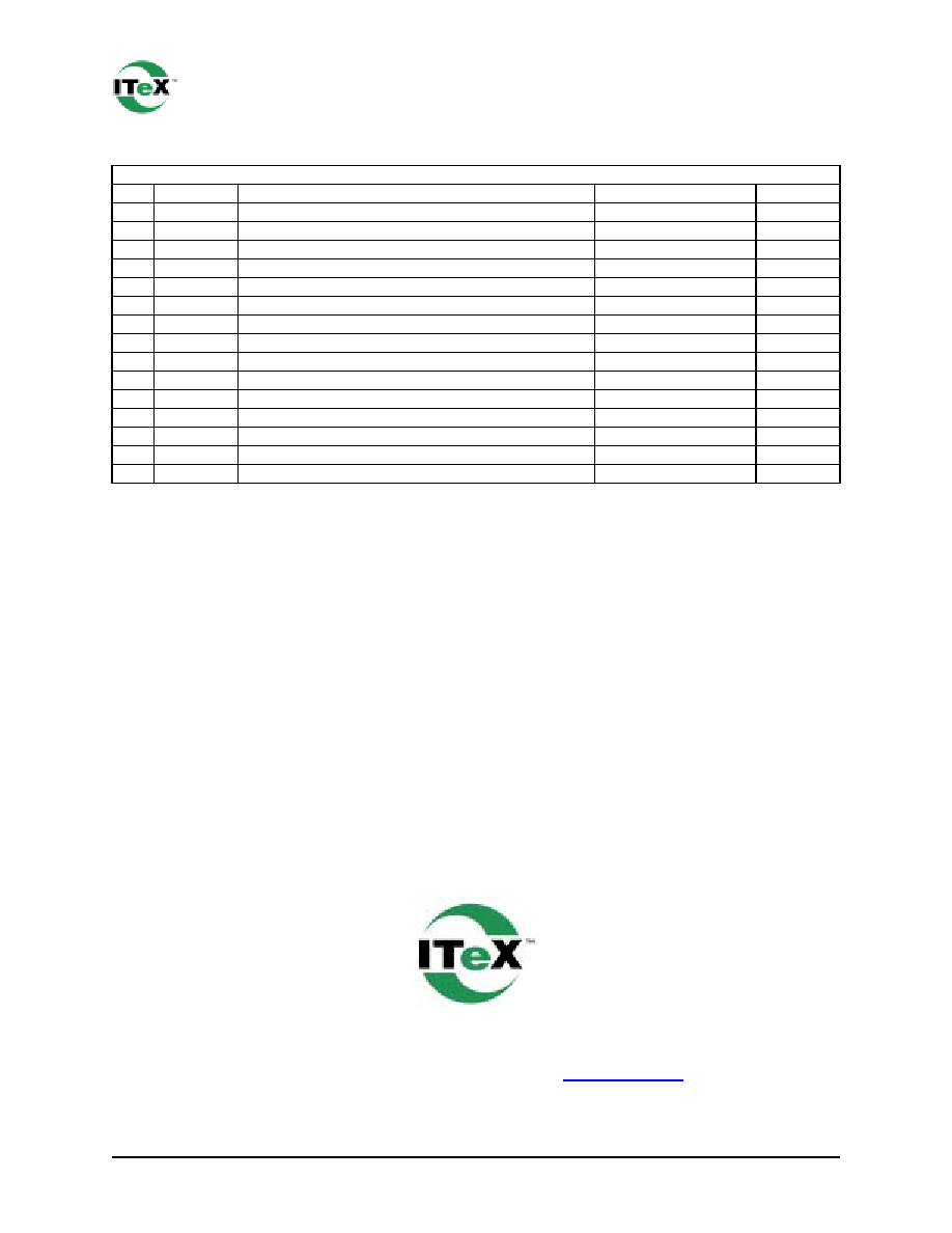
Pin
Name
Function
PCB Connection
Supply
Analog Interface
24
VRAP
positive voltage reference ADC
Decoupling network
AVDD3
25
VREF
ground reference ADC
Decoupling network
AVDD3
26
VRAN
negative voltage reference ADC
Decoupling network
AVDD3
29
NC
Not used
Decoupling network
AVDD4
30
NC
Not used
Decoupling network
AVDD4
31
TXP
pre driver output
Line driver input
AVDD4
32
TXN
pre driver output
Line driver input
AVDD4
38
AGND
virtual analog ground (AVDD/2=1.65V)
Decoupling network
AVDD5
44
VCOC
VCODAC time constant capacitor
VCODAC cap.
AVDD5
45
TSTCK
VCXO test mode setting pin
AVDD5
46
VCAP
VCXO mode setting pin
AVDD5
47
RXIN0
analog receive negative input Gain 0
Echo filter output
AVDD5
48
RXIP0
analog receive negative input Gain 0
Echo filter output
AVDD5
49
RXIN1
analog receive negative input Gain 1
Echo filter output
AVDD5
50
RXIP1
analog receive negative input Gain 1
Echo filter output
AVDD5
53
IREF
current reference TX DAC/DACE
Decoupling network
AVDD2
55
IVCO
current reference VCO DAC
VCO bias network
AVDD1
56
VCXO
VXCO control current
VCXO filter
AVDD1
59
XTALI
XTAL oscillator input pin
Crystal + varicap
AVDD1
60
XTALO
XTAL oscillator output pin
Crystal + varicap
AVDD1
Digital Interface
1
TX1
digital transmit input, parallel data
DVDD2
2
TX0
digital transmit input, parallel data
DVDD2
3
rev3
Only for testing
DVDD2
4
rev2
Only for testing
DVDD2
5
rev1
Only for testing
DVDD2
6
rev1
Only for testing
DVDD2
7
CTRLIN
serial data input (settings)
sync interface
DVDD2
9
CLKM
master clock output, f=35.328MHz
Load=CL<30pF
DVDD2
10
CLNIB
nibble clock output, f=17.664MHz (OSR=2) or
ground (OSR=4)
Load=CL<30pF
DVDD2
11
CLWD
word clock output, f=8.832/4.416MHz
Load=CL<30pF
DVDD2
12
RX3
digital receive output, parallel data
Load=CL<30pF
DVDD2
13
RX2
digital receive output, parallel data
Load=CL<30pF
DVDD2
14
RX1
digital receive output, parallel data
Load=CL<30pF
15
RX0
digital receive output, parallel data
Load=CL<30pF
DVDD2
18
PDOWN
power down select, "1"=power down
Power down input
DVDD2
19
LTNT
NT(ATU-R)//LT(ATU-C) select pin, NT=0/LT=1/test
mode MSB
VDD in ATU-C mode
DVDD2
20
RESETN
reset pin (active low)
RC-reset
DVDD2
22
GP0
General purpose output 0 (on AVDD 1)
Echo filter output
AVDD
33
GP1
General purpose output 0 (on AVDD 1)
Echo filter output
AVDD
43
GP2
General purpose output 0 (on AVDD 1)
Echo filter output
AVDD
63
TX3
digital transmit input, parallel data
Load=CL<30pF
DVDD2
64
TX2
digital transmit input, parallel data
Load=CL<30pF
DVDD2
57
XTAL
bypass
DC coupling for XTAL
AVSS
AVDD1
i80234 Product Specification
©
Integrated Telecom Express, Inc. Preliminary Specification, Confidential and Proprietary, Subject to Change Without Notice
6
Supply Voltages
8
DVSS1
DVSS
16
DVDD1
digital I/O supply voltage
DVDD
17
DVDD2
digital internal supply voltage
DVDD
23
AVSS3
AVSS
27
AVDD3
ADC supply voltage
AVDD
28
AVDD4
TX pre-drivers supply
AVSS
34
AVSS4
AVSS
35
AVSS5
AVSS
41
AVDD5
CT filter supply
AVDD
42
AVDD6
LNA supply
AVDD
51
AVSS6
AVSS
52
AVSS2
AVSS
54
AVDD2
DAC and support circuit
AVDD
58
AVDD1
XTAL oscillator supply voltage
AVDD
61
AVSS1
AVSS
62
DVSS2
DVSS
Integrated Telecom Express, Inc
2710 Walsh Avenue - Santa Clara, CA 95051 USA
"
1-408-980-8689
!
!
!
!
1-408-980-8831
www.itexadsl.com
Copyright © 1999-2000 Integrated Telecom Express, Inc.
All product names are trademarks or registered trademarks of their respective companies.
Specifications subject to change without notice.