 | –≠–ª–µ–∫—Ç—Ä–æ–Ω–Ω—ã–π –∫–æ–º–ø–æ–Ω–µ–Ω—Ç: ICM532B | –°–∫–∞—á–∞—Ç—å:  PDF PDF  ZIP ZIP |

ICM532B CIF Color CMOS Sensor with USB Output
Data Sheet, V 1.1 November, 2002
©2000, 2001,2002 IC Media Corporation & IC Media Technology Corp
11/21/2002
page 1
Company
Confidential
ICM532B
CIF Color CMOS Image Sensor
With USB Output
Data Sheet
V1.1
November, 2002
IC Media Corporation
545 East Brokaw Road
San Jose, CA 95112, U.S.A.
Phone: (408) 451-8838
Fax: (408) 451-8839
Email: Sales@IC-Media.Com
Web Site:
www.ic-media.com
IC Media Technology Corporation
6F, No. 61, ChowTze Street., NeiHu District
Taipei, Taiwan, R.O.C.
Phone: 886-2-2657-7898
Fax: 886-2-2657-8751
Email: Ap.Sales@IC-Media.Com.tw
Web Site: www.ic-media.com.tw
Important notice: This document contains information on a new product. IC Media Corp reserves the right to
make any changes without further notice to any product herein to improve design, function or quality and
reliability. No responsibility is assumed by IC Media Corp for its use, nor for any infringements of patents of
third parties, which may result from its use.

ICM532B CIF Color CMOS Sensor with USB Output
Data Sheet, V 1.1 November, 2002
©2000, 2001,2002 IC Media Corporation & IC Media Technology Corp
11/21/2002
page 2
Company
Confidential
Features
∑ CIF format (352x288) pixels, used with 1/7" optical system.
∑ QVGA format (320x240) pixels, used with 1/7" optical system
∑ QCIF format (176x144) pixels, cropped or subsampled, up to 37.5 fps.
∑ Progressive readout
∑ Output data format: compressed 8-bit raw data
∑ Image processing and decompression supported with proprietary software. Image processing functions
include color interpolation, color correction, auto white balance, auto exposure, auto anti-flickering, and
sharpening.
∑ Proprietary data compression
∑ Input/Output interface: USB 1.1 Full Speed
∑ Electronic exposure control
∑ On-chip 9-bit ADC
∑ Correlated double sampling
∑ Dead pixel and dead column removal
∑ Power down/Suspend mode
∑ 8 User Programmable GPIO pins
∑ Optional 3.3V Serial EEPROM register loading during power-up (24C02/04/08/16)
∑ Automatic optical black compensation
∑ Mirror image
∑ Single 3.3 V power supply
Key Parameters
∑ Number of Active Pixels: up to 352x288
∑ Number of Physical Pixels: 362x298
∑ Frame Rate: up to 30 fps ( 35 fps QCIF )
∑ Pixel Size: 6.0 µm x 6.0 µm
∑ Sensor Area: 2.2 mm x 1.8 mm
∑ Single Crystal Frequency: 6 MHz
∑ Exposure Time: 125 µs (@ 25 fps, 1 line) ~ 8 s (@ 12 fps)
∑ Sensitivity: 1.0 V/lux-sec (555 nm)
∑ Quantum Efficiency: 38 % (555 nm)
∑ Dynamic Range: 53 dB (analog), 48 dB (digital)
∑ Fill Factor: 36%
∑ S/N Ratio: 45 dB @ 75% full signal level
∑ Sensitive to infrared illumination source
∑ Digital Gain: 1 ~ 64 x @ 2
N
for all pixels
∑ RGB Gain: 1/256 ~ 64 x for individual Bayer pattern pixels
∑ Power Supply: 3.3 V
∑ Power consumption: 130mW typ.
∑ Packages: SPLCC48

ICM532B CIF Color CMOS Sensor with USB Output
Data Sheet, V 1.1 November, 2002
©2000, 2001,2002 IC Media Corporation & IC Media Technology Corp
11/21/2002
page 3
Company
Confidential
General Description
ICM-532B is a single-chip, CIF resolution, digital color PC camera with integrated data compression, line
buffer and Full Speed USB 1.1 interface. All the image processing functions (color interpolation, color
correction, auto white balance, auto exposure, auto anti-flickering, sharpening) are performed by software in
the host computer. It incorporates a 352x288 sensor array operating at 6 ~ 30 frames per second in
progressive manner. Each pixel is covered by a color filter, which forms a "Bayer pattern." Correlated
double sampling is performed by the internal ADC and timing circuitry. The raw data can be adjusted with
digital gain. The raw data is compressed using a proprietary compression scheme. The compression allows
video out in 8-bit compressed data format through USB 1.1 with 30 frames per second video capability. For
higher frame-rates, sub-sampled or cropped QCIF (176x144) modes are available that support 35 frames per
second.
8 Pins are supplied that can be programmed by the driver as general purpose I/O pins, with individually
selectable output enables. During power-up, the internal control registers can be loaded from an external
serial EEPROM. This allows customization of Vendor ID and Product ID, as well as initialization of other
device parameters.
The 48 MHz clock required for the ICM-532B is provided by an on-chip phase-lock loop that is driven by an
external 6 MHz crystal oscillator. Using a PLL reduces power dissipation, electrical noise and the cost of the
crystal. It also reduces the need for EMI shielding that would be required if a 48 MHz oscillator were used.
The highest frequency external signal is the 12Mbps on the differential USB data pins.
Software Support
∑ Computer & OS requirements: 750 MHz, 64M memory for 30 fps; 300 MHz, 64M memory for 12 fps.
Windows 98, Windows ME, Windows 2000
Macintosh OS 9.
∑ Driver support
∑ WDM USB driver
∑ TWAIN
∑ DirectShow
∑ VFW extension driver
∑ Proprietary DirectShow decoder
∑ Installation software
Applications
∑ PC camera
∑ Embedded Solutions (Notebooks, LCD monitors)
ICM532B CIF Color CMOS Sensor with USB Output
Data Sheet, V 1.1 November, 2002
©2000, 2001,2002 IC Media Corporation & IC Media Technology Corp
11/21/2002
page 4
Company
Confidential
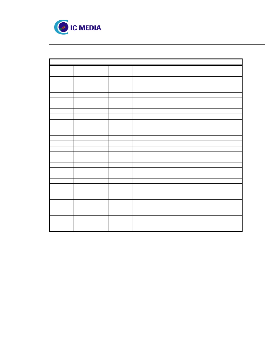
1. Pin
Assignments
Pin #
Name
Class
Function
36
DN
B,IO
USB D- connection
37
DP
B,IO
USB D+ connection
40
XIN
A,I
6 MHz Crystal Input
39
XOUT
A,O
6 MHz Crystal Output
3,5,34 Reserved D,O Leave
Unconnected
44
Test
D, I, N
Leave Unconnected
2
Clock_S
D, IO
Serial clock, for external serial EEPROM
1
Data_S
D, IO
Serial data, for external serial EEPROM
16 RSET A,I Resistor to Ground = 75
8
RSTN
D,SI,U
Chip Reset, active low
15 RAMP A,O
Analog
Test
Output
46
GPIO 0
D,IO
User Programmable I/O, Requires External Pull-up
47
GPIO 1
D,IO
User Programmable I/O, Requires External Resistor
48
GPIO 2
D,IO
User Programmable I/O, Requires External Pull-up
10
GPIO 3
D,IO
User Programmable I/O
11
GPIO 4
D,IO
User Programmable I/O
12
GPIO 5
D,IO
User Programmable I/O
13
GPIO 6
D,IO
User Programmable I/O
14
GPIO 7
D,IO
User Programmable I/O
7,27,31
VDDA
P
Sensor & PLL Analog Power
9,28,30
GNDA
P
Sensor & PLL Analog Ground
19
VDDD
P
Sensor Digital Power
17
GNDD
P
Sensor Digital Ground
4,26,33,
38,41,43
VDDK P Digital
Power
6,29,32,
35,42,45
GNDK P Digital
Ground
18 GNDS P Substrate
Ground
Class Code: A ≠ Analog signal, D ≠ Digital signal, I ≠ Input, SI ≠ Schmitt Input, O ≠ Output, IO ≠ Bidirectional, P ≠ Power or
ground, U ≠ Internal pull-up, N ≠ Internal pull-down, B ≠ USB Pad
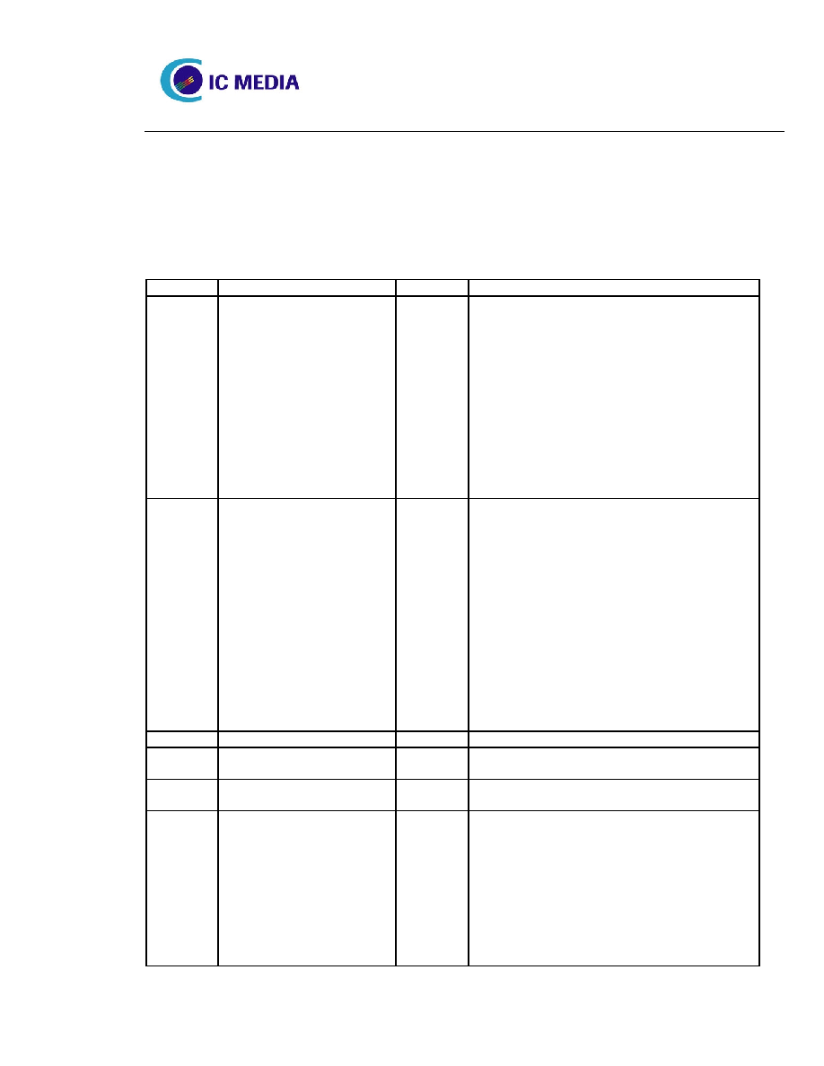
2. Functional Description
ICM-532B is a single-chip USB digital color imaging device. It includes a 352x288 sensor array, 352
column≠level ADC, and correlated double sampling circuitry. All the programmable parameters are set
by writing through the USB interface which can address the register file consisting of 8-bit registers.
The internal CIF image sensor is based upon the ICM-102B. The output format is USB 1.1 compatible
compressed video data using a single ISOCHRONOUS channel. Dead pixels and dead columns are

ICM532B CIF Color CMOS Sensor with USB Output
Data Sheet, V 1.1 November, 2002
©2000, 2001,2002 IC Media Corporation & IC Media Technology Corp
11/21/2002
page 5
Company
Confidential
removed, to generate a high quality image.
Figure 1. Block Diagram
2.1. Image Array
The image array consists of 352x288 pixels. Each pixel has a light sensitive photo diode and a set of
control and transfer transistors. At the beginning of the cycle, a row of pixels is pre-charged to its
maximum value. Then they are exposed to light for several lines worth of time and sampled by the
ADC. Correlated double sampling (CDS) is performed by subtracting the reset value (sampled right
before sampling the signal) from the signal value. The purpose of CDS is to eliminate the point-wise
fixed pattern noise (FPN). The output of CDS is approximately proportional to the amount of received
light, ranging from 0 to 255.
2.2. Color Filter
Each pixel is covered by a color filter. They form the Bayer Pattern as shown in Figure 2. (Row 0,
Column 0) is covered by a Red filter, (Row 0, Column 1) and (Row 1, Column 0) by Green filters, and
(Row 1, Column 1) by a Blue filter. Since each pixel only gets part of the frequency band, the data
needs further processing (i.e., color interpolation and color correction) in order to approximate the full
visible spectrum.
R
G
R
G
R
G
R
G
G
B
G
B
G
B
G
B
R
G
R
G
R
G
R
G
G
B
G
B
G
B
G
B
Figure 2. Color filter Bayer pattern
2.3. Exposure and Gain Control
The brightness of the scene may change by a great amount that renders the captured image either
ICM-102B
CIF Image
Sensor
5X Proprietary
Compression
Line Buffer
USB
1/7"
lens
USB Enabled
Computer

ICM532B CIF Color CMOS Sensor with USB Output
Data Sheet, V 1.1 November, 2002
©2000, 2001,2002 IC Media Corporation & IC Media Technology Corp
11/21/2002
page 6
Company
Confidential
over-exposed or under-exposed. To accommodate for different brightness, the user may change the
exposure time or digital gain by adjusting the AD_EXPOSE_TIMEH and AD_EXPOSE_TIMEL. The
exposure time is measured in terms of the time to read out one line of data, which is equal to 125 us
(assuming the line length is 500). If the number of lines per frame is set at 320 (the default), the
exposure time can vary from 1 to 319 lines. In addition, the user can adjust bit 7 to 5 of register
AD_EXPOSE_TIMEH to digitally boost the output value by 1 to 64 times @ 2N for all pixels.
Furthermore, users can adjust registers AD_M1_L, AD_M1_H, AD_M2_L, AD_M2_H, AD_M3_L,
AD_M3_H, AD_M4_L, AD_M4_H, to optimize the RGB gain (from 1/256 to 64) of the 4 Bayer
pattern pixels separately.
2.4. Output Format
During normal operation, the output format is 8-bit compressed data that ranges from 0 to 255. This
data is transmitted with a USB Transceiver using Isochronous packets. The video quality is related to
the size of the packets, with 1023 bytes/packet generating the highest quality image. The packets are
received, decompressed, and color processed by a host PC. A typical configuration is to connect
ICM-532B to a USB enabled PC. When operated at 24 fps CIF, the USB clock is 48 MHz and the Video
data clock is 4MHz. When operated at 30 fp, the Video data clock is 6MHz. The line and frame timing
can be adjusted through registers AD_WIDTH and AD_HEIGHT.
3. Control Registers
Registers may be configured using either the USB Command/Control Channel, or the Serial interface.
The result is unpredictable if both interfaces are used simultaneously. USB access should be made
using a Standard Vendor Type Device Request. For a write, if the Length field value is 0, the two bytes
in the Value field are written into two registers starting at the Index field value. For all other Length
field values, the data stage transfers the requested number of bytes starting from the Index field value.
The data transfer Length must not be larger than 8 bytes.
The 7-bit Serial ICM-532B device address is 0x21. ICM-532B can operate in either Serial master mode
or slave mode right after power up, depending on the pull-up or pull-down of the GPIO[1] pin. When
GPIO[1] is pulled low during power-up, ICM-102B's Serial interface is operated as a slave device,
waiting to be controlled by an external master such as a microprocessor. When GPIO[1] is pulled high
ICM532B CIF Color CMOS Sensor with USB Output
Data Sheet, V 1.1 November, 2002
©2000, 2001,2002 IC Media Corporation & IC Media Technology Corp
11/21/2002
page 7
Company
Confidential
during power-up, the Serial interface will first act as a master device, trying to read from an external
EEPROM (24C02/04/08/16). The first word read will indicate the number of bytes to transfer from the
external EEPROM. After transferring these bytes, or failing to access an external device, the
ICM-532B will behave like a slave device. The external EEPROM is addressed at address 0x50, and
must be 3.3v compatible.
Address Name
Default Description
0:00h PART_CONTROL
0
Processing
control
[0] 0: normal mode
[1] Slope adjustment enable
[2] Exposure time control, writing a 1 will activate
the new value set in AD_EXPOSE_TIME, when
read back from it, 0 means the exposure time
change is finished, 1 means the exposure time
change is still in progress.
[6:3] Reserved
[7] Latent change, writing a 1 means the changed
latent registers now starts taking effect, when the
entire operation is done, the read back value of this
bit will change from 1 to 0.
1:01h
2:02h
TIMING_CONTROL_LOW
TIMING_CONTROL_HIGH
17
0x0011
Timing control
[0] Column count enable, set to 0 when filling wave
table, set to 1 when normal operation
[3] Auto dark correction enable
[4] Timing select, 0: wave table timing, 1: default
timing
[8] IRST select, 0: from wave table, 1: from
IRST_NUMBER register
[11] Dead column removal mode, 0: color, 1:
black-and-white
[12] Out-of-array exposure pointer control, 0: point
to row 295, 1: point to row 298 (a non-existent row)
[13] Column stop, 0: sensor column counter stop at
361 when exceeding real array, 1: sensor column
counter keeps counting
7:07h TABLE_LEN
0
Reserved
12:0Ch
13:0Dh
AD_WIDTHL
AD_WIDTHH
500
0x01F4
[9:0] Frame width
14:0Eh
15:0Fh
AD_HEIGHTL
AD_HEIGHTH
400
0x0190
[15:0] Frame height, should not be less than
AD_ROW_BEGIN + 298
16:10h
17:11h
AD_COL_BEGINL
AD_COL_BEGINH
180
0x00B4
[9:0] Beginning of active line in terms of column
position
[10] Mirror image enable
[15:13] Digital gain
0: 1
1: 2
2: 4
3: 8
4: 16
5: 32
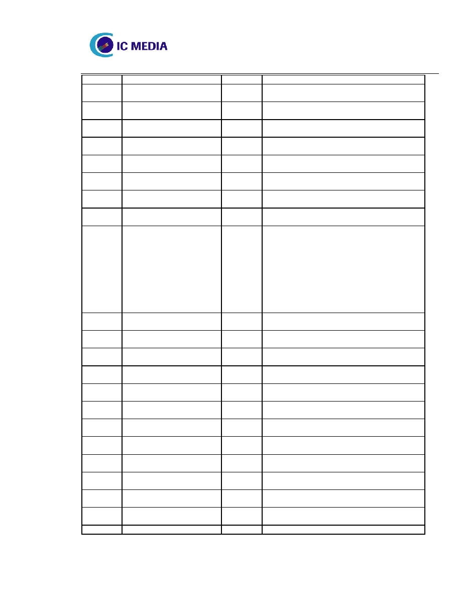
ICM532B CIF Color CMOS Sensor with USB Output
Data Sheet, V 1.1 November, 2002
©2000, 2001,2002 IC Media Corporation & IC Media Technology Corp
11/21/2002
page 8
Company
Confidential
6: 64
20:14h
21:15h
AD_ROW_BEGINL
AD_ROW_BEGINH
10
0x000A
[15:0] Beginning of active frame in terms of row
position
24:18h
25:19h
AD_HSYNC_ENDL
AD_HSYNC_ENDH
64
0x0040
[9:0] End of horizontal sync in terms of column
position
26:1Ah
27:1Bh
AD_VSYNC_ENDL
AD_VSYNC_ENDH
3
0x0003
[15:0] End of vertical sync in terms of row position
28:1Ch
29:1Dh
AD_EXPOSE_TIMEL
AD_EXPOSE_TIMEH
524
0x020C
[15:0] Exposure time in terms of number of rows
32:20h
33:21h
AD_M1_L
AD_M1_H
256
0x100
[10:0] Gain coefficient (G1), in unsigned 3.8 ~ 6.5
format (Selected by register 52)
34:22h
35:23h
AD_M2_L
AD_M2_H
256
0x100
[10:0] Gain coefficient (R), in unsigned 3.8 ~ 6.5
format (Selected by register 52)
36:24h
37:25h
AD_M3_L
AD_M3_H
256
0x100
[10:0] Gain coefficient (B), in unsigned 3.8 ~ 6.5
format (Selected by register 52)
38:26h
39:27h
AD_M4_L
AD_M4_H
256
0x100
[10:0] Gain coefficient (G2), in unsigned 3.8 ~ 6.5
format (Selected by register 52)
82:52h
AD_INOUTSEL
0
[4:0] Output format
0-7, 12-31: 8-bit raw data, with
0: RGB gain format = 3.8
1: RGB gain format = 4.7
2: RGB gain format = 5.6
3-7, 12-31: RGB gain format = 6.5
8: control signals
9: row address
10: column address
11: sensor raw data
110:6Eh
111:6Fh
AD_DEAD0L
AD_DEAD0H
1023
0x03FF
[9:0] Dead column #0 in terms of real sensor array
112:70h
113:71h
AD_DEAD1L
AD_DEAD1H
1023
0x03FF
[9:0] Dead column #1 in terms of real sensor array
114:72h
115:73h
AD_DEAD2L
AD_DEAD2H
1023
0x03FF
[9:0] Dead column #2 in terms of real sensor array
116:74h
117:75h
AD_DEAD3L
AD_DEAD3H
1023
0x03FF
[9:0] Dead column #3 in terms of real sensor array
118:76h
119:77h
AD_DEAD4L
AD_DEAD4H
1023
0x03FF
[9:0] Dead column #4 in terms of real sensor array
120:78h
121:79h
AD_DEAD5L
AD_DEAD5H
1023
0x03FF
[9:0] Dead column #5 in terms of real sensor array
122:7Ah
123:7Bh
AD_DEAD6L
AD_DEAD6H
1023
0x03FF
[9:0] Dead column #6 in terms of real sensor array
124:7Ch
125:7Dh
AD_DEAD7L
AD_DEAD7H
1023
0x03FF
[9:0] Dead column #7 in terms of real sensor array
126:7Eh
127:7Fh
AD_DEAD8L
AD_DEAD8H
1023
0x03FF
[9:0] Dead column #8 in terms of real sensor array
128:80h
129:81h
AD_DEAD9L
AD_DEAD9H
1023
0x03FF
[9:0] Dead column #9 in terms of real sensor array
130:82h
131:83h
AD_IDL
AD_IDH
54048
0xD320
[15:4] Device ID, can be programmed
144:90h
AD_DARK_DATA
0
[7:0] When auto dark correction is disabled, serve
as the subtrahend for dark correction
149:95h
AD_SLOPE_END_TIMEL
341
[9:0] When auto slope adjustment is turned on, if

ICM532B CIF Color CMOS Sensor with USB Output
Data Sheet, V 1.1 November, 2002
©2000, 2001,2002 IC Media Corporation & IC Media Technology Corp
11/21/2002
page 9
Company
Confidential
150:96h
AD_SLOPE_END_TIMEH
0x0155
the slope counter exceeds this value, the ramp will
become steeper
151:97h
152:98h
AD_WT_BEGINL
AD_WT_BEGINH
0 Reserved
153:99h
154:9Ah
AD_WT_ENDL
AD_WT_ENDH
1020
0x03FC
Reserved
155:9Bh
156:9Ch
AD_SUB_EN_TIMEL
AD_SUB_EN_TIMEH
474
0x01DA
[9:0] Column position where the CDS subtraction
pulse is applied
161:A1h
162:A2h
AD_WIDTHL_C
AD_WIDTHH_C
500
0x01F4
Reserved
163:A3h
164:A4h
AD_HEIGHTL_C
AD_HEIGHTH_C
400
0x0190
Reserved
165:A5h
166:A6h
AD_COL_BEGINL_C
AD_COL_BEGINH_C
100
0x0064
Reserved
167:A7h
168:A8h
AD_ROW_BEGINL_C
AD_ROW_BEGINH_C
10
0x000A
Reserved
169:A9h
170:AAh
AD_HSYNC_ENDL_C
AD_HSYNC_ENDH_C
64
0x0040
Reserved
171:ABh
172:ACh
AD_VSYNC_ENDL_C
AD_VSYNC_ENDH_C
3
0x0003
Reserved
173:ADh AD_PART_CONTROL_C 6
0x06
Reserved
174:AEh
175:AFh
AD_WT_BEGINL_C
AD_WT_BEGINH_C
0 Reserved
176:B0h
177:B1h
AD_WT_ENDL_C
AD_WT_ENDH_C
1020
0x03FC
Reserved
∑ *These registers are updated at the next falling edge of VSYNC after register UPD is set. The
occurrence of the update is marked in the video output by clearing bit 7 of the packet header. i.e. 80
=> 00. This bit remains set until register UPD is cleared.
4. GPIO
4.1. General Purpose I/O pins
There are 8 pins that can be programmed by the user as general purpose Input/Output pins. Three of the
pins are required to have pull-up or pull-down resistors attached to select device functionality at the
rising edge of NRST.
1. Special
Purpose:
GPIO[0] Pull-up.
It is possible to configure this output as an active low power-down pin, driven by the USB
controller Suspend signal. When so configured, all external power except pins 4, 33, and 43 may be
removed while this pin is driven low.
It is also possible to configure this output as an active low power-on pin, connected to an
external LED. When so configured, an external LED with 8ma current limiting resistor will be on

ICM532B CIF Color CMOS Sensor with USB Output
Data Sheet, V 1.1 November, 2002
©2000, 2001,2002 IC Media Corporation & IC Media Technology Corp
11/21/2002
page 10
Company
Confidential
unless the device is in Suspend state.
GPIO[1] Pull-up.
To enable external Serial EEPROM for register loads, Pull-down to disable this feature.
GPIO[2] Pull-up.
To select crystal oscillator clock source. Required condition
2. General
Purpose:
The other 5 GPIO pins have no Pull-up/Pull-down requirements. All of these pins default to inputs at
device reset. If the pins are to remain unused, an external pull-up is recommended to prevent the inputs
from floating.
To use an external switch, use a pull-up, and connect the switch between the GPIO pin and ground, and
poll the selected pin in register 58. The pull-up will return a high value, and a switch event will return a
low value.
5. Programming
5.1. Special considerations
There are several registers that need to be correctly programmed for device operation. If custom Vendor
ID/Product ID values are required, these registers should be programmed by an external Serial
EEPROM before the USB controller accesses the part
. It is recommended that the Vendor ID and
Product ID registers be programmed first. This allows the correct values to be set before the USB
configuration after power-up. After that, the driver can look for a specific register value to indicate the
end of Serial programming. During the initialization phase, if an external EEPROM is used, care must
be taken by the driver to not accesses registers while the EEPROM is transferring data. The driver
software should delay an appropriate time before accessing the registers.
Expansion RAM:
To access the internal 256Byte expansion RAM, load the RAA register with the desired address, and
read or write the RAD register.
Device Programming:
The maximum size of a USB data transfer is 8 bytes. Transfers larger than this will not read/write the
correct data values.
6. Electrical Characteristics
6.1. DC Characteristics
Customization of the VID/PID is available at a cost for large volume orders.
ICM532B CIF Color CMOS Sensor with USB Output
Data Sheet, V 1.1 November, 2002
©2000, 2001,2002 IC Media Corporation & IC Media Technology Corp
11/21/2002
page 11
Company
Confidential
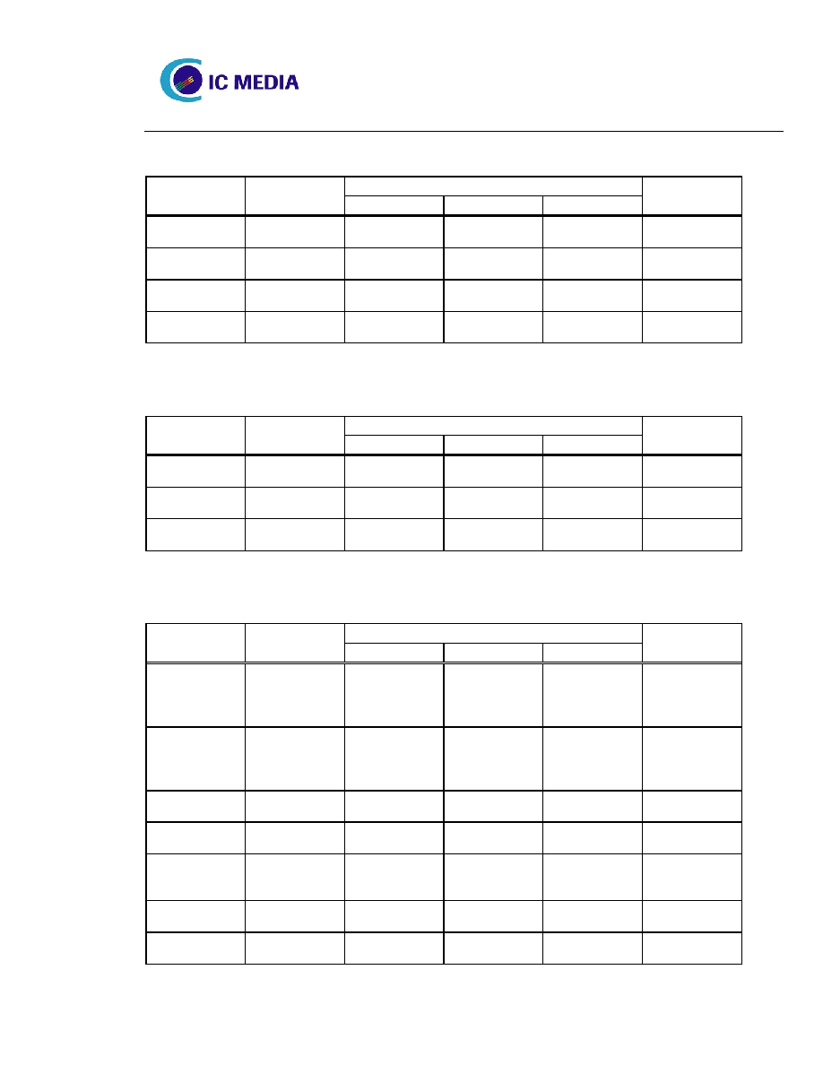
1. Absolute Maximum Ratings
Rating
Symbol Parameter
Minimum Typical Maximum
Units
V
CCA
Absolute
Power Supply
-0.3
3.8 V
V
INA
Absolute Input
Voltage
-0.3
V
CC
+ 0.3
V
V
OUTA
Absolute
Output Voltage
-0.3
V
CC
+ 0.3
V
T
STG
Storage
Temperature
0 25 65 ∞C
2. Recommended Operating Conditions
Rating
Symbol Parameter
Minimum Typical Maximum
Units
V
CC
Operating
Power Supply
3.0 3.3 3.6 V
V
IN
Operating
Input Voltage
0 V
CC
V
T
OPR
Operating
Temperature
0 25 55 ∞C
3. General DC Characteristics
Rating
Symbol Parameter
Minimum Typical Maximum
Units
I
DD
Operating
Current @
V
CC
=3.3 V, 25
∞C
40
mA
I
DDS
Suspend
Current @
V
CC
=3.3 V, 25
∞C
500
uA
I
IL
Input Low
Current
-1 1 µA
I
IH
Input High
Current
-1 1 µA
I
OZ
Tri-state
Leakage
Current
-10
10 µA
C
IN
Input
Capacitance
3 pF
C
OUT
Output
Capacitance
3 pF
ICM532B CIF Color CMOS Sensor with USB Output
Data Sheet, V 1.1 November, 2002
©2000, 2001,2002 IC Media Corporation & IC Media Technology Corp
11/21/2002
page 12
Company
Confidential
C
BID
Bi-directional
Buffer
Capacitance
3 pF
R
O
USB Output
Impedance
6 18
R
L
Input
Pull-up/down
Resistance
50
K
4. Electrical DC Characteristics
Rating
Symbol Parameter
Minimum Typical Maximum
Units
V
CC
Operating
Power Supply
3.0 3.3 3.6 V
V
OH
Output High
Voltage
2.4
V
V
UL
USB Output
Low Voltage
0.3
V
V
UH
USB Output
High Voltage
2.8
V
6.2. Clocking
The ICM-532B clock is generated from an external low cost 6MHz crystal. The on-board PLL
generates the required USB clock and the Video Clock. The nominal Video Clock rate is 8MHz. This
rate can be altered by setting either the Fastclock ( *1.5 ) or Slowclock ( /2.0 ) register bits.
Video Timing examples:
At 8MHz, the Video clock generates 1 pixel every 250ns, a line (500 pixels) every 125us, and 8 lines
every 1ms. This produces 8 lines to be packed into 1 USB data transfer, to make a 24 fps QVGA (352
x288) transfer rate.
At 12MHz, the Video clock generates 1 pixel every 166.7ns, a line (600 pixels) every 100us, and 10
lines every 1 ms. This produces 10 lines to be packed into 1 USB data transfer, to make a 30 fps QVGA
(320x240) transfer rate.
At 12MHz, the Video clock generates 1 pixel every 166.7ns, a line (500 pixels) every 83.3us, and 12
lines every 1 ms. This produces 6 lines to be packed into 1 USB data transfer, to make a 35 fps QCIF
(176 x 144) transfer rate.
ICM532B CIF Color CMOS Sensor with USB Output
Data Sheet, V 1.1 November, 2002
©2000, 2001,2002 IC Media Corporation & IC Media Technology Corp
11/21/2002
page 13
Company
Confidential
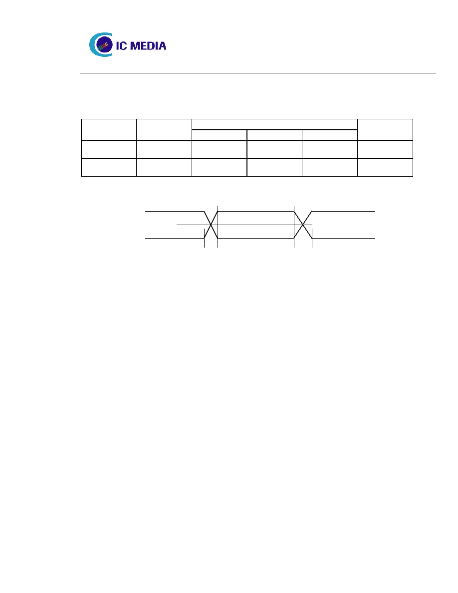
6.3. AC Characteristics
Rating
Symbol Parameter
Minimum Typical Maximum
Units
T
RISE/FALL
USB Switching
Times
4 10 20 ns
V
CR
USB Cross
Point
1.3
2.0 V
Figure 3. DP/DN Timing
T
RISE
T
FALL
V
CR
V
UL
V
UH
90%
10%
90%
10%
ICM532B CIF Color CMOS Sensor with USB Output
Data Sheet, V 1.1 November, 2002
©2000, 2001,2002 IC Media Corporation & IC Media Technology Corp
11/21/2002
page 14
Company
Confidential
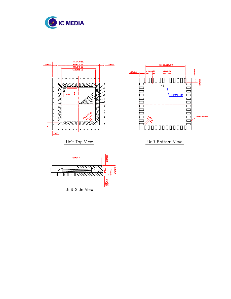
7. Mechanical Information
ICM532B supports SPLCC (
Plastic Shrunk LCC48 Packaging) packaging. Note that pin 1 should
point to the top of the camera when a lens and the default driver are used.
Figure 4. SPLCC48 Packaging
8. Board Design Information
Components:
∑ ICM-532B
∑ 6MHz Crystal
∑ RSET resistor
∑ USB connector or cable with 1.5k pull-up on DP.
∑ 3.3v voltage regulator and associated components
∑ Power Supply filter capacitors
∑ Pull-up for SDA, SCL, GPIO0 GPIO1, and GPIO2
∑ If desired: Reset circuitry. A 0.1uF capacitor on RSTN is sufficient for power-on reset.

ICM532B CIF Color CMOS Sensor with USB Output
Data Sheet, V 1.1 November, 2002
©2000, 2001,2002 IC Media Corporation & IC Media Technology Corp
11/21/2002
page 15
Company
Confidential
9. Ordering Information
Part number for different package:
Description Part
Number
Shrunk Plastic LCC48 package packaged, USB CIF resolution sensor (3.3 V)
ICM-532Bsa
Contact Addresses:
IC Media Corporation
545 East Brokaw Road
San Jose, CA 95112, U.S.A.
Phone: (408) 451-8838
Fax: (408) 451-8839
Email: Sales@IC-Media.Com
Web Site:
www.ic-media.com
IC Media Technology
6F, No. 61, ChowTze Street., NeiHu District
Taipei, Taiwan, R.O.C.
Phone: 886-2-2657-7898
Fax: 886-2-2657-8751
Email: Sales@IC-Media.Com
Web Site:
www.ic-media.com