 | –≠–ª–µ–∫—Ç—Ä–æ–Ω–Ω—ã–π –∫–æ–º–ø–æ–Ω–µ–Ω—Ç: ICS1702MT | –°–∫–∞—á–∞—Ç—å:  PDF PDF  ZIP ZIP |

ICS1702
QuickSaverÆ Charge Controller for Nickel-Cadmium
and Nickel-Metal Hydride Batteries
General Description
The ICS1702 is a CMOS device designed for the intelligent charge
control of either nickel-cadmium (NiCd) or nickel-metal hydride
(NiMH) batteries. The controller uses a pulsed-current charging
technique together with voltage slope and/or temperature slope
termination. The ICS1702 employs a four stage charge sequence
that provides a complete recharge with-out overcharging. The
controller has nine user-selectable charge rates and six user-
selectable auxiliary modes available for customized charging
systems.
The ICS1702 monitors for the presence of a battery and begins
charging when a battery is installed. Voltage and temperature are
measured to ensure a battery is within fast charge conditions before
charge is initiated.
Applications
Battery charging systems for:
-
Portable consumer electronics
-
Power tools
-
Audio/video equipment
-
Communications equipment
-
Portable medical electronics
-
Wireless handsets
Features
∑
Multiple charge termination methods include:
-
Voltage slope
-
Temperature slope
-
Maximum temperature
-
Charge timer
∑
Four stage charge sequence:
-
Soft start charge
-
Fast charge
-
Topping charge
-
Maintenance charge
∑
Reverse-pulse charging available in all charge stages
∑
Nine programmable charge rates between 15 minutes (4C) and
four hours (C/4)
∑
Out-of-temperature range detection
-
Hot battery: charger shutdown
-
Cold battery: low current charge
∑
Continuous polling mode for battery detection
∑
Six auxiliary modes include:
-
Discharge-before-charge
-
Ten hour C/10 conditioning charge
-
Direct to C/40 maintenance charge
-
Charging system test provided through controller
∑
Adjustable open circuit (no battery) voltage reference
Block Diagram
CHARGE
DISCHARGE
TEMPERATURE
SENSE
SELECT
CHARGE
VOLTAGE
SENSE
MODE SELECT
OPEN CIRCUIT
REFERENCE
PROCESSOR
MICROCODE CONTROL
ADC
RAM
ROM
OUTPUT
CONTROL
0.5V
HOT
COLD
RESET
TERMINATION
SELECT
TEMPERATURE
STATUS LED
CHARGE
MODE LED
MAINTENANCE
MODE LED
POLLING
MODE LED
CONTROL
CONTROL
RC
OSCILLATOR
QuickSaver
Æ
Æ
is a registered trademark of Galaxy Power, Inc
.

2
ICS1702
Pin Configuration
Pin Definitions
20-Pin DIP or SOIC
ICS1702
CHG
DCHG
PFN
CMN
MMN
VSS
AUX1
RC
THERM
OPREF
VIN
VDD
AVSS
OTN
SEL1
MRN
SEL0
AUX0
DTSEL
1
2
3
4
5
6
7
8
9
10
11
12
13
14
15
16
17
18
19
20
unused
Pin Number
Pin Name
Type
Definition
1
CHG
OUT
Active high TTL compatible signal used to turn on an external current source to provide current to charge
the battery.
2
DCHG
OUT
Active high TTL compatible signal available to turn on a discharge circuit.
3
PFN
OUT
Polling detect indicator. An active low turns on an external indicator to show the controller is polling for
the presence of the battery.
4
MMN
OUT
Maintenance mode indicator. An active low turns on an external indicator showing the battery is either in
the topping charge, maintenance charge or auxiliary condition mode. This signal is also applied with the
out-of-temperature range indicator when the controller is in a cold battery charge mode. The indicator
flashes during the auxiliary discharge mode.
5
CMN
OUT
Charge mode indicator. An active low turns on an external indicator to show the controller is either in a
soft start charge or fast charge.
6
OTN
OUT
Out-of-temperature range indicator. An active low turns on an external indicator showing the battery is
out of the normal fast charge temperature range.
7
SEL0
IN
Tri-level input used with the SEL1 pin to program the device for the desired charge rate.
8
VSS
Ground.
9
AVSS
Ground.
10
SEL1
IN
Tri-level input used with the SEL0 pin to program the device for the desired charge rate.
11
MRN
IN
Master reset signal. A logic low pulse greater than 700 ms initiates a device reset.
12
RC
IN
An external resistor and capacitor sets the frequency of the internal clock.
13
DTSEL
IN
Selects temperature slope and/or voltage slope termination.
14
AUX0
IN
Tri-level input used with the AUX1 pin to program the device for an auxiliary operating mode.
15
AUX1
IN
Tri-level input used with the AUX0 pin to program the device for an auxiliary operating mode.
16
THERM
IN
Thermistor or thermal switch input for temperature sensing.
17
OPREF
IN
Open circuit (no battery) voltage reference. An external resistor divider on this pin sets the open circuit
voltage reference used to detect the presence of a battery.
18
VIN
IN
Battery voltage normalized to one cell with an external resistor divider.
19
unused
Ground.
20
VDD
Device supply =+5.0 VDC
Note:
Pin 11 has an internal pull-up.
Pin 16 has an internal pull-up.
Pin 13 has an internal pull-down.
Pins 7, 10, 14, 15 float to 2.3V when unconnected.

3
ICS1702
Controller Operation
Charging Stages
The charging sequence consists of four stages. The application of
current is shown graphically in Figure 1. The soft start stage
gradually increases current levels up to the user selected fast
charge rate during the first two minutes. The soft start stage is
followed by the fast charge stage, which continues until
termination. After termination, a two hour C/10 topping charge is
applied. The topping charge is followed by a C/40 maintenance
charge.
Soft Start Charge
Some batteries may exhibit an unusual high impedance condition
while accepting the initial charging current, as shown in Figure 2.
Unless dealt with, this high impedance condition can cause a
voltage peak at the beginning of the charge cycle that would be
misinterpreted as a fully charged battery by the voltage termination
methods.
The soft start charge eases batteries into the fast charge stage by
gradually increasing the current to the selected fast charge rate. The
gradual increase in current alleviates the voltage peak. During this
stage, only positive current pulses are applied to the battery. The
duty cycle of the applied current is increased to the selected fast
charge rate, as shown in Figure 3, by extending the current pulse
on every cycle until the pulse is about one second in duration. The
initial current pulse is approximately 200ms. The CMN indicator is
activated continuously during this stage.
Figure 1: Graphical representation of average current levels during the four charging stages
Figure 2: High impedance voltage spike at the beginning of charge
S o ft- S ta rt
F as t C har ge
Topp in g C h ar ge
M ain te nan ce C ha rge
C u rr ent
Tim e (no t to s ca le)
(n ot to s c ale)
S tage 3
S ta ge 4
S tage 2
S tage 1
0
2 m in
te rm in ation
te rm in ation + 2 ho urs
A ve rag e
4
ICS1702
Figure 3: Cycle-to-cycle increase of the soft-start current pulse widths
The amplitude of the current pulse is determined by system
parameters such as the current capability of the charging system,
the desired charge rate, the cell capacity and the ability of that cell
to accept the charge current. The ICS1702 can be set for nine user-
selectable fast charge rates from 15 minutes (4C) to four hours
(C/4). Charge pulses occur approximately every second. The CMN
indicator is activated continuously during this stage.
Fast Charge
In the second stage, the ICS1702 applies the charging current in a
series of charge and discharge pulses. The technique consists of a
positive current charging pulse followed by a high current, short
duration discharge pulse. The cycle, shown with charge, discharge,
rest and data acquisition periods in Figure 4, repeats every second
until the batteries are fully charged.
Figure 4: Charge cycle showing charge and discharge current pulses
Initial Pulse
Width
cycle time
cycle time
cycle time
Initial Pulse
Width
Initial Pulse
Width
increment
time
2 x increment
time
fast charge pulse width
acquisition tim e
rest
time
rest
time
discharge puls e width
voltage
acquisition time
temperature
time
rest
cyc le time

5
ICS1702
The discharge current pulse amplitude is typically set to about 2.5
times the amplitude of the charging current based on 1.4V/cell. For
example, if the charge current is 4 amps, then the discharge current
is set at about 10 amps. The energy removed during the discharge
pulse is a fixed ratio to the positive charge rate. The amplitude of
the discharge pulse does not affect the operation of the part as
described in this section.
A voltage acquisition window immediately follows a brief rest time
after the discharge pulse. No charge is applied during the rest time
or during the acquisition window to allow the cell chemistry to
settle. Since no current is flowing, the measured cell voltage is not
obscured by any internal or external IR drops or distortions caused
by excess plate surface charge. The ICS1702 makes one
continuous reading of the no-load battery voltage during the entire
acquisition window. The voltage that is measured during this
window contains less noise and is a more accurate representation
of the true state of charge of the battery. If temperature termination
is selected, the thermistor voltage is sampled after a brief rest time
once the current supply to the battery is turned on.
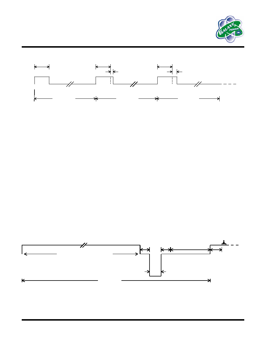
Topping Charge
The third stage is a topping charge that applies current at a rate low
enough to prevent cell heating but high enough to ensure a full
charge.
The topping charge applies a C/10 charging current for two hours.
The current consists of the same pulse technique used during the
fast charge stage; however, the duty cycle of the pulse sequence
has been extended as shown in Figure 5. Extending the time
between charge pulses allows the same charging current used in the
fast charge stage so that no changes to the current source are
necessary. For example, the same charge pulse that occurs every
second at a 2C fast charge rate will occur every 20 seconds for a
topping charge rate of C/10. The MMN indicator is activated
continuously during this stage.
Maintenance Charge
The maintenance charge is intended to offset the natural self-
discharge of NiCd or NiMH batteries by keeping the cells primed
at peak charge. After the topping charge ends, the ICS1702 begins
this charge stage by extending the duty cycle of the applied current
pulses to a C/40 rate. The maintenance charge will last for as long
as the battery voltage is greater than 0.5V at the VIN pin, or, if the
ten hour timer mode is enabled, until the timer stops the controller.
The MMN indicator is activated continuously during this stage.
Figure 5: Representative timing diagram for topping and maintenance charge
delay time
time
cycle
time
cycle

6
ICS1702
Cells that are not thoroughly conditioned or possess an unusual cell
construction may not have a normal voltage profile. The ICS1702
uses an alternate method of charge termination based on a slight
decrease in the voltage slope to stop charge to cells whose voltage
profile is very shallow. This method looks for a flattening of the
voltage slope which may indicate a shallow peak in the voltage
profile. The zero slope point occurs slightly beyond the peak
voltage and is shown on the voltage curve graph.
Charge Termination Methods
Several charge termination schemes, including voltage slope,
temperature slope, maximum temperature and two overall charge
timers are available. The voltage slope and negative voltage slope
methods may be used with or without the temperature slope and the
maximum temperature method. Maximum temperature and the fast
charge timer are available as backup methods.
Voltage Slope Termination
The most distinctive point on the voltage curve of a charging
battery in response to a constant current is the voltage peak that
occurs as the cell approaches full charge. By mathematically
calculating the first derivative of the voltage, a second curve can be
generated showing the change in voltage with respect to time as
shown in Figure 6. The slope will reach a maximum just before the
actual peak in the cell voltage. Using the voltage slope data, the
ICS1702 calculates the point of full charge and accurately
terminates the applied current as the battery reaches that point. The
actual termination point depends on the charging characteristics of
the particular battery.
Figure 6: Voltage and slope curves showing inflection and zero slope points

7
ICS1702
Figure 8: Cell temperature and
thermistor voltage slope
Table 1 shows the decrease in thermistor voltage the last minute
before full charge required by the ICS1702 at various charge rates.
The thermistor voltage slope should exceed the listed value to
ensure charge termination. Note that changes in thermistor
location, cell size or large ambient temperature fluctuations can
affect the slope to some degree. Refer to the Applications
Information section and Temperature Slope and Maximum
Temperature section for more information on thermistor mounting.
Table 1: Slope vs. Charge Rate
Temperature Slope Termination
Temperature slope termination is based on the battery producing an
accelerated rate of heating as the amount of readily chargeable
material dimishes at full charge. An increase in battery (cell)
heating due to the charging reaction will occur at a much faster rate
than a change due to a warming ambient temperature. Note the
effect of 0.5
∞
C fluctuations in ambient temperatures resulting in
slight variations in the temperature slope as shown in Figure 7.
However, the increase in cell temperature near the end of charge
causes a much larger change in the temperature slope that can be
easily detected and used as a trigger for fast charge termination.
Figure 7: Cell temperature and
temperature slope
The rate of change in cell temperature can be determined by
measuring the change in voltage across a negative temperature
coefficient thermistor as shown in Figure 8. The resistance of an
NTC thermistor changes in proportion in the change in temperature
of the thermistor. The ICS1702 measures the decreasing resistance
as a drop in voltage and calculates the thermistor voltage slope,
shown in Figure 8. The controller terminates fast charge based on
the selected charge rate and the calculated slope.
Charge Rate
Thermistor Voltage Slope
(-V/min.)
>C/2
0.040
C/2 to C/3
0.028
<C/3
0.018

8
ICS1702
If a thermal switch is used, a 45
∞
C open circuit switch is
recommended. When the thermal switch opens, an internal pull-up
at the THERM pin results in a logic high which shuts down the
controller and activates the OTN indicator. The controller must be
reset once the hot battery fault condition has cleared to restart the
charge sequence.
Maximum temperature termination can be disabled by grounding
the THERM pin. See the section on Temperature Sensing for more
information.
Fast Charge Timer Termination
The controller uses a timer to limit the fast charge duration.
These times are pre-programmed, and are automatically adjusted in
time duration according to the charge rate selected. Fast charge
timer termination is best suited as a safety backup feature to limit
the duration of the fast charge stage. The fast charge timer is
always enabled and cannot be disabled. See Table 4 in the section
Charge Rate Selection for more information.
To determine the required thermistor characteristics for proper
temperature slope termination, the battery temperature rise must be
known or determined for the last minute prior to full charge.
Maximum temperature termination is also enabled when
temperature slope termination is used. Care must be taken to keep
voltage levels at the THERM pin within the fast charge range
(between 2.4V and 0.93V), as shown in Figure 9.
Maximum Temperature Termination
Maximum temperature can be sensed using either a NTC
thermistor or a thermal switch. Maximum temperature termination
can also be bypassed if desired, although it is strongly
recommended that some form of temperature termination be used.
If an NTC thermistor is used, an internal voltage threshold
determines when the battery is too hot to charge. As temperature
increases, the voltage across the thermistor will drop. This voltage
is continually compared to the internal voltage threshold. If the
thermistor voltage drops below the internal threshold, the OTN
indicator is activated and the controller shuts down. The controller
must be reset once the hot battery fault condition has cleared to
restart the charge sequence.

9
ICS1702
Battery Detection
Upon power-up or after a master reset, excess charge from output
filter capacitors at the charging system terminals is removed with a
series of discharge pulses. After the discharge pulse sequence is
complete, the voltage at VIN must be greater than 0.5V when a
battery is present. If the voltage at the pin is less than 0.5V, the
ICS1702 assumes no battery is present, and the polling detect
mode is initiated. No indicator is active during the discharge
pulses.
The ICS1702 enters the polling detect mode and applies a
100ms charge pulse. During the pulse, the ICS1702 monitors the
VIN pin to determine if the divided down terminal voltage is above
OPREF. If the battery is present, the voltage will be clamped below
the reference on OPREF while the current pulse is applied. If a
battery is not present, the voltage at VIN will rise above the
reference at OPREF.
The charge pulse will repeat until the battery is reinstalled. The
polling detect indicator (PFN) is the only indicator active as long as
the ICS1702 is in the polling detect mode. Once a battery is
installed, the ICS1702 will turn off the PFN indicator and enter the
soft start stage. The ICS1702 will automatically reenter the polling
detect mode if the battery is removed.
Battery Removal
During the application of a charge pulse, the voltage at the VIN pin
is compared to the voltage at the OPREF pin. If the voltage at VIN
is greater than the voltage at OPREF during the application of the
current pulse, then the battery is assumed to have been removed
and the ICS1702 enters the polling detect mode. If the voltage at
VIN is below the voltage at OPREF, the charging mode continues.
When in the topping charge or maintenance charge stages, a charge
pulse may not occur for several seconds. During the period
between charge pulses, the voltage at VIN must be greater than
0.5V if a battery is attached. If the voltage at VIN is less than 0.5V,
the ICS1702 assumes the battery has been removed, and the
polling detect mode is initiated.
Auxiliary Modes of Operation
The ICS1702 allows six alternate modes of operation to help
customize the charging system for certain applications. The tri-
level AUX0 and AUX1 pins are used to select the operating mode.
The AUX0 and AUX1 pins default the ICS1702 into fast charge
operation. Except for the discharge-to-charge mode, another mode
can only be selected by re-programming and resetting the
controller.
Discharge-to-Charge Mode
The time required for discharge depends on the energy in the battery
and the discharge rate. The discharge is not limited by a timer. This
allows the user to set the discharge rate. The battery is drained to 1
volt/cell as read at the VIN pin under load and then the controller
enters soft start at a charge rate set by the SEL0 and SEL1 inputs. The
discharge load is activated by the DCHG pin which goes low for about
400ms every second. A resistor value selected for a 2.5C discharge
based on 1.4V/cell results in about a 1C discharge rate.
The discharge-to-charge mode can be entered by placing the
AUX0 pin high (H) and the AUX1 pin low (L) with the SEL0 and
SEL1 inputs set for the desired fast charge rate. This setting initializes
the discharge sequence. The ICS1702 enters the discharge-to-charge
mode at initial power-up or with a master reset. The discharge mode
occurs first, to be followed by the selected fast charge mode. During
discharge, the MMN indicator flashes at a one second rate, while
during the soft start and fast charge stages the CMN indicator is
activated continuously.
Four charge modes are available after the discharge portion is complete
by changing the state of the AUX inputs during the discharge portion
of this mode. The available charge modes are:
∑
Fast Charge: Leave the AUX inputs open (Z).
∑
Direct Maintenance Mode: Set the AUX0 low (L) and AUX1 high
(H).
∑
Condition Mode: Set AUX0 high (H) and AUX1
∑
open (Z).
∑
Ten-Hour Timer Mode: Set AUX0 high (H) and AUX1 high (H).
If the battery is removed while in the discharge-to-charge mode, the
ICS1702 will continually reset itself until the battery is reinstalled. See
Application Information for more information.
Discharge-Only Mode
The time required for discharge depends on the energy in the battery
and the discharge rate. The discharge is not limited by a timer. This
allows the user to set the discharge rate. The battery is drained to 1
volt/cell as read at the VIN pin under load. The ICS1702 shuts down
after the discharge sequence is finished and a master reset must be
performed to reactivate the device. The discharge load is activated by
the DCHG pin which goes low for about 400ms every second. A
resistor value selected for a 2.5C discharge based on 1.4V/cell results
in about a 1C discharge rate. The discharge-only mode can be entered
by placing the AUX0 pin open (Z) and the AUX1 pin low (L). The
ICS1702 enters this mode at initial power-up or with a master reset.
During the discharge portion, the MMN indicator flashes at a one
second rate.

10
ICS1702
Charging System Test
The system test mode is intended for use in applications where the
charging system functionality needs to be tested. The system test
sequence consists of a one second activation of the CMN, MMN
and PFN indicator pins as well as the CHG and DCHG lines. The
OTN indicator is not activated. The system test mode is entered by
placing both the AUX0 and AUX1 pins low (L). The ICS1702
shuts down after the test sequence is finished and a master reset
must be performed to reactivate the device.
Cold Battery Charging
Cold battery charging is activated if a voltage at the THERM pin is
in the cold battery voltage range, as shown in Figure 9. The
ICS1702 checks for a cold battery before initiating fast charge. If a
cold battery is present before fast charge begins, the ICS1702
begins a two-hour C/10 topping charge (the pulsed duty cycle is
based on the selected charge rate). If the battery is still cold after
the two hour topping charge is complete, the ICS1702 begins a
C/40 maintenance charge. The maintenance charge will continue
for as long as the battery remains cold Unless the ten hour time
mode is selected. The thermistor voltage at the THERM pin is
checked every second to see if the battery has warmed up. If so, the
ICS1702 stops the topping or maintenance charge and begins a fast
charge at a rate selected by the SEL0 and SEL1 inputs. A cold
battery does not interfere with the condition mode, direct
maintenance mode, the discharge portion of the discharge-to-
charge mode, or the discharge-only mode as programmed by the
AUX0 and AUX1 pins. See the section on Temperature Sensing,
for more information.
The MMN and OTN indicators will be active, indicating that a low
current charge is being applied to a battery that is outside the
specified temperature range for fast charging. If the CMN and
OTN indicators are active see the Application Information section.
Direct Maintenance Mode
The ICS1702 can enter directly into the C/40 maintenance mode
for cells that require a maintenance charge only. The direct
maintenance mode is activated by setting the AUX0 pin low (L)
and the AUX1 pin high (H), and resetting the device. The SEL0
and SEL1 pins must be set based on the charging current and the
battery capacity. The formula
Charging Current (Amps)
Battery Capacity (Amp
∑
hr)
gives the charge rate. Use Table 4 to find the correct SEL0 and
SEL1 settings. The maintenance charge is applied until the battery
is removed, upon which the ICS1702 will enter the polling detect
mode. The ICS1702 will enter the direct maintenance mode upon
initial power-up or after a master reset. The MMN indicator will be
active during this mode.
Conditioning Mode
The ICS1702 can enter a conditioning mode which applies a C/10
charge for a timed 10 hour period, followed by an indefinite C/40
maintenance charge until the batteries are removed.
The conditioning mode can be entered by setting the AUX0 pin
high (H) and the AUX1 pin open (Z). The SEL0 and SEL1 pins
must be set based on the charging current and the battery capacity.
The formula
Charging Current (Amps)
Battery Capacity (Amp
∑
hr)
gives the charge rate. Use Table 4 to find the correct SEL0 and
SEL1 settings. The MMN indicator will be active during the 10
hour conditioning charge and the maintenance charge that follows.
The ICS1702 enters the polling detect mode if the battery is
removed.
Ten Hour Timer Mode
Placing the AUX0 and AUX1 pins both high (H) enables a ten
hour timer. This timer limits the total charge, including the
maintenance charge, to approximately ten hours for a battery that is
completely discharged before fast charge is initiated. The ten hour
limit is based on the assumption that the charge terminates due to
the fast charge timer as shown in Table 2
Table 2: Ten Hour Timer Information
Charge Rate
Fast Charge Timer Cutoff
Maintenance Timer Cutoff
(after fast charge termination)
Charge Time Limit
(from reset)
4 C
0.3 hrs
9.7 hrs
10 hrs
2 C
0.6 hrs
9.4 hrs
10 hrs
1.3 C
0.9 hrs
9.1 hrs
10 hrs
1 C
1.2 hrs
8.8 hrs
10 hrs
C/1.5
1.8 hrs
8.2 hrs
10 hrs
C/2
2.4 hrs
7.6 hrs
10 hrs
C/2.5
3.5 hrs
6.5 hrs
10 hrs
C/3
4.0 hrs
6.0 hrs
10 hrs
C/4
4.6 hrs
5.4 hrs
10 hrs

11
ICS1702
The maintenance mode (MMN) indicator is on when the ICS1702
is either in the topping charge, maintenance charge, direct
maintenance mode, or the condition mode. The MMN indicator is
also lit in conjunction with the OTN indicator when cold battery
charging is in progress. The maintenance mode indicator flashes at
a one second rate when the ICS1702 is controlling the discharge
portion of the discharge-to-charge or the discharge-only mode.
The polling detect (PFN) indicator is on when the ICS1702 polls
for a battery. The controller applies periodic charge pulses to detect
the presence of a battery. The indicator is a warning that these
charge pulses are appearing at the charging system terminals at
regular intervals. When a battery is detected, the indicator is turned
off.
The out-of-temperature range (OTN) indicator is active whenever
the voltage at the temperature sense (THERM) input enters a range
that indicates that the attached battery is too hot to charge. The
OTN indicator is also activated with the MMN indicator if the
controller is initialized with the battery in the cold battery charge
region.
Charge Rate Selection: SEL0, SEL1 Pins
The SEL0 and SEL1 inputs must be programmed by the user to
inform the ICS1702 of the desired charge rate. When left
unconnected (open), these tri-level pins will float to about 2.3V.
When a low level is required, the pin must be grounded. When a
high level is required, the pin must be tied to V
DD
. The voltage
ranges for low (L), open (Z) and high (H) are listed in Table 10,
DC Characteristics. To program the SEL0 and SEL1 inputs, refer
to the Charge Rate List in Table 4.
The ICS1702 does not control the current flowing into the battery
in any way other than turning it on and off. The required current
for the selected charge rate must be provided by the user's power
source. The external charging circuitry should provide current at
the selected charge rate. For example, to charge a 1.2 ampere hour
battery in 30 minutes (2C), approximately 2.4 amperes of current is
required.
Pin Descriptions
The ICS1702 requires some external components to control the
clock rate, sense temperature and provide an indicator display. The
controller must be interfaced to an external power source that will
provide the current required to charge a battery pack and, if
desired, a circuit that will sink discharge current.
Output Logic Signals: CHG, DCHG Pins
The CHG and DCHG pins are active high, TTL compatible
outputs. In addition to being TTL compatible, the CMOS outputs
are capable of sourcing current which adds flexibility when
interfacing to other circuitry. A logic high on the CHG pin
indicates that the charging current supply should be activated. If
applicable, a logic high on the DCHG pin indicates that the
discharge circuit should be activated.
Care must be taken to control wiring resistance and inductance.
The load resistor must be capable of handling this short duration
high-amplitude pulse. If the auxiliary discharge-to-charge mode is
selected, the power dissipation of the load resistor must be properly
selected to accept the extended length of the discharge pulse.
Indicators: CMN, MMN, PFN, OTN Pins
The controller has four outputs for driving external indicators.
These pins are active low. The four indicator outputs have open
drains and are designed to be used with LEDs. Each output can
sink over 20mA which requires the use of an external current
limiting resistor. The four indicator signals denote fast charge
stage, topping and maintenance stages, and the polling detect and
out-of-temperature range modes as shown in Table 3.
The charge mode (CMN) indicator is activated continuously during
the soft start and fast charge stages. When the controller enters the
topping charge stage, the output goes high and the indicator turns
off.
Table 3: Indicator Description List
PFN
MMN
CMN
OTN
Description
on
Polling detect mode
on
Maintenance or topping charge, direct maintenance or condition mode
on
Fast Charge
on
Hot battery shutdown
on
on
Cold Battery Charge
flash
Discharge portion of the discharge-to-charge or discharge-only mode
flash
see Applications Information
on
on
see Applications Information
flash
flash
see Applications Information
flash
on
see Applications Information

12
ICS1702
When a high level is required, the pin must be tied to V
DD
. The
voltage ranges for low (L), open (Z) and high (H) are listed in
Table 10, DC Characteristics. To program the AUX0 and AUX1
inputs, refer to the Mode Select List in Table 5. See the section on
Auxiliary Modes of Operation for additional information.
Mode Selection: AUX0, AUX1 Pins
The AUX0 and AUX1 inputs must be programmed by the user to
inform the ICS1702 of the desired auxiliary mode. When left
unconnected (open) these tri-level pins will float to about 2.3V.
When a low level is required, the pin must be grounded.
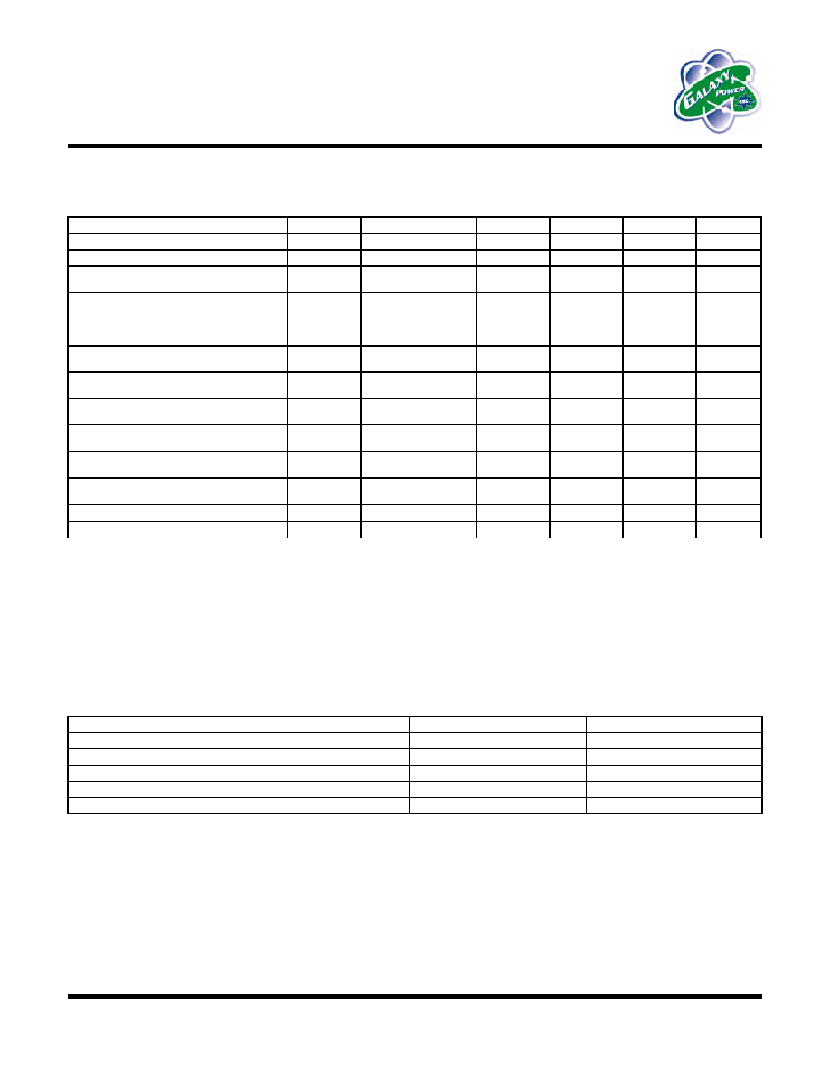
Table 5: Mode Select List
Table 4: Charge Rate List
SEL0
SEL1
Charge Rate
Topping Charge
pulse Rate
Maintenance Charge Pulse
Rate
Fast Charge Timer
Duration (after reset)
L
L
4C (15 min)
one every 40 sec
one every 160 sec
21 min
L
H
2C (30 min)
one every 20 sec
one every 80 sec
39 min
L
Z
1.3C (45 min)
one every 13 sec
one every 53 sec
57 min
H
L
1C (60 min)
one every 10 sec
one every 40 sec
75 min
H
Z
C/1.5 (90 min)
one every 7 sec
one every 27 sec
110 min
H
H
C/2 (120 min)
one every 5 sec
one every 20 sec
144 min
Z
L
C/2.5 (150 min)
one every 4 sec
one every 16 sec
212 min
Z
Z
C/3 (180 min)
one every 3 sec
one every 13 sec
244 min
Z
H
C/4 (240 min)
one every 2 sec
one every 10 sec
275 min
See the section on Controller Operation for additional information on the topping charge and maintenance charge. See the section on Charge Termination
Methods for additional information on the charge timer.
AUX0
AUX1
Mode Selected
Mode Operation
L
L
Charging System Test
Charging system test for embedded applications
L
H
Direct Maintenance
Indefinite C/40 maintenance charge
Z
Z
Fast Charge
Default
Z
L
Discharge-Only
Battery discharge to 1V/cell
H
L
Discharge-to-Charge
Battery discharge to 1V/cell followed by the selected charge mode
H
Z
Condition
Timed C/10 topping charge followed by a C/40 maintenance charge
H
H
Ten Hour Timer
Limits total charge including the maintenance charge to 10 hours

13
ICS1702
Master Reset: MRN Pin
The MRN pin is provided to re-program the controller for a new
mode or charging sequence. This pin has an internal pull-up of
about 75k
. A logic low on the MRN pin must be present for more
than 700ms for a reset to occur. As long as the pin is low, the
controller is held in a reset condition. A master reset is required to
clear a temperature fault condition, clear the charging system test,
reset the ten hour timer or change charge rates or auxiliary modes.
Upon power-up, the controller automatically resets itself.
Clock Input: RC Pin
The RC pin is used to set the frequency of the internal clock when
an external 1 MHz clock is not available. An external resistor must
be connected between this pin and V
DD
. An external capacitor
must be connected between this pin and ground. The frequency of
the internal clock will be about 1 MHz with a 16k
resistor and a
100pF capacitor. All time durations noted in this document are
based on a 1 MHz clock. Operating the clock at a lower frequency
will proportionally change all time durations. Operating the clock
at a frequency significantly lower than 1 MHz, without adjusting
the charge current accordingly, will lessen the effectiveness of the
fast charge timer and lower the accuracy of the controller.
Operating the clock at a frequency greater than 1 MHz will also
change all time durations and, without adjusting the charge current
accordingly, may cause termination to occur due to the fast charge
timer expiring rather than by the battery reaching full charge.
The clock may be driven by a 1 MHz external 0 to 5V pulse
provided the duty cycle is between 10% and 60%. The clock input
impedance is about 1k
.
Temperature Sensing: THERM Pin
The THERM pin is provided for hot and cold battery detection and
for temperature slope termination of fast charge when used in
conjunction with an NTC thermistor. The THERM pin also
provides for hot battery and maximum temperature termination
when used in conjunction with a normally closed thermal switch.
Several internal voltage thresholds are used by the controller
depending on whether a thermistor or a thermal switch is used.
Figure 9 shows the internal thresholds over laid on a typical
thermistor curve.
∑
Using an NTC thermistor for hot and cold battery
detection:
Figure 9:Voltage levels for temperature
sensing with a thermistor or thermal switch
The THERM pin requires some thought if a thermistor is going to
be used for hot and cold battery detection. The example below
works for a typical 10k
@ 25
∞
C NTC thermistor. Consider using
the controller to prevent charging above 45
∞
C and reducing the
current below 10
∞
C. At 10
∞
C the resistance of the thermistor is
18k
. At 45
∞
C, the resistance drops to 4.7k
. The ICS1702 has
an internal voltage threshold at 10
∞
C at 2.4V, and an internal
voltage at 45
∞
C at 0.93V as shown in Figure 9. At 25
∞
C the voltage
at the THERM pin is set at the midpoint of the thresholds:
0.93V + 2.40V - 0.93V =1.67V.
2
The THERM pin has a 75k
internal pull-up (R
pu
). Using a
resistor divider with 10k
for the thermistor (R
th
) and a external
fixed resistor (R
fix
), the divider looks like Figure 8 at 25
∞
C:
Figure 10: Voltage divider at the THERM pin
at 25
∞
C
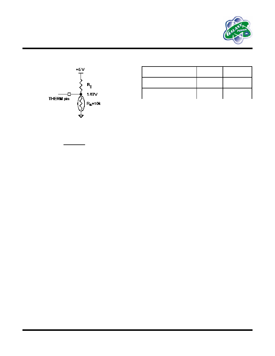
14
ICS1702
To set the voltage at the THERM pin for 1.67V at 25
∞
C, the
equivalent divider looks like Figure 11.
Table 6: Thermistor Voltage Thresholds
Figure 11: Equivalent voltage divider
The parallel resistance R
||
is calculated:
R
||
= 5V - 1.67V =20k
.
1.67V/10k
The internal pull-up resistance R
pu
and the parallel resistance R
||
are
known so the external fixed resistor can be calculated from:
R
pu
R
||
R
fix
= __________ .
R
pu
-
R
||
Substituting in known values: R
fix
= 27.27k
. A 27k
standard
value is used for R
fix
.
Since the thermistor resistance R
th
is specified by manufacturers at
a particular temperature, the voltage across the thermistor V
th
at
that temperature can be calculated from:
R
th
(5V)
V
th
= __________ (5V),
R
pu
+
R
||
with the drop across the resistor divider equal to 5V. For this
example, the calculated voltage with R
th
=18k
at 10
∞
C is 2.37V
and with R
th
=4.7k
at 45
∞
C the voltage is 0.95V. Table 6 lists the
internal thresholds for hot and cold battery detection. If the voltage
across the thermistor (at the THERM pin) drops below 0.93V, the
ICS1702 will shut down due to a hot battery fault condition and
will not restart unless reset. If the voltage dropped across the
thermistor is above 2.4V before fast charge is initiated, the
ICS1702 will begin a reduced current charge. See the Cold Battery
Charging section for more information.
∑
Using an NTC thermistor for temperature slope
termination:
As a battery approaches full charge, its accelerated rate of heating
can be used to terminate fast charge by detecting the large change
in the temperature slope. The large change in temperature slope is
proportional to the thermistor voltage change per unit of time. If
the DTSEL pin is programmed for temperature slope termination,
the controller will calculate the thermistor voltage slope and
terminate based on internally set thresholds as listed in Table 1.
The threshold is 40mV per minute for selected charge rates greater
than C/2, 28mV per minute for charge rates selected at or between
C/2 and C/3, and 18mV per minute for selected charge rates less
than C/3. The voltage across the thermistor must change at these
rates or greater to terminate the selected charge rate.
These thresholds correspond to a set change in thermistor
resistance when an external pull-up to 5V is used as shown in
Figure 11. Using the values calculated from the hot and cold
battery detection example, the percent change in the thermistor
resistance per minute for selected charge rates are provided. For
selected charge rates greater than C/2, the thermistor resistance
must decrease 4%/min. to terminate charge. For selected charge
rates at or between C/2 and C/3, the thermistor resistance must
decrease 3%/min. to terminate charge. For selected charge rates
less than C/3, the thermistor must decrease 2%/min. to terminate
charge.
Parameter
Voltage
Battery
Temperature
Cold Battery Thermistor
Voltage
>2.4
<10
∞
C
Hot Battery Thermistor
Voltage
<0.93
>45
∞
C

15
ICS1702
Figure 12: Thermal switch to connection to
ground at the THERM pin
Table 7: Thermal Switch Voltage Thresholds
The 4%/min., 3%/min. and 2%/min. decrease in thermistor
resistance for the last minute of charge for the selected charge rate
are applicable for NTC thermistors other than 10k
@ 25
∞
C
provided that the following requirements are met:
∑
An external pull-up resistor to 5V is used to provide a
∑
thermistor voltage of 1.67V @ 25
∞
C.
∑
The thermistor resistance at 25
∞
C does not exceed 20k
so
that accuracy and adequate noise immunity are maintained.
∑
The thermistor resistance increases by a factor of about 1.8
from 25
∞
C to 10
∞
C and the thermistor resistance decreases by
a factor of about 2.1 from 25
∞
C to 45
∞
C.
∑
Using a thermal switch for hot battery detection:
A thermal switch that opens at about 45
∞
C is recommended. The
thermal switch must be connected between the THERM pin and
ground. When the thermal switch is closed, the voltage at the
THERM pin must be below 0.5V for normal operation. When the
thermal switch opens (see Figure 12), the internal pull-up at the
THERM pin will raise the voltage above 4.2V and the ICS1702
will shut down and will not restart unless reset. Table 7 contains
the internal voltage thresholds used with a thermal switch.
For example, a battery was monitored as it charged at a 1C rate in
25
∞
C ambient. In the final minute of charge, the battery
temperature rose from 29.8
∞
C to 31
∞
C where full charge was
detected. With this data, the typical 10k
@ 25
∞
C thermistor used
in the example above is checked to determine if its characteristics
satisfy the 4% decrease in resistance required for the last minute of
charge. The thermistor measures 8.37k
@ 29.8
∞
C and 8.01k
at
31
∞
C. For a 1C charge rate, the resistance must decrease at least
4%/min. or more between 29.8
∞
C and 31
∞
C. The percent decrease
in resistance for the thermistor is calculated as:
8.37k
- 8.01k
(100) =4.30%
8.37k
This thermistor meets the 4%/min. requirement and will result in
termination at full charge at 31
∞
C. The thermistor must be checked
for a 4%/min. decrease in resistance for the last minute of charge
near the hot and cold battery thresholds.
The battery in the example above was charged in a 25
∞
C ambient
with its temperature rising 31
∞
C - 25
∞
C or 6
∞
C. The temperature
rise was 31
∞
C - 29.8
∞
C or 1.2
∞
C in the last minute before full
charge occurred. This information is used to check the thermistor
characteristics at the ambient extremes. If the selected 1C charge
rate is initiated at 12
∞
C, the thermistor resistance change must
decrease 4%/min. between 16.8
∞
C and 18
∞
C. The thermistor
resistance at 16.8
∞
C is 13.68k
and at 18
∞
C the thermistor
resistance is 13.06k
.
13.68k
- 13.06k
(100) =4.53%
13.68k
The thermistor meets the 4%/min. requirement and will result in
termination of fast charge at 18
∞
C. If the selected 1C charge rate is
initiated at 37
∞
C, the thermistor resistance change must decrease
4%/min. between 41.8
∞
C and 43
∞
C. The thermistor resistance at
41.8
∞
C is 5.48k
and at 43
∞
C the thermistor resistance is 5.25k
.
5.48k
-5.25k
(100) =4.19%
5.48k
The thermistor meets the 4%/min. requirement and will result in
termination of fast charge at 43
∞
C.
THERM pin
R = 75k
normally closed thermal switch
opens at 45∫C
V
DD
pu
Parameter
Voltage
Battery
Temperature
Open Thermal Switch
Voltage
>4.2
>45
∞
C
Closed Thermal Switch
Voltage
<0.5
<45
∞
C

16
ICS1702
Figure 13: Resistor divider network
at the VIN pin
Open Circuit Voltage Reference: OPREF Pin
The OPREF pin requires an external resistor divider to establish
the open circuit (no battery) voltage reference. The purpose of this
voltage reference is to detect the removal of the battery from the
charging system. The voltage at this pin is compared to the voltage
at the VIN pin when the current source is turned on. If the voltage
at VIN is greater than the voltage at OPREF, the ICS1702 assumes
the battery has been removed and the ICS1702 enters the polling
detect mode.
For proper operation, the voltage at OPREF must be set between
the (divided down) open circuit voltage produced by the current
source and the maximum normalized battery voltage. An example
is shown in Figure 14.
Suppose that a current source has an open circuit voltage of 12V.
The maximum expected battery voltage of a six-cell pack is
determined to be 9.6V. The voltage at OPREF should be set at a
point between 1.6V (9.6V/6 cells=1.6V) and 2V (12V/6=2V). This
is accomplished with a resistor divider network. In this example,
R4 and R3 are referred to V
DD
. Refer to the VIN and OPREF
divider resistor tables in the Applications Information section.
From the VIN table, the divider resistors are 10k
and 2k
for R1
and R2. From the OPREF table, the divider resistors are 2.2k
and
1.3k
for R3 and R4. If R3 is 2.2k
and R4 is 1.3k
, the voltage
at OPREF is 1.86V.
∑
Using no temperature sensor:
If a temperature sensor is not used, the THERM pin must be
grounded.
Termination Selection: DTSEL Pin
The ICS1702 has the capability of either temperature slope
termination, voltage slope termination or both methods
simultaneously. The DTSEL pin has an internal 75k
pull-down
resistor that enables voltage slope termination as the primary
method and is the default condition. Tying the pin high enables
both temperature slope and voltage slope termination methods.
Temperature slope termination as the primary method is enabled by
tying the DTSEL pin to the CMN output (pin 5). CMN must have
an external 15k
or lower value pull-up resistor to V
DD
for proper
activation of temperature slope termination. The ICS1702 must be
reset if a new termination method is desired. Table 8 summarizes
the DTSEL pin settings. NOTE: Maximum temperature and fast
charge timer termination methods are always enabled when using
temperature slope termination. Refer to the sections on Fast
Charge Timer Termination and Maximum Temperature
Termination for more information.
Table 8: Termination Select List
Voltage Input: VIN Pin
The battery voltage must be normalized by an external resistor
divider network to one cell. The electrochemical potential of one
cell is about 1.2V. For example, if the battery consists of six cells
in series, the voltage at the VIN pin must be equal to the total
battery voltage divided by six. This can be accomplished with two
resistors, as shown in Figure 13. To determine the correct resistor
values, count the number of cells to be charged in series. Then
choose either R1 or R2 and solve for the other resistor using:
R1 = R2 * (# of cells -1) or R2 = R1
(# of cells -1)
R1
R2
VIN pin
# of cells
Tie DTSEL
Pin to ...
Result
Low
(No Connect)
Voltage slope termination only
High
Voltage slope and temperature slope
termination
CMN
Temperature slope termination only
(CMN with external pull-up to V
DD
)
17
ICS1702
Data Tables
Table 9: Absolute Maximum Ratings
Power: VDD Pin
The power supply for the device must be connected to the VDD
pin. The voltage should be +5 VDC and should be supplied to the
part through a regulator that has good noise rejection and an
adequate current rating. The controller requires up to a maximum
of 11mA with V
DD
=5.00V.
Figure 14: Open Circuit Reference Example
Grounding: VSS, AVSS Pins
There are two ground pins. Both pins must be connected together
at the device. This point must have a direct connection to a solid
ground plane.
Supply Voltage
6.5
V
Logic Input Levels
-0.5 to V
DD
+ 0.5
V
Ambient Operating Temperature
0 to 70
∞
C
Storage Temperature
-55 to 150
∞
C
Stresses above those listed under Absolute Maximum Ratings may cause permanent damage to the device. This is a stress rating only.
Functional operation of the device at the Absolute Maximum Ratings or other conditions not consistent with the characteristics shown in this
document is not recommended. Exposure to absolute maximum rating conditions for extended periods may affect product reliability.
+ 5 V
R4 = 1.3k
R3 = 2.2k
R1 = 10k
R2 = 2k
6 cells
+
-
VIN =
OPREF = 1.86V
current source
(open circuit voltage = 12V)
{
1.60V (battery present)
2.00V (no battery)
(9.6 V)
Resistor divider at the OPREF pin
Resistor divider at the VIN pin
18
ICS1702
Table 10: DC Characteristics
Table 11: DC Voltage Thresholds
T
amb
=25
∞
C. All values given are typical at specified V
DD
.
Parameter
Symbol
Test Conditions
MIN
TYP
MAX
UNITS
Supply Voltage
V
DD
4.5
5.0
5.5
V
Supply Current
I
DD
7.3
mA
High Level Input Voltage
SEL0, SEL1, AUX0, AUX1
V
IH
3.6
4.1
4.5
V
Low Level Input Voltage
SEL0, SEL1, AUX0, AUX1
V
IL
0.73
0.75
0.8
V
Open Input Voltage
SEL0, SEL1, AUX0, AUX1
open
2.3
V
Low Level Input Current, pull-up
THERM, MRN
I
IL
V=0.4V
74
µ
A
High Level Input Current, pull-down
THERM, MRN
I
IH
V= V
DD
- 0.4V
75
µ
A
High Level Source Current
CHG, DCHG
I
OH
V= V
DD
- 0.4V
28
mA
Low Level Sink Current
CHG, DCHG
I
OL
V=0.4V
25
mA
Low Level Sink Current, indicator
PFN, CMN, MMN
I
OL
V=0.4V
40
mA
Low Level Sink Current, indicator
OTN
I
OL
V=0.4V
28
mA
Input Impedance
1.0
M
Analog/Digital Converter Range
0-2.2
0-2.7
0-2.7
V
T
AMB
=25
∞
C
PARAMETER
TYP
UNITS
Minimum Battery Voltage
0.5
V
Thermistor - Cold Temperature
2.4
V
Thermistor - Hot Temperature
0.93
V
Thermal Switch - Open
4.2
V
Thermal Switch - Closed
0.5
V

19
ICS1702
Table 12: Timing Characteristics
Timing Diagrams
Figure A:
Figure B:
t
CYCLE
t
DA
t
CHG
t
R
t
DA
CHG
DCHG
t
DCHG
t
R
t
R
voltage
temperature
R
16k
, C
100pF
PARAMETER
SYMBOL
REFERENCE
TYP
UNITS
Clock Frequency
1.0
MHz
Reset Pulse Duration
t
RESET
see Figure B
700
ms
Charge Pulse Width
t
CHG
see Figure A
1048
ms
Discharge Pulse Width
t
DCHG
see Figure A
5.0
ms
Rest Time
t
R
see Figure A
4.0
ms
Data Acquisition Time
t
DA
see Figure A
16.4
ms
Cycle Time
t
CYCLE
see Figure A
1077
ms
Capacitor Discharge Pulse Width
5.0
ms
Capacitor Discharge Pulse Period
100
ms
Polling Detect Pulse Width
100
ms
Polling Detect Pulse Period
624
ms
Soft Start Initial Pulse Width
200
ms
Soft Start Incremental Pulse Width
7.0
ms
Discharge Mode Pulse Width
400
ms
Discharge Mode Pulse Period
1050
ms
RESET to SEL Dynamic Reprogram Period
t
RSA
see Figure B
1160
ms
RESET to AUX Dynamic Reprogram Period
t
RSA
see Figure B
1160
ms
t
RSA
t
RESET
RESET
SEL0
SEL1
AUX0
AUX1

20
ICS1702
With the batteries removed, the current source must be capable of
raising the voltage at the VIN pin above the voltage at the OPREF
pin to ensure proper polling. With the batteries installed, the
current source overshoot characteristics when turned on and off
must not cause the voltage at the VIN pin to exceed the voltage at
the OPREF pin. If the voltage at OPREF exceeds the voltage at
VIN when a charge pulse is applied or removed, the polling feature
will be activated.
PC Board Design Considerations
It is very important that care be taken to minimize noise coupling
and ground bounce. In addition, wires and connectors can add
significant resistance and inductance to the charge and discharge
circuits. When designing the printed circuit board, make sure
ground and power traces are wide and bypass capacitors are used
right at the controller. Use separate grounds for the signal, charge
and discharge circuits. Separate ground planes on the component
side of the PC board are recommended. Be sure to connect these
grounds together at the negative lead of the battery only. For the
discharge circuit, keep the physical separation between power and
return (ground) to a minimum to minimize field radiation effects.
This precaution is also applicable to the constant current source,
particularly if it is a switch mode type. Keep the ICS1702 and the
constant current source control circuits outside the power and
return loop described above. These precautions will prevent high
circulating currents and coupled noise from disturbing normal
operation.
Selecting the Appropriate Termination Method
In general, the voltage slope termination method works best for
equipment where the battery is fast charged with the equipment off
or the battery is removed from the equipment for fast charge. The
temperature slope and maximum temperature termination methods
are for equipment that must remain operative while the battery is
fast charged.
Applications Information
To ensure proper operation of the ICS1702, external components
must be properly selected. The external current source used must
meet several important criteria to ensure optimal performance of
the charging system. The charging current should be constant when
using voltage slope termination. The current may vary when using
temperature slope termination.
VIN and OPREF Divider Resistors
Figure 15 shows a typical application using the ICS1702. R1
through R4 must be carefully selected to ensure that battery
detection and voltage termination methods operate properly.
R1 and R2 are selected to scale the battery voltage down to the
voltage of one cell. The following table shows some typical values.
Additional information is available in the Voltage Input section.
Cells
R1
R2
1
Short
Open
2
2.0k
2.0k
3
2.0k
1.0k
4
3.0k
1.0k
5
12k
3.0k
6
10k
2.0k
7
12k
2.0k
8
9.1k
1.3k
If using voltage slope termination, the current source should
prevent ripple voltage from appearing on the battery. The effects of
ripple on the battery voltage may interfere with proper operation
when using the voltage slope method.
R3 and R4 are used to set the open circuit (no battery) reference
voltage on the OPREF pin. The function of this pin is discussed in
the Open Circuit Reference section.
V
OPREF
R3
R4
1.86 V
2.2k
1.3k
1.92 V
2.4k
1.5k
1.97 V
2.0k
1.3k
2.00 V
3.0k
2.0k
2.03 V
2.2k
1.5k
2.10 V
1.8k
1.3k
2.14 V
2.4k
1.8k
2.22 V
3.0k
2.4k

21
ICS1702
∑
Temperature Slope and Maximum Temperature
Temperature slope and/or maximum temperature termination may
have to be used for equipment that has high dynamic current
demands while operating from the battery during fast charge. Also,
users who do not have a well regulated constant current source
available may have to use temperature termination. In general,
utilizing temperature slope as the primary termination method with
maximum temperature termination as a safety back-up feature is
the best approach. When using temperature slope termination, the
actual current should not be appreciably lower than the selected
rate in order that termination of fast charge occurs due to the
battery reaching full charge rather than by the timer expiring.
Temperature termination methods require that the thermal sensor
be in intimate contact with the battery. A low thermal impedance
contact area is required for accurate temperature sensing. The area
and quality of the contact surface between the sensor and the
battery directly affects the accuracy of temperature sensing.
Thermally conductive adhesives may have to be considered in
some applications to ensure good thermal transfer from the battery
case to the sensor.
The thermal sensor should be placed on the largest surface of the
battery for the best accuracy. The size of the battery is also a
consideration when using temperature termination. The larger the
battery the lower the surface area to volume ratio. Because of this,
larger batteries are less capable in dissipating internal heat.
Additional considerations beyond the basics mentioned above may
be involved when using temperature slope termination where
sudden changes in ambient temperature occur or where forced air
cooling is used. For these applications, the surface area of the
thermal sensor in contact with the battery compared to the surface
area of the thermal sensor in contact with the ambient air may be
significant. For example, bead type thermistors are relatively small
devices which have far less thermal capacity compared to most
batteries. Insulating the surface of the thermistor that is in contact
with the ambient air should help minimize heat loss by the
thermistor and maintain accuracy.
∑
Voltage Slope Termination
The voltage slope termination method used by the ICS1702
requires a nearly constant current flow into the battery during fast
charge. Equipment that draws a known constant current while the
battery is charging may use the voltage slope termination method.
This constant current draw must be added to the fast charge
current. Using the voltage slope termination method for equipment
that randomly or periodically requires moderate current from the
battery during fast charge needs evaluation. Equipment that
randomly or periodically requires high current from the battery
during fast charge may cause a voltage inflection that results in
termination before full charge. A voltage inflection can occur due
to the charge current decreasing or fluctuating as the load changes
rather than by the battery reaching full charge. The voltage slope
method will terminate charge based on voltage inflections that are
characteristic of a fully charged battery.
Charging sources that produce decreasing current as fast charge
progresses may also cause a voltage inflection that may result in
termination before full charge. For example, if the charge current is
supplied through a resistor or if the charging source is a constant
current type that has insufficient input voltage, the current will
decrease and may cause a termination before full charge. Other
current source abnormalities that may cause a voltage inflection
that is characteristic of a fully charged battery are inadequate ripple
and noise attentuation capability or charge current decreasing due
to thermal drift. Charging sources that have any of the above
characteristics need evaluation to access their suitability for the
application if the use of the voltage slope termination is desired.
When using voltage slope termination, the controller soft start
stage, built-in noise filtering, and fast charge timer operate
optimally when the constant current source charges the battery at
the rate selected. If the actual charge current is significantly less
than the rate selected, the conditioning effect of the soft start stage
and the controller noise immunity are lessened. Also, the fast
charge timer may cause termination based on time duration rather
than by the battery reaching full charge due to inadequate charge
current.

22
ICS1702
Charging System Status by Indicator
The Indicator Description List in Table 3 contains displays that are
caused by charging system abnormalities. When the CMN
indicator is flashing with no other indicator active, there is voltage
present at the battery terminals with the current source off and no
battery. Check the current source and ensure that it produces no
more than the equivalent of 350mV/cell when turned off with no
battery. If the VIN divider resistors were not properly selected, an
open circuit voltage that is actually less than the equivalent of
350mV/cell with the charger off and no battery will not divide
down this open circuit voltage properly and produce the CMN
flash indication. Check the VIN divider and ensure that it properly
normalizes the battery voltage to the electrochemical potential of
about 1.2V cell. If the CMN flash indication occurs with the
battery installed, then the constant current source is producing
more than the equivalent of 350mV/cell when off and there is an
open connection between the charger terminals and the battery.
Check wires, connections, battery terminals, and the battery itself
for an open circuit condition.
If the CMN and OTN indicators are active together, this is an
indication that the battery temperature has dropped to below 10
∞
C
after a fast charge was initiated with the battery temperature
normal. If this condition is observed and the battery temperature
did not drop after high charge was initiated, check the thermistor
circuit mechanically for poor contact and electrically for excessive
noise.
If the MMN and CMN indicators are alternately flashing, the likely
cause is no battery with the ICS1702 programmed in the
discharge-to-charge auxiliary mode. If the battery is present, check
wires, connectors, battery terminals, and the battery itself for an
open circuit condition.
If the MMN indicator is flashing with the OTN indicator active,
this is an indication that the battery is cold while in either the
discharge portion of the discharge-to-charge mode or the discharge
only mode. When in the discharge-to-charge mode, if the battery
does not warm-up into the normal temperature range after the
discharge is complete, the ICS1702 will enter the maintenance
charge stage. When the battery warms-up, the discharge-to-charge
mode will repeat.

23
ICS1702
Figure 15: Functional Diagram
+ 5 V
1
2
3
4
5
6
7
8
9
10
11
12
13
14
15
16
17
18
19
20
ICS1702
CHG
DCHG
PFN
MMN
CMN
OTN
SEL0
VSS
AVSS
SEL1
MRN
RC
DTSEL
AUX0
AUX1
THERM
OPREF
VIN
VDD
CONSTANT
CURRENT
SOURCE
V
in
+ 5 V (note 5)
4.7µF
.047µF
.047µF
10k
@ 25∞C
open
@ 45∞C
+ 5 V
+ 5 V
R1
R2
R3
R4
R5 (note 1)
27k (note 4)
+ 5 V
100pF
16k
Q1 (note 2)
1k
(note 3)
390
390
POLL
CHG
MAINT
TEMP
+ 5 V
Notes:
1) Value of R5 determined by discharge current and capacity of battery pack.
2) Discharge FET is logic-level compatible in this application.
3) DC return of discharge FET must be connected close to negative battery terminal.
4) Resistor is needed only if a thermistor is used. Value may change depending on thermistor.
5) Regulated supply
6) Power ground; others are signal ground. Connect signal ground to power ground
at negative battery terminal only.
(note 6)
temperature
sense
options
unused

24
ICS1702
ICS 1702 ST
Package Information
Ordering Information
ICS1702N, ICS1702M, ICS1702MT
Example:
Prefix: ICS = Intelligent Charging Solution standard device
Device type: Consists of 3 to 5 digits or numbers
Package type:
N=
DIP (Plastic)
M=
300 mil SOIC
MT= 300 mil SOIC Tape and Reel
0.016
0.050
0.008
0.094
0.033
0.504
0.041
0.041
0.402
0.296
0.008
All package dimensions are in inches.
0.296
0.039
0.016
QuickSaver
Æ
GPI
ICS1702M
20-Pin SOIC Package (300 mil)
0.018
0.050
0.250
1.025
0.130
0.018
0.100
0.050
0.029
0.130
0.310
0.250
0.350
0.010
GPI
ICS1702N
QuickSaver
Æ
All package dimensions are in inches.
20-Pin DIP Package (300 mil)

25
ICS1702
IMPORTANT NOTICE
Galaxy Power Incorporated makes no claim about the capability of any particular battery (NiCd or NiMH) to accept a fast charge. GPI
strongly recommends that the battery manufacturer be consulted before fast charging. GPI shall be held harmless for any misapplication of
this device such as: exceeding the rated specifications of the battery manufacturer; charging batteries other than nickel-cadmium or nickel-
metal hydride type; personal or product damage caused by the charging device, circuit, or system itself; unsafe use, application, and/or
manufacture of a charging system using this device.
GPI reserves the right to make changes in the device data identified in this publication without further notice. GPI advises its customers to
obtain the latest version of all device data to verify that any information being relied upon by the customer is current and accurate.
GPI does not assume any liability arising out of or associated with the application or use of any product or integrated circuit or component
described herein. GPI does not convey any license under its patent rights or the patent rights of others described herein. In the absence of a
written or prior stated agreement to the contrary, the terms and conditions stated on the back of the GPI order acknowledgment obtain.
GPI makes no warranty of any kind with regard to this material, including, but not limited to, the implied warranties of merchantability and
fitness for a particular purpose.
GPI products are not designed, intended, or authorized for use as components in systems intended for surgical implant into the body, or other
applications intended to support or sustain life, or for any nuclear facility application, or for any other application in which the failure of the
GPI product(s) could create a situation where personal injury or death may occur. GPI will not knowingly sell its products for use in such
applications, and the buyer shall indemnify and hold harmless GPI and its officers, employees, subsidiaries, affiliates, representatives and
distributors against all claims, costs, damages, expenses, tort and attorney fees arising out of directly or indirectly, any claim of personal
injury or death associated with such unintended or unauthorized use, even if such claim alleges that GPI was negligent regarding the design
or manufacture of the part.
COPYRIGHT © 1998 Galaxy Power Incorporated

26
ICS1702
NOTES

27
ICS1702
NOTES

28
ICS1702
GPI Sales Offices
Headquarters
Galaxy Power, Inc.
PO Box 890
2500 Eisenhower Avenue
Valley Forge, PA 19482-0890
Phone:
1-610-676-0188
FAX:
1-610-676-0189
Internet:
www.galaxypower.com
January 19, 1999
GPI Sales Representative