
April 27, 2006
© Kionix 2006 Rev 0.5
Page 1 of 3
Ultra-Small Package -- 5x5x1.2mm DFN
Precision Tri-axis Orthogonal Alignment
Multiplexed Analog Output
High Shock Survivability
Excellent Temperature Performance
Low Noise Density
Very Low Power Consumption
Selectable Power Reduction Modes
User Definable Bandwidth
Factory Programmable Offset
and Sensitivity
Self-test Function
"Kionix" is a registered trademark of Kionix, Inc. Products described herein are protected by patents issued or pending. Information provided in this document is believed to
be accurate and reliable but is not guaranteed. Kionix does not assume responsibility for its use or distribution. No license is granted by implication or otherwise under any
patent or other rights of Kionix. Kionix reserves the right to change product specifications or discontinue this product at any time without prior notice.
36 Thornwood Dr. - Ithaca, NY 14850 USA tel: 607-257-1080 - fax: 607-257-1146 - www.kionix.com - info@kionix.com
Drop Detection
Gesture Recognition
Inclination and Tilt Sensing
Image Stabilization
Sports Diagnostics
Vibration Analysis
Static or Dynamic Acceleration
Inertial Navigation and Ded(uctive) Reckoning
KXPA4 Series Data Sheet
Accelerometers and Inclinometers
Multiplexed Analog Output
KXPA4-1050
-- Tri-Axis XYZ, 2.8V
KXPA4-2050
-- Tri-Axis XYZ, 3.3V
P
recision in Motion
Cell Phones and Handheld PDAs
Gaming and Game Controllers
Universal Remote Controls
Theft and Accident Alarms
GPS Recognition Assist
Hard-drive Protection
Pedometers
Computer Peripherals
Cameras and Video Equipment
These high-performance silicon micromachined linear
accelerometers and inclinometers consists of a sensor
element and an ASIC packaged in a 5x5x1.2mm Dual
Flat No-lead (DFN). The sensor element is fabricated
from single-crystal silicon with proprietary Deep Reactive
Ion Etching (DRIE) processes, and is protected from the
environment by a hermetically-sealed silicon cap wafer at
the wafer level.
The
KXPA4
series is designed to provide a high signal-to-
noise ratio with excellent performance over temperature.
These sensors can accept supply voltages between 2.7V
and 5.25V. Sensitivity is factory programmable allowing
customization for applications requiring ±1.5g to ±6.0g
ranges. Sensor bandwidth is user-definable.
The sensor element functions on the principle of
differential capacitance. Acceleration causes displace-
ment of a silicon structure resulting in a change in ca-
pacitance. An ASIC, using a standard CMOS manufactur-
ing process, detects and transforms changes in capaci-
tance into an analog output voltage, which is proportional
to acceleration. The analog output is also accessed
through an on-board 3 channel multiplexor. The sense
element design utilizes common mode cancellation to
decrease errors from process variation and
environmental stress.
APPLICATIONS
FEATURES
PROPRIETARY TECHNOLOGY

April 27, 2006
© Kionix 2006 Rev 0.5
Page 2 of 3
KXPA4 Series Data Sheet
PARAMETERS
UNITS KXPA4≠1050 KXPA4≠2050
CONDITION
Range
2
g
±2.0
Factory programmable
Sensitivity
mV/g
560
660
0g Offset vs. Temp.
mg
±150 (x and y) ±300 (z)
Over temp range
∞C
-40 to 85
3
Sensitivity vs. Temp
%
±2.0 max
Over temp range
Span
mV
±1120
±1320
Noise
175 typical
Bandwidth
4
Hz
0 to 3300 max (x and y)
-3dB
0 to 1700 max (z)
Output Resistance
5
32K typical
Non-Linearity
% of FS
0.1 typical (0.5 max)
Ratiometric Error
%
±0.4 typical (±1.5 max)
Cross-axis Sensitivity
%
±2.0 typical (±3.0 max)
Power Supply
V
2.8
1
3.3
1
V
-0.3 (min) 7.0 (max)
Absolute min/max
mA
1.1 typical
µA
<10
Shutdown pin connected to GND
ms
1.6
Power-up time @ 500 Hz
6
ENVIRONMENTAL SPECIFICATIONS
PARAMETERS
UNITS
KXPA4 Series
CONDITION
Operating Temperature
∞C
-40 to 85
7
Powered
Storage Temperature
∞C
-55 to 150
Unpowered
Mechanical Shock
g
4600
Powered or unpowered,
0.5 msec halversine
ESD
V
3000
Human body model
PERFORMANCE SPECIFICATIONS
1
PRODUCT SPECIFICATIONS
Notes
1
The performance parameters are programmed and tested at 2.8 volts (KXPA4-1050) and 3.3V (KXPA4-2050). However, the
device can be factory programmed to accept supply voltages from 2.7 V to 5.25 V. Operation at reduced supply voltages,
down to 2.6 V, can be achieved by narrowing the operating temperature range. Performance parameters will change with
supply voltage variations.
2
Custom ranges from 1.5g to 6g available.
3
Temperature range for specified offset.
4
Lower bandwidth can be achieved by using the external C
2
, C
3
, and C
4
(see application note on page 3).
5
32K
resistor connects the output amplifier to the output pin. Resistive loading may reduce sensitivity or cause a shift in
offset. Maintaining a load resistance at 3.2M
will prevent appreciable changes.
6
The power-up time will increase or decrease according to bandwidth (5RC).
7
0g offset and sensitivity change linearly with temperature.
CAUTION:
ELECTROSTATIC
SENSITIVE COMPO-
NENT
Hz
g /
µ
April 27, 2006
© Kionix 2006 Rev 0.5
Page 3 of 3
CAUTION:
ELECTROSTATIC
SENSITIVE COMPO-
NENT
KXPA4 Series Data Sheet
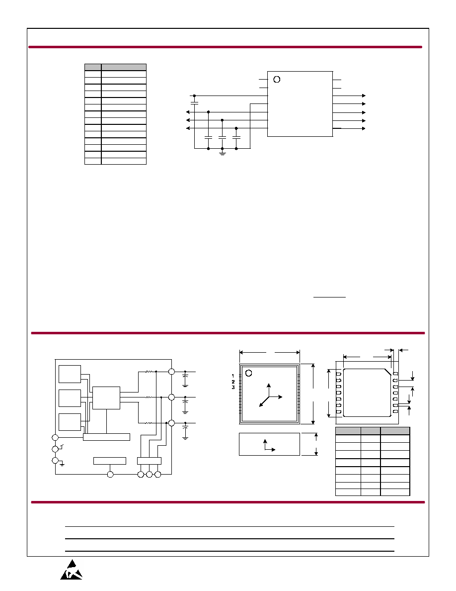
APPLICATION SCHEMATIC & PIN FUNCTION TABLES
KXPA4 Pin Descriptions
GND ≠ Ground
PS -- Power shutdown pin. When the PS pin is connected to GND or left floating, the KXPA4 is shutdown and drawing very little
power. When the PS pin is tied to Vdd, the unit is fully functional.
Self Test -- The output of a properly functioning part will increase when Vdd is applied to the self-test pin. When NOT in use,
this pin must be tied to ground.
SO -- MUX select
S1 -- MUX select
Vdd ≠ Power supply
Vmux -- Multiplexed analog output
Application Design Equations
The bandwidth is determined by the filter capacitors connected from pins 3, 4 and 5 to ground. The response is single pole.
Given a desired bandwidth, f
BW
, the filter capacitors are determined by:
Notes
1. Recommend using 0.1 µF for decoupling capacitor C
1
.
BW
f
x
C
C
C
6
4
3
2
10
97
.
4
-
=
=
=
Dimension Inches Millimeters
A
.197
5.00
B
.197
5.00
C
.047
1.20
D
.009
0.23
E
.020
0.50
F
.016
0.40
G
.142
3.60
H
.142
3.60
+Y
+X
+Z
+Z
+X
A
B
C
D
E
F
G
H
FUNCTIONAL DIAGRAM
5x5x1.2mm DFN PACKAGE
Product
Axis(es) of
Sensitivity
Range
Sensitivity
(mV/g)
Offset (V)
Operating
Voltage (V)
Temperature
Package
KXPA4-1050
XYZ
2g
560
1.40
2.8
-40 to +85 ∞C
5x5x1.2mm DFN
KXPA4-2050
XYZ
2g
660
1.65
3.3
-40 to +85 ∞C
5x5x1.2mm DFN
Pin
Tri-Axis Function
1
DNC
2
DNC
3
Vdd
4
GND
5
X Output
6
Z Output
7
Y Output
8
PS
9
Self Test
10
S1
11
S0
12
Vmux
13
DNC
14
DNC
X Output ≠ Analog X output
Y Output ≠ Analog Y output
Z Output ≠ Analog Z output
C
2
C
3
32K
X
Sensor
Oscillator
9
5
Self
Test
Output X
PS
Vdd
GND
4
3
Z
Sensor
Charge
Amplifier
32K
Output Z
6
Y
Sensor
32K
Output Y
7
8
Logic
C
4
MUX
11
10
12
S0 S1Vmux
ORDERING GUIDE
14
13
12
11
10
9
8
1
2
3
4
5
6
7
KXPA4
Vmux
S0
S1
ST
PS
C
2
C
3
C
1
C
4
Vdd
Notes:
1. When device is accelerated in +X, +Y or +Z
direction, the corresponding output will increase.
2. The packaged device weighs .079 grams.