1
5A Adjustable Low Dropout
Linear Regulator (LDO)
NIKO-SEM
L1084S5
TO-263
Rev. 1.0 MAR
GENERAL DESCRIPTION
The L1084 is a positive and low dropout
three-terminal voltage regulator with 5A out-
put current capability. This device is design-
ed for use in low voltage applications that
offers lower dropout voltage and faster tran-
sient response.
This device is fully protected against over
current faults, over temperature operation,
reversed input polarity, reversed lead insert-
ion, transient voltage spike ...etc.
On-Chips trimming the reference voltage to
1% and features the low dropout of maxi-
mum 1.45 volts.
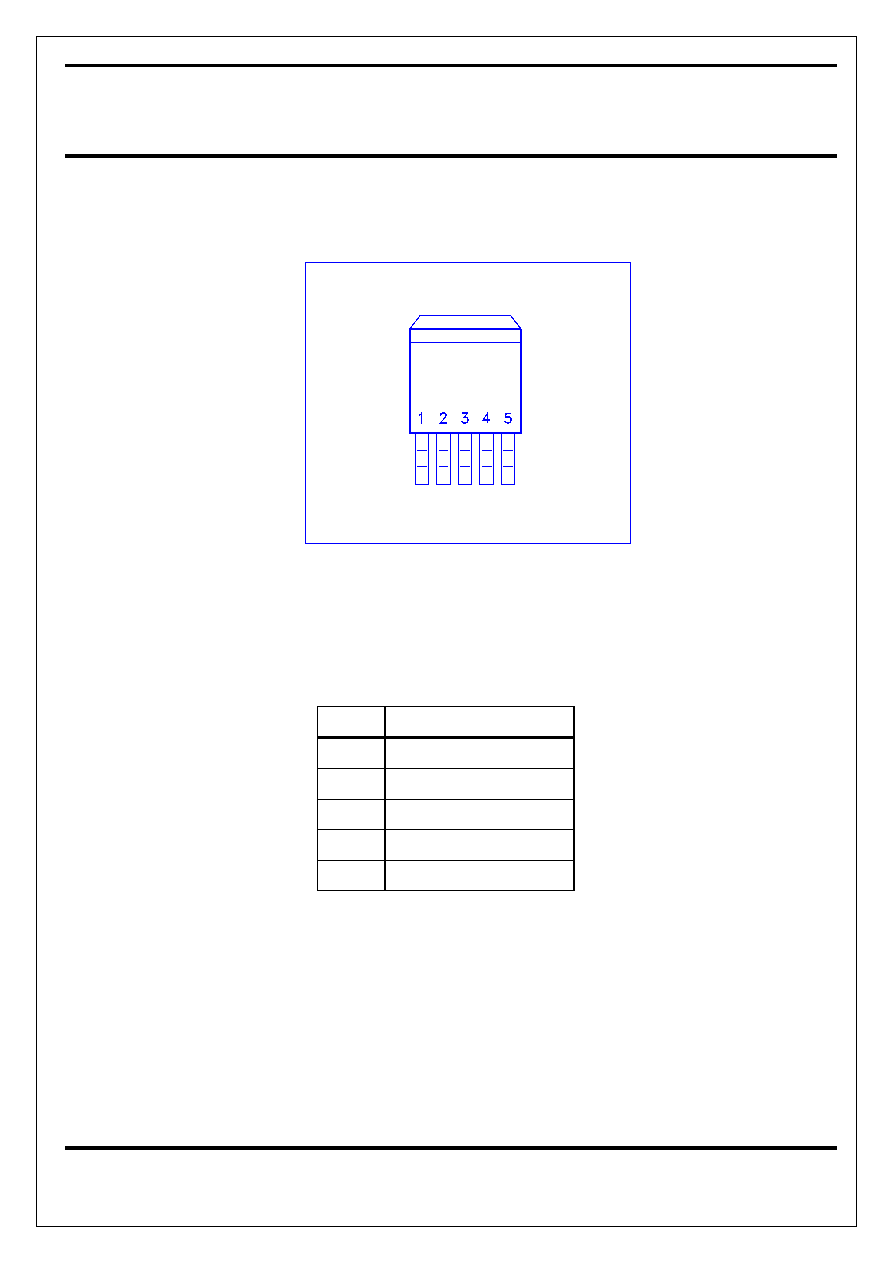
The L1084 Series regulators are available
in the popular industry standard TO-263
packages.
FEATURES
Very easy to use, it requires only two
external resistors to set the output voltage
Low dropout voltage:
1.2V typical at up to 5A
Low ground current
Fast transient response
Current & thermal limiting
Line regulation: 0.5% typical
Load regulation: 0.5% typical
TO-263 packages
APPLICATIONS
High current microprocessor supplies
Low voltage logic supply
Powering VGA & sound card
Portable instrumentation
Constant current regulator
Post regulator for switching power supply
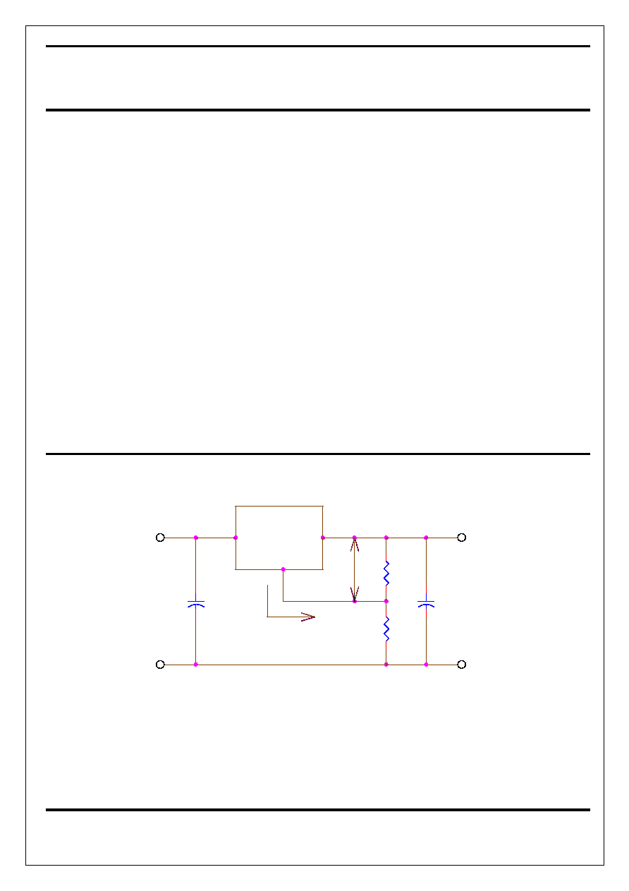
TYPICAL APPLICATION
- Basic Adjustable Regulator Circuit -
Vin
+
Cin
10uF
Vref
OUT
IN
Vo = Vref (1+R2/R1) + Iadj x R2
1. Cin needed if device is far from filter capacitors.
Vout
ADJ
R1
Iadj
L1084X5
5
3
2
+
Cout
10uF
2. Cout required for stability.
R2
2
5A Adjustable Low Dropout
Linear Regulator (LDO)
NIKO-SEM
L1084S5
TO-263
Rev. 1.0 MAR
ABSOLUTE MAXIMUM RATINGS
Maximum Supply Voltage
7V
Operating Junction
Temperature Range
0 to 125 �C
Power Dissipation
Internally
Limited
Storage Temperature
Range
-40 to 150 �C
Thermal Resistance
Junction to Case,
JC
2.5 �C/W
Lead Temperature
(Soldering, 10 Seconds)
260 �C
Thermal Resistance
Junction to Ambient,
JA
TO-263
60 �C/W
ELECTRICAL CHARACTERISTICS (
Unless otherwise specified, T
A
= 25 �C.)
Parameter
Symbol
Test Conditions
Typical
Limits
Reference Voltage
V
REF
V
IN
= 5V, I
OUT
= 10mA
1.25V
1.23V
Min
1.27V
Max
Dropout Voltage
V
D
V
REF
= 1%, I
OUT
= 5A
1.2V 1.45V
Line Regulation
REG
(LINE)
(V
OUT
+ 1.5V)
V
IN
7V, I
OUT
= 10mA
0.5% 2%
Load Regulation
REG
(LOAD)
(V
IN
-V
OUT
) = 3V, 10mA
I
OUT
5A
0.5% 2.5%
Minimum Load
Current
I
O
1.5V
(V
IN
-V
OUT
)
5.75V
10mA
Adjust Pin Current
I
ADJ
55
�
A 100
�
A
Current Limit
I
CL
V
IN
- V
OUT
= 2V
7.5A
5.0A (Min)
RMS Output Noise
V
N
0.003%
of V
OUT
Ripple Rejection
Ratio
R
A
f = 120Hz, C
ADJ
= 22
�
F for ADJ pin,
V
IN
= 5V, I
OUT
= 5A
72dB 60dB
(Min)
DEVICE SELECTION GUIDE
Device
L1084S5
Package
TO-263 (5-Lead)
Marking
L1084S5
4
5A Adjustable Low Dropout
Linear Regulator (LDO)
NIKO-SEM
L1084S5
TO-263
Rev. 1.0 MAR
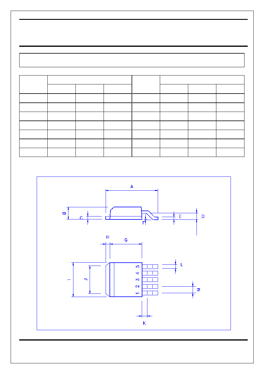
TO-263 (D
2
PAK, 5-Lead) MECHANICAL DATA
mm
mm
Dimension
Min. Typ. Max.
Dimension
Min. Typ. Max.
A 14.5 15 15.8 H 1.0 1.5 1.8
B 4.2 4.7 I 9.8 10.3
C 1.20 1.35 J 6.5
D 2.8 K 1.5
E 0.3 0.4 0.5 L 0.7 0.85 1.0
F -0.102 0.203 M 1.57 1.7 1.83
G 8.5 9 9.5 N