1
2.5V Low-Voltage Adjustable
Precision Shunt Regulator
NIKO-SEM
L431
JAN-08-Y02
GENERAL DESCRIPTION
The L431 is a three-terminal adjustable shunt
regulator utilizing an accurate 2.5V band-gap
reference. The output voltage can be set to any
value between 2.5V (V
REF
) to 29V with two
external resistors as shown in the typical
application circuit. The device exhibit a wide
operating current range of 0.4 to 100 mA with a
typical dynamic impedance of 0.25. The cha-
racteristics of these reference make it exce-
llent replacements for zener diodes in many
applications such as digital voltmeters, power
supplies, and op amp circuitry. The 2.5V volt
reference makes it convenient to obtain a
stable reference from 5.0V logic supplies.
The L431 shunt regulator is available in three
voltage tolerances (0.5%, 1.0% and 2%) and
three package options (TO-92, SOT-23-3,
SOT-23-5 and SOIC-8).
FEATURES
Internal amplifier with 70 mA capability
Programmable output voltage to 29V
0.25typical output impedance
Pin to pin compatible with TL431, LM431
, SC431 & AS431
Trimmed band-gap design 0.5%, 1.0%
and 2% with three package options
Low cost solution
APPLICATIONS
Linear regulator controller
Precision voltage reference
Switching power supplies
Battery operating equipment
Instrumentation
PCs, Computer disk drives
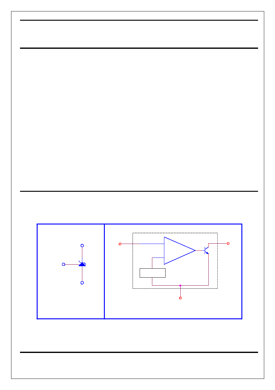
SYMBOL & BLOCK DIAGRAM
Anode (A)
Cathod
Reference
-
+
Cathode (K)
Anode (A)
Reference (R)
2.5 Vref
FUNCTIONAL BLOCK DIAGRAM
SYMBOL
(R)
(K)
2
2.5V Low-Voltage Adjustable
Precision Shunt Regulator
NIKO-SEM
L431
JAN-08-Y02
ABSOLUTE MAXIMUM RATINGS
PARAMETER
VALUE
Cathode-Anode Reverse Breakdown Voltage - V
KA
30V
Anode-Cathode Forward Current - I
AK
70
mA
Reference Input Current - I
REF
10
mA
Storage Temperature Range - T
STG
-65 to +150 �C
Junction Temperature - T
J
150
�C
Lead Temperature (Soldering, 10 Seconds) - T
L
300
�C
Continuous Power at 25 �C - P
D
TO-92
SOIC-8
SOT-23
700 mW
650 mW
200 mW
RECOMMENDED CONDITIONS
TYPICAL THERMAL RESISTANCES
Parameter
Rating
Package
JA
JC
Typ. Derating
Cathode Voltage (V
KA
) V
REF
to 29V
TO-92
160 �C/W
80 �C/W
6.3 mW/�C
Cathode Current (I
K
)
10 mA
SOIC-8
175 �C/W
45 �C/W
5.7 mW/�C
SOT-23 575 �C/W 150 �C/W
1.7 mW/�C
ELECTRICAL SPECIFICATIONS
(Ambient temperature must be derated base on power dissipation and package thermal characteristics. The conditions are: V
KA
= V
REF
and
I
K
= 10 mA unless otherwise stated)
PARAMETER
TEST CONDITIONS
MIN TYP MAX
UNITS
TEST
CIRCUIT
T
A
= 25 �C, L431 (0.5%) 2.482 2.495 2.507
T
A
= 25 �C, L431 (1%)
2.470 2.495 2.520
Reference Voltage
T
A
= 25 �C, L431 (2%)
2.445 2.495 2.550
V
1
V
REF
with Temp.
0.07
0.2
mV/�C
1
V
REF
to 10V
-2.7
-1.0
Ration of Change in V
REF
to
Cathode Voltage
10V to 30V
-2.0
-0.4
0.3
mV/V
2
Reference Input Current
0.7
4
�A
2
I
REF
Temp. Deviation
Over Temp.
0.4
1.2
�A
2
Min. I
K
for Regulation
0.4
1
mA
1
Off State Leakage
V
REF
= 0V, V
KA
= 30V
0.04
250
nA
3
Dynamic Output Impedance
f 1KHz, I
K
= 1 to 70 mA
0.25
0.5
1
3
2.5V Low-Voltage Adjustable
Precision Shunt Regulator
NIKO-SEM
L431
JAN-08-Y02
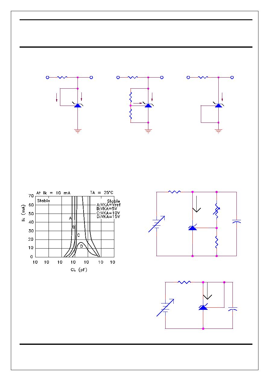
TEST CIRCUITS
IN
V
V
KA
K
I
REF
I
V
REF
R1
R2
- TEST CIRCUIT 2 -
>
(V
KA
V
REF
)
REF
I
)
V
KA
V
=
- TEST CIRCUIT 1 -
KA
V
REF
(V
IN
- TEST CIRCUIT 3 -
KA
V
V
IN
K (OFF)
I
(OFF STATE CURRENT)
I
K
The areas under the curves represent conditions that may
cause the device to oscillate. For curves B, C and D, R
1
and
V
BATT
were adjusted to establish the initial V
KA
and I
KA
conditions with C
L
= 0. V
BATT
and C
L
then were adjusted
to determine the ranges of stability.
Stability Boundary Condition For Shunt Regulation
VS. Cathode Current and Load Capacitance
1
0
2
3
4
5
6
CL
Ik
150
1
2
L431
2
3
1
Test Circuit for Vka = Vref
150
L431
2
3
1
10K
R2
Test Circuit for Vka > Vref
Ik
R1
CL
VBATT
1
2
4
2.5V Low-Voltage Adjustable
Precision Shunt Regulator
NIKO-SEM
L431
JAN-08-Y02
Small-Signal Gain and Phase Shift
VS. Frequency
VS. Cathode Voltage
Cathode Current
Cathode Current
VS. Cathode Voltage
VS. Junction Temperature
r
z
(
)
Reference Impedance
VS. Junction Temperature
Ratio of Delta Reference Voltage to Delta Cathode Voltage
V
r
e
f
/
V
z
(
-
m
V
/
V
)
Vz = 3V to 30V
8.25K
OUT
Ik
GND
15K
1
2
L431
2
3
1
10uF
232
1
2
Test Circuit for Small Signal Gain and Phase
5
2.5V Low-Voltage Adjustable
Precision Shunt Regulator
NIKO-SEM
L431
JAN-08-Y02
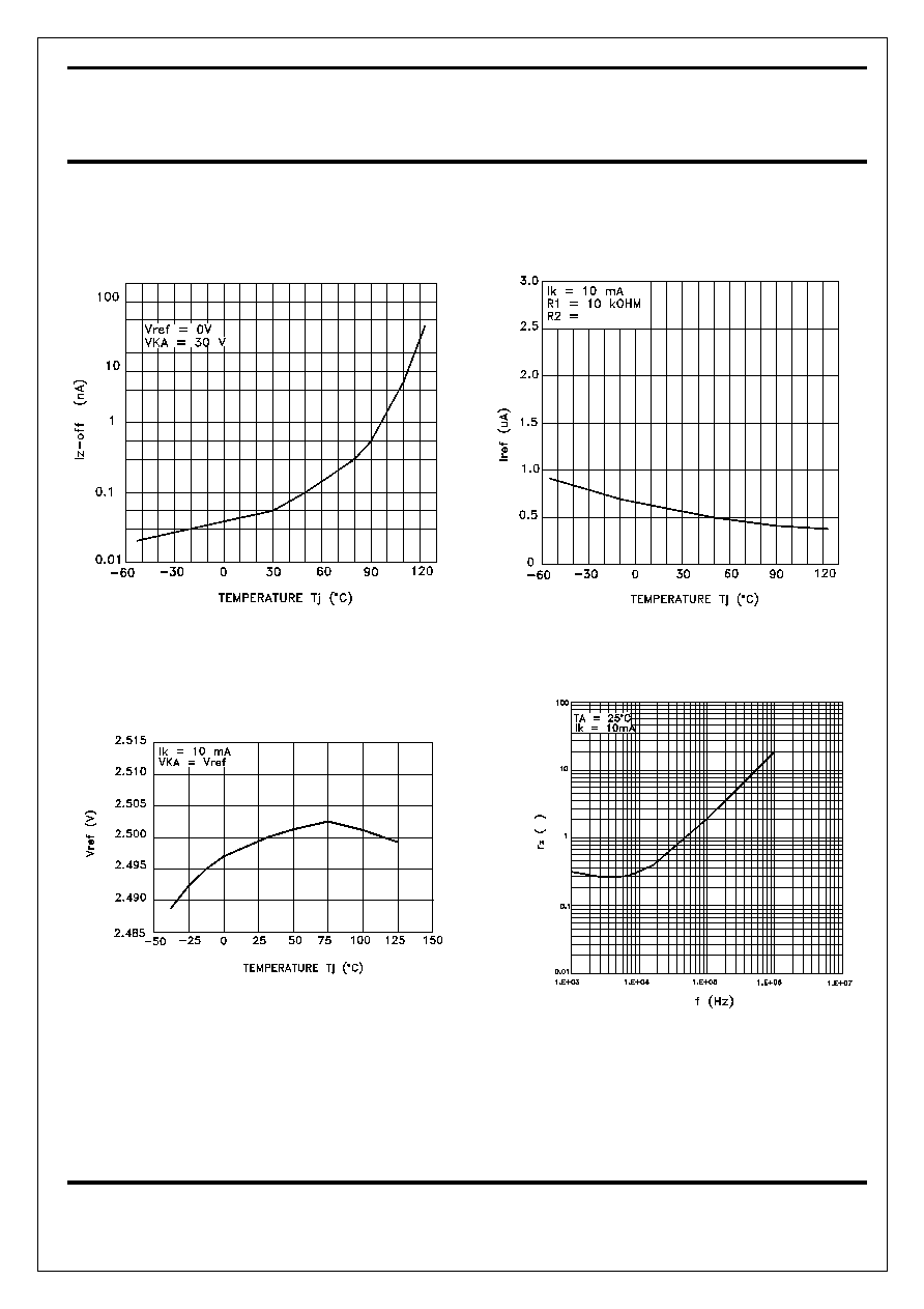
VS. Junction Temperature
Off-State Cathode Current
VS. Junction Temperature
Reference Voltage
VS. Frequency
Reference Impedance
Reference Input Current
VS. Junction Temperature