- 1 - Letex Technology Corp.
Photocoupler
Part Name: LA314
Features
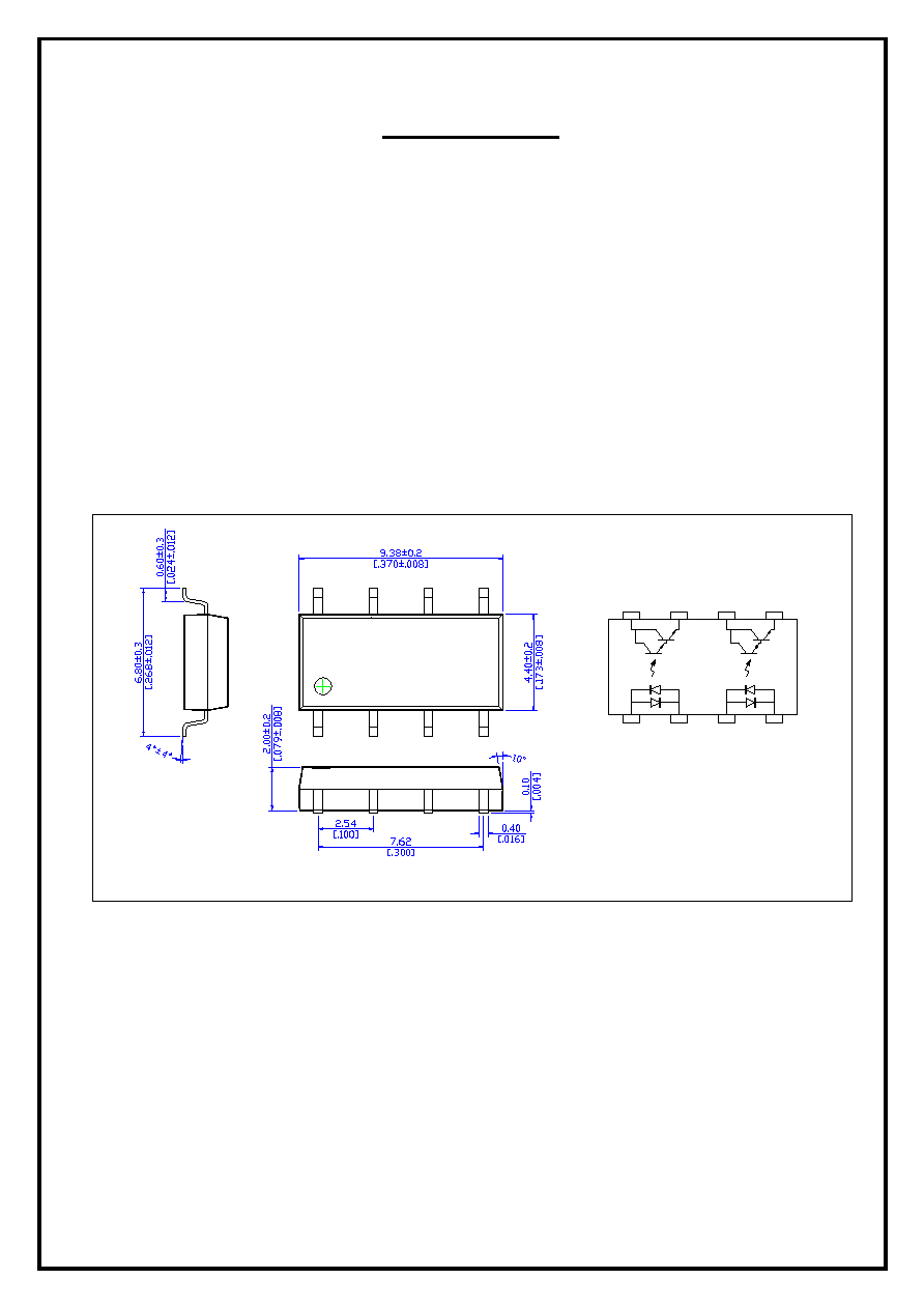
SOP package 4 Pin type in miniature design
600% minimum current transfer ratio
1500V rms Input/Output isolation
AC input.
Applications
Telephones
Programmable controllers
System appliances, measuring instruments.
Signal transmission between circuits of different potentials and impedances.
1,3. Anode,Cathode
2,4. Cathode, Anode
5,7. Emitter
6,8. Collector
General Tolerance:
�
0.1
Terminal Thickness: 0.15 [.006]
1
2
4
3
LA314
16A
Letex
1
2
3
4
Dimensions
(Unit: mm [inch])
8
7
6
5
8
7
6
5
- 2 - Letex Technology Corp.
Photocoupler
Part Name: LA314
Absolute Maximum Ratings
(Ambient Temperature: 25)
Item
Symbol
Rating
Units
Note
Forward Current
I
F
50
mA
Reverse Voltage
V
R
5
V
Input
Peak Forward Current
I
FP
1
A
Collector to Emitter Voltage
Vceo
40
V
Ic=1mA, I
B
=0
Emitter to Collector Voltage
Veco
6
V
I
E
=100�A, I
B
=0
Collector Current
Ic
50
mA
Output
Power Dissipation
Pc
150
mW
I/O Breakdown Voltage
V
I/O
1500
Vrms
RH=60%, 1min
Power Dissipation
P
D
200
mW
Storage Temperature
Tstg
-55 to +125
Operating Temperature
Top
-55 to +100
Soldering Temperature
T
Sol
260
10 seconds max.
Electrical Specifications
(Ambient Temperature: 25)
Item
Symbol
MIN.
TYP.
MAX.
Units
Conditions
Forward Voltage
V
F
1.2
1.4
V
I
F
=
�
20mA
Reverse Current
I
R
-
�A
Input
Junction Capacitance
Ct
30
pF
V=0, f=1.0KHz
C-E Breakdown Voltage
Vceo
35
V
Ic=0.5mA
E-C Breakdown Voltage
Veco
6
V
Ie=0.1mA
Output
Collector Dark Current
Iceo
100
nA
Vce=20V, I
F
=0
Current Transfer Ratio
CTR
600
1600
7000
I
F
=
�
1mA, Vce=5V
Collector Saturation Voltage
Vce(sat)
1
V
I
F
=
�
20mA, Ic=1mA
Isolation Resistance
R
I/O
10
9
V=500V DC
Isolation Capacitance
C
I/O
1.0
pF
V=0, f=1.0MHz
Rise Time
t
r
300
�s
Vce=5V, Ic=2mA,
Coupled
Fall Time
t
f
250
�s
RL=100
- 3 - Letex Technology Corp.
Photocoupler
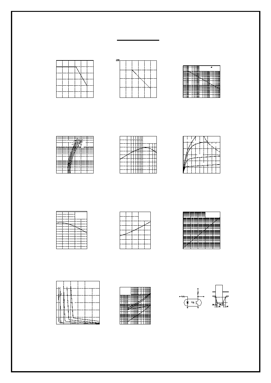
Reference Data
10
0.2
0
0
C
o
l
l
e
c
to
r
-
E
m
i
tt
e
r
s
a
tu
r
e
a
ti
o
n
vo
l
ta
g
e
(
V
)
0.4
0.6
0.8
Forward current (mA)
20
30
40
50
60
Collector-Emitter saturation voltage Vs.
Forward current
1.0
1.2
Test circuit for resopnse time
F
o
r
w
a
r
d
c
u
r
r
e
n
t
(
m
A
)
Forward voltage (V)
-25
0
Forward current Vs.
Forward voltage
Ambient temperature (
)
75
50
-25
0
Ambient temperature (
)
75
50
100
Forward current Vs.
Ambient temperature
F
o
r
w
a
r
d
c
u
r
r
e
n
t
(
m
A
)
10
20
30
40
50
60
Collector power dissipation Vs.
Ambient temperature
150
C
o
l
l
e
c
t
o
r
p
o
w
e
r
d
i
s
s
i
p
a
t
i
o
n
(
m
W
)
50
100
0
25
100
125
0
25
125
Peak forward current Vs.
Duty ratio
Duty ratio
P
e
a
k
f
o
r
w
a
r
d
c
u
r
r
e
n
t
(
mA
)
10
20
50
100
200
500
1000
2000
5 10 2
5
5
2
5
2
-3
-2
10
-1
10
0
10
3.0
2.5
1.0
0.5
1.5
2.0
1
10
50
200
0
Pulse width 100us
Ta = 25
2
5
100
500
20
25
0
25
50
Ta = 75
C
T
R
(
%
)
Forward current (mA)
1
1
Current transfer ratio Vs.
Forward current
2
5
10
20
50
20
40
60
80
100
120
140
160
180
200
Vce = 5V
Ta = 25
0
0
C
o
l
l
e
c
to
r
c
u
r
r
e
n
t
(
m
A
)
Collector-Emitter voltage (V)
Collector current Vs.
Collector-Emitter voltage
Ta = 25
1
2
3
4
5
6
7
8
9
5
10
15
20
25
30
I
F
= 30mA
20mA
10mA
5mA
Pc(Max)
R
e
l
a
ti
v
e
C
T
R
(
%
)
Ambient temperature (
)
-25
0
0
25
100
50
75
Relative CTR Vs.
Ambient temperature
50
100
150
I
F
= 5mA
Vce = 5V
C
o
l
l
e
c
t
o
r
-
E
m
i
t
t
e
r
s
a
t
u
r
a
t
i
o
n
v
o
l
t
a
g
e
(
V
)
Ambient temperature (
)
-25
0
0
25
100
50
75
Collector-Emitter saturation voltage Vs.
Ambient temperature
I
F
= 20mA
Ic = 1mA
0.02
0.04
0.06
0.08
0.10
0.12
0.14
0.16
Vce = 20V
Collector dark current Vs.
Ambient temperature
C
o
l
l
e
c
to
r
d
a
r
k
c
u
r
r
e
n
t
(
A
)
Ambient temperature (
)
-11
10
-10
10
-9
10
-8
10
-7
10
-6
10
-5
10
0
25
50
75
100
-25
7m
A
5m
A
3m
A
1m
A
I
c=
0
.
5
m
A
Ta = 25
R
e
s
p
o
n
s
e
t
i
m
e
(
s
)
Load resistance (k
)
0.1
Response time Vs.
Load resistance
Vce = 2V
Ic = 2mA
Ta = 25
0.1 0.2 0.5 1 2
5
10
0.2
0.5
1
2
5
10
20
50
100
200
500
Vcc
R
L
Output
R
D
Input
10%
Input
Output
90%