--
1--
Letex Technology Corp.
Subminiature Photointerrupter
Model No: LBT-125
Features
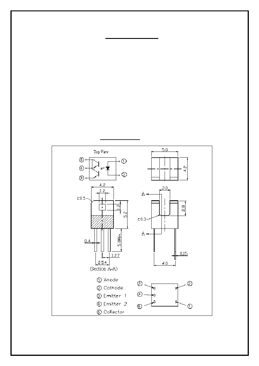
Compact package based on the double-mold method.
High resolution (slit width = 1.2mm).
Gap between emitter and detector is 2.0mm.
Applications
Floppy disk drives
Printers
Cameras
Outline Dimensions (Unit: mm)
--
2--
Letex Technology Corp.
Subminiature Photointerrupter
Model No: LBT-125
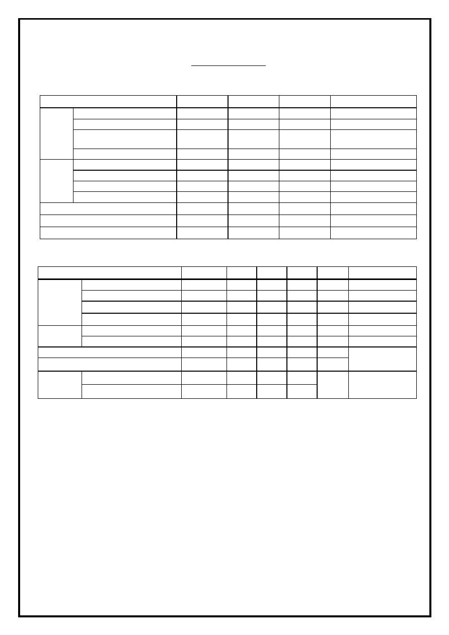
Absolute Maximum Ratings
(Ambient Temperature: 25)
Item
Symbol
Rating
Units
Note
Forward current
I
F
50
mA
Reverse voltage
V
R
5
V
Peak forward current
I
FP
1
A
Tw=10s,
t=10ms
Input
Power dissipation
Pd
75
mW
Collector current
Ic
50
mA
Collector-Emitter voltage
Vceo
30
V
Emitter-Collector voltage
Veco
5
V
Output
Collector power dissipation
P
c
100
mW
Storage Temperature
Tstg
-40 to +85
Operating Temperature
Top
-25 to +85
Soldering Temperature
Tsol
260
5 seconds max.
Electrical Specifications
(Ambient Temperature: 25)
Item
Symbol
MIN.
TYP.
MAX.
Units
Conditions
Forward voltage
V
F
1.2
1.4
V
IF=20mA
Reverse current
I
R
10
�A
VR=5V
Peak wavelength
p
940
nm
Input
View angle
21/2
35
Deg.
IF=20mA
Dark current
Iceo
100
nA
Vce=20V
Output
C-E saturation voltage
Vce(sat)
0.4
V
Ic=2mA, IB=0.1mA
Light current
Ic(on)
0.5
mA
Leakage current
I
Leak
1
�A
Vce=5V
IF=20mA
Rise Time
t
r
5
Speed
Fall Time
t
f
5
�s
Vce=5V
Ic=1mA
RL=1K
--
3--
Letex Technology Corp.
Subminiature Photointerrupter
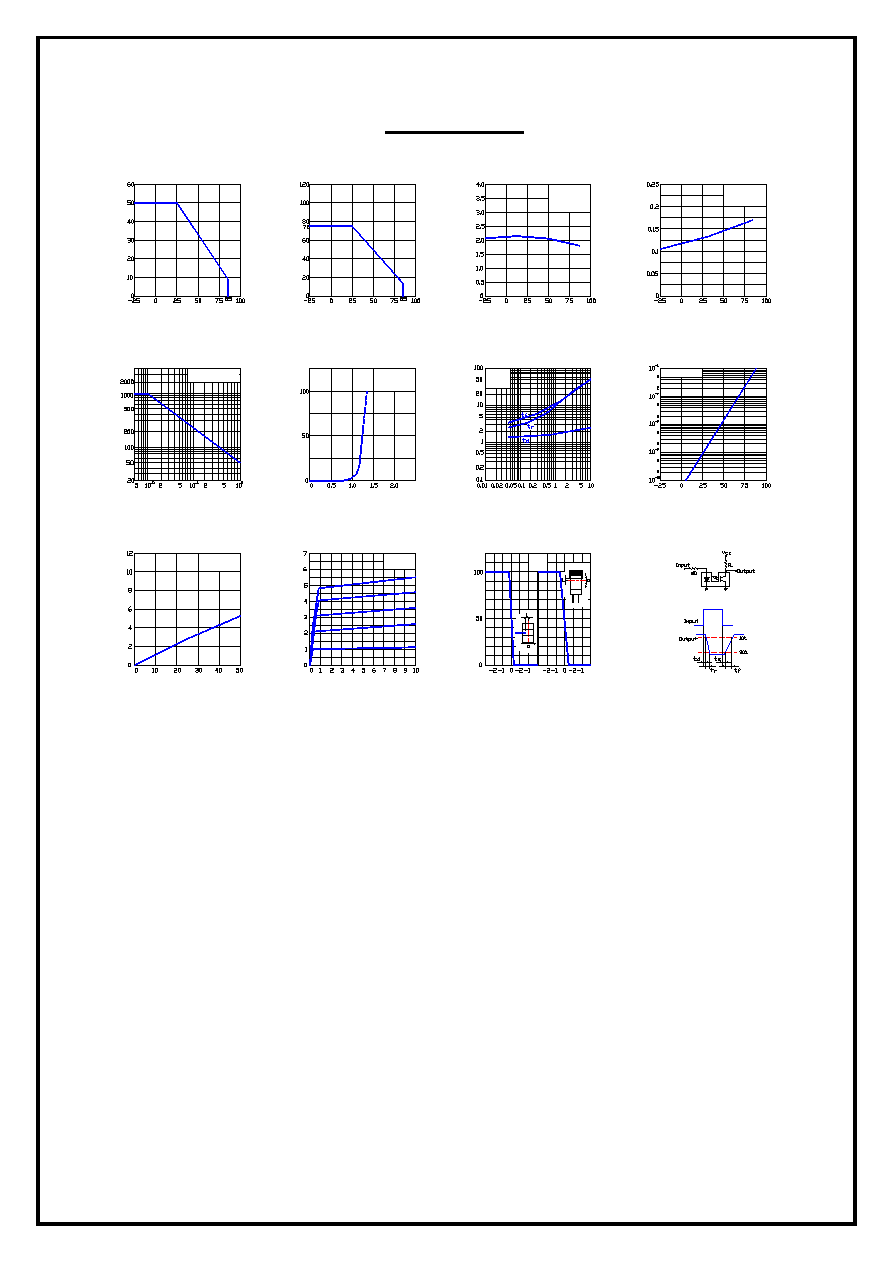
Reference Data
C
o
l
l
e
c
t
o
r
c
u
r
r
e
n
t
I
C
(
mA
)
C
o
l
l
e
c
t
o
r
p
o
w
e
r
d
i
ssi
p
a
t
i
o
n
P
c
(
mW
)
F
o
r
w
a
r
d
c
u
r
r
e
n
t
I
F
(
mA
)
Fig.4 Forward Current vs.
Forward Voltage
Fig.6 Collector Current vs.
Collector-Emitter Voltage
C
o
l
l
e
c
t
o
r
c
u
r
r
e
n
t
I
C
(
mA
)
C
o
l
l
e
c
t
o
r
c
u
r
r
e
n
t
I
C
(
mA
)
Forward current I
F
(mA)
Fig.5 Collector Current vs.
Forward Current
Fig.3 Peak Forward Current vs.
Duty Ratio
P
e
a
k
f
o
r
w
a
r
d
c
u
r
r
e
n
t
I
FM
(
mA
)
F
o
r
w
a
r
d
c
u
r
r
e
n
t
I
F
(
mA
)
Vce=5V
Ta=25
Duty ratio
Pulse width 100s
Ta=25
Ambient temperature Ta ()
R
El
a
t
i
v
e
C
o
l
l
e
c
t
o
r
c
u
r
r
e
n
t
I
c
e
o
(
%
)
Collector-Emitter voltage Vce (V)
Shield distance L (mm)
Forward voltage V
F
(V)
Ta=25
Ambient temperature Ta ()
Ta=25
R
e
s
p
o
n
se
t
i
me
(
s)
Load resistance R
L
(K)
I
F
=20mA
Vce=5V
Ta=25
Fig.11 Relative Collector Current vs.
Shield Distance
X
Y
Ambient temperature Ta ()
Fig.9 Response Time vs.
Load Resistance
Vce=2V
Ic=2mA
Ta=25
Fig.2 Collector Power Dissipation vs.
Ambient Temperature
Fig.1 Forward Current vs.
Ambient Temperature
Fig.7 Collector Current vs.
Ambient Temperature
I
F
=20mA
Vce=5V
C
o
l
l
e
c
t
o
r
-
Emi
t
t
e
r
sa
t
u
r
a
t
i
o
n
v
o
l
t
a
g
e
V
c
e
(
s
at)
(
V
)
C
o
l
l
e
c
t
o
r
d
a
r
k
c
u
r
r
e
n
t
I
c
e
o
(
A
)
Ambient temperature Ta ()
Test Circuit for Response Time
Ambient temperature Ta ()
Fig.10 Collector Dark Current vs.
Ambient Temperature
Vce=20V
Fig.8 Collector-Emitter Saturation Voltage vs.
Ambient Temperature
I
F
=40mA
Ic=0.5mA