DD
0.4
3.0
DD
0.6
Max.
Input Voltage
V
-0.3
+ 0.3
V
ELECTRICAL CHARACTERISTICS
V
Symbol
Controller
LCD
KS0066
or Eqv.
LED Backlight
V
DB7
LEDK
LEDA
RS
R/W
DB0
E
LSI
Storage Temp.
Operating Temp.
LCD Driving Voltage
Supply Current
Output High Voltage
Output Low Voltage
Input Low Voltage
Input High Voltage
BLOCK DIAGRAM
O
DD
SS
V
V
Item
40 SEG
= 1.2mA
= - 0.2mA
-20
( V
-30
OL
V
I
OL
V
16 COM
- V
DD
DD
I
O
Ta=25
= 5.0V
DD
C
OH
IL
V
V
OH
IH
V
I
T
T
stg
opr
I
Condition
Test
--
--
0
--
LCD PANEL
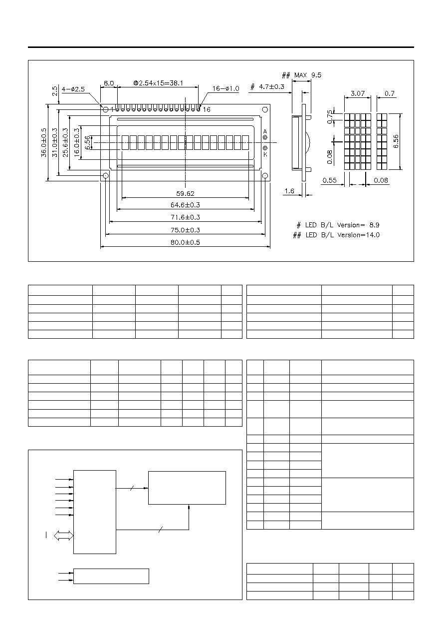
8 Characters x 1 Line
--
--
4.6
1.2
--
=5V
�
0.25V )
2.2
2.4
- 0.3
Min.
DD
--
--
--
Typ.
V
V
70
80
DD
ABSOLUTE MAXIMUM RATINGS
Supply Voltage(LCD)
Supply Voltage(Logic)
Item
LC1611
-0.3
-0.3
Min.
Symbol
DD
DD
V
V
- V
- V
O
SS
13.0
7.0
Max.
16 characters x 1 line
Character Size ( W x H )
V
3.07 x 6.56
mm
LED BACKLIGHT SPECIFICATIONS (Ta=25
In 8-bit bus mode, used as high
order bidirectional data bus.
In 4-bit bus mode, used as both
high and low order data bus.
Power supply for LED backlight
In 8-bit bus mode, used as low
order bidirectional data bus.
In 4-bit bus mode, open these
pins.
Operating voltage for LCD
L : Write
Enable signal
L : Instruction code
Power supply for logic
H : Data
H : Read
Approx. 26 / 36
0.55 x 0.75
DB6
Forward Voltage
Emission Wave Length
Forward Current
DB7
LEDA
LEDK
Item
15
16
13
14
f
I
p
+5V
0V
H/L
H/L
Symbol
V
f
DB4
DB5
SS
R/W
DB1
DB2
DB3
DB0
RS
O
DD
Weight (Reflective/LED)
Dot Size ( W x H )
PIN CONNECTIONS
Symbol
V
mA
V
7
10
11
12
8
9
5
6
4
E
V
V
V
Unit
C
C
2
3
1
Pin
V
V
V
>L
_
H/L
H/L
H/L
H/L
H/L
H/L
H/L
H,H
H/L
+5V
Level
0V
--
GND
V
nm
mA
Unit
120
--
568
--
4.1
Typ.
Max.
4.3
C)
mm
Function
g
80.0 x 36.0 x 9.5/14.0
Nominal Dimensions
64.6 x 16.0
MECHANICAL DATA
Viewing Area ( W x H )
Module Size ( W x H x T )
V
Unit
V
Item
mm
mm
Unit