 | –≠–ª–µ–∫—Ç—Ä–æ–Ω–Ω—ã–π –∫–æ–º–ø–æ–Ω–µ–Ω—Ç: LC549 | –°–∫–∞—á–∞—Ç—å:  PDF PDF  ZIP ZIP |
LC549/LV549/LD549 DATA SHEET
High Power Class B
Output Stage
FEATURES
∑
40dB of electrical gain
∑
1.0 to 1.6 VDC supply operating range
∑
current trim capability (R
T
)
∑
high efficiency class B output stage
∑
may be used with a linear or compression preamplfier
STANDARD PACKAGING
∑ 8 pin MICROpac (LC549)
∑ 8 pin MINIpac
∑ 8 pin PLID
Æ
(LC549, LD549)
∑ Chip (47 x 40 mils) (LC549, LD549)
DESCRIPTION
The LC/LV/LD549 is an 8 pin, low voltage, push-pull audio
frequency output stage amplifier with a single unbalanced
input. The circuit utilizes two internal negative feedback
loops to stabilize the DC operating point for temperature
stability and to linearize the transfer function over a wide
dynamic range. The circuit operates near ideal class B
conditions resulting in low distortion and very low quiescent
current, required for extended battery life.
The LC549, LV549 and LD549 differ in only one respect;
the LV549 and LD549 are selected devices which are
capable of delivering from 10 mA to 41 mA and from 36 mA
to 75 mA of output current respectively. These values are
the maximum current drawn with both output stage transistors
in saturation. Thus the LD549 is capable of producing a
high output in a low impedance load, the LV549 is selected
to have lower peak currents, extending the life of the
battery.
U.S. Patent No. 4,085,382
Patented in other countries
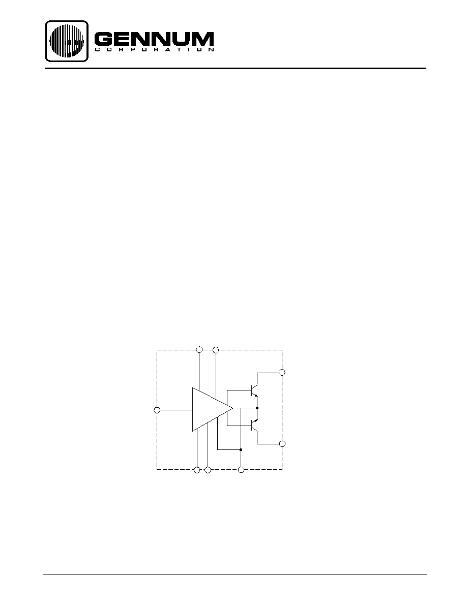
BLOCK DIAGRAM
4
3
2
7
1
6
5
8
R
T
V
B
OUTPUT 1
OUTPUT 2
INPUT
DEC 1 DEC 2
GND
GENNUM CORPORATION P.O. Box 489, Stn A, Burlington, Ontario, Canada L7R 3Y3 tel. (905) 632-2996 fax: (905) 632-5946
Japan Branch: A-302 Miyamae Village, 2-10-42 Miyamae, Suginami-ku Tokyo 168, Japan tel. (03) 3334-7700 fax: (03) 3247-8839
Document No. 500 - 25 - 09
Revision Date: January 2001

2
500 - 25 - 09
SEQUENCE CONDITIONS COMMENTS
1
Power Supply
Off
2
S1
Closed
Removes V
IN
3
S2 / S3
Closed
Discharges C2 and C3
4
S1
Open
Applies V
IN
(V
IN
level is determined from Gain Test)
5
S2 / S3
Open
Removes short from C2 and C3
6
Power Supply
On
7
Gain must be within specification, within 3 seconds after power supply is turned on
ABSOLUTE MAXIMUM RATINGS
PARAMETER
VALUE & UNITS
Supply Voltage
3 VDC
Power dissipation
60 mW
Operating Temperature
-10 to + 40
∞
C
Storage Temperature
-20 to + 70
∞
C
CAUTION
CLASS 1 ESD SENSITIVITY
1
4
5
8
PIN CONNECTION
DEC1
R
T
I/P
DEC2
V
B
GND
OUT1
OUT2
ELECTRICAL CHARACTERISTICS
Conditions: Temperature 25
o
C, Supply Voltage V
B
= 1.3 VDC
All switches and parameters remain as shown in test circuit unless stated in condition column
PARAMETER SYMBOL
CONDITION MIN TYP
MAX
UNITS
Gain
A
CL
V
OUT
= 0.707 V
RMS
38
40
42
dB
Quiescent Current
I
AMP
100
-
400
µ
A
I
TRANS
170
-
370
µ
A
I
TOT
-
500
770
µ
A
Maximum Drive Current
V1 = 0V (S2, S3 closed)
V4 = 0V LC549
10
35
75
mA
LV549
10
-
41
mA
LD549
36
50
75
mA
Input Impedance
18
27
36
k
Total Harmonic Distortion & Noise
THD
V
OUT
= 0.707 V
RMS
-
0.5
-
%
V
OUT
= 1.3 V
RMS
-
2.5
5.2
%
Input Referred Noise
IRN
NFB 0.2 to 10 kHz at 12 dB/oct (S1 closed)
-
1.2
2.5
µ
V
Start Up Time
-
-
3
sec
START-UP TIME TEST (Refer to Test Circuit)
3
500 - 25 - 09
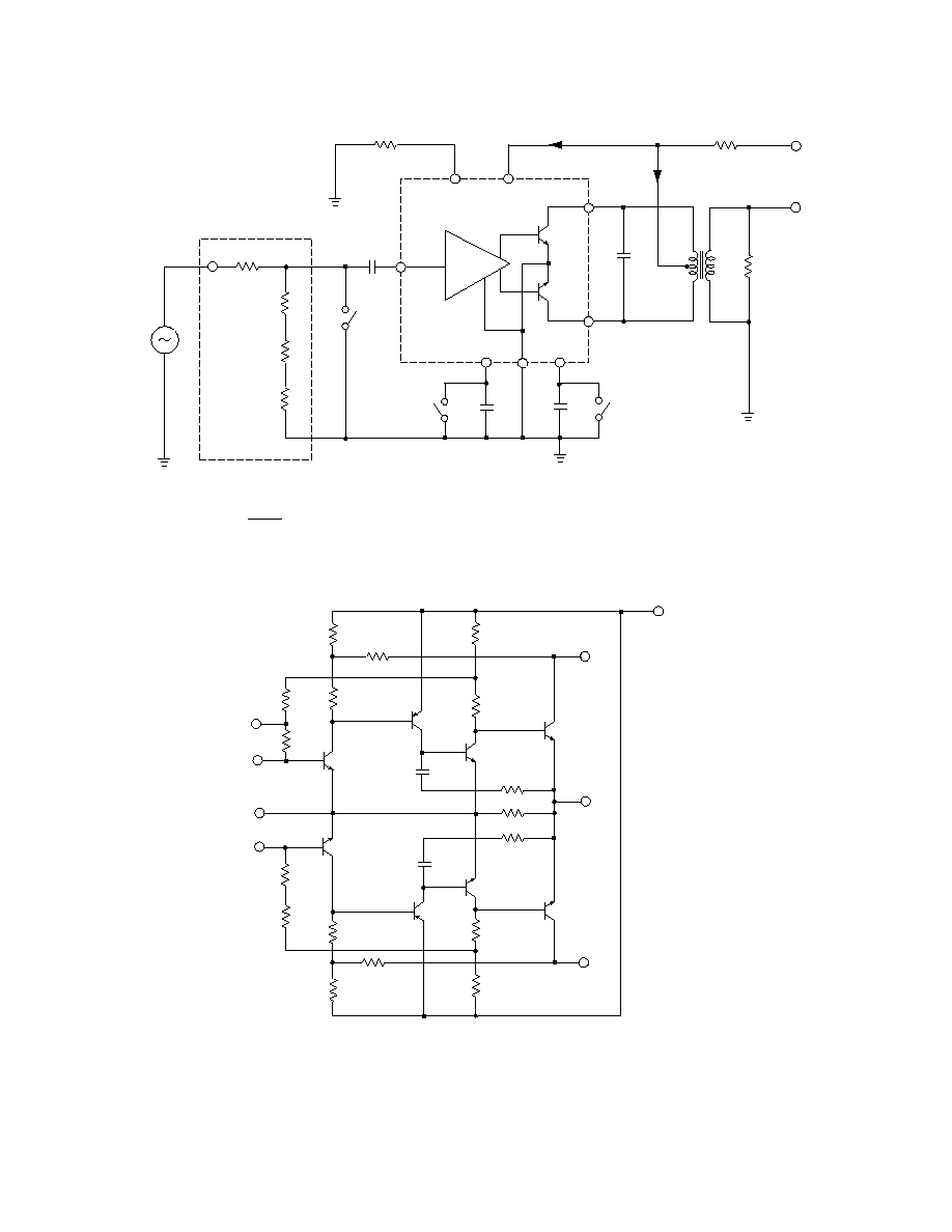
Fig. 1 Test Circuit
All resistors in ohms, all capacitors in farads unless otherwise stated
U.S. Patent No. 4,085,382 - Patented in other countries
Fig. 2 Equivalent Circuit
C4
0.047
C2
6.8
C3
6.8
V
B=
1.3VDC
R
L
400
R
T=
I
TRANS
LC/LD549
600
1kHz
V
IN
60k
560
S1
S2
S3
C1
0.1
39
10
40dB ATTENUATOR
V
OUT
TI
1:1
4
3
2
7
1
6
5
8
I
AMP
All resistors in ohms, all capacitors in
µ
F unless otherwise stated
Gain = 20 Log
10
( ) +40 dB
VOUT
VIN
1
2
4
3
6
8
+
+
600
27k
5
7
=
4
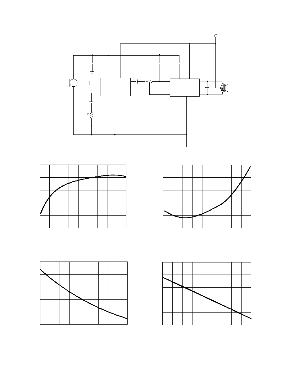
500 - 25 - 09
6.8
470 TYP
.0.047
+
+
+
V
B=
1.3VDC
V
C=
10k
G
T
10k
LC506
LC/LD549
2.2
0.1
0.01
NC
4
4
3
3
2
2
7
1
1
6
6
5
5
8
MIC
6.8
6.8
TEMPERATURE
∞
C
Fig. 4 Volume Gain vs Battery Voltage
Fig. 5 Quiescent Current vs Battery Voltage
Fig. 6 Quiescent Current vs Temperature
Fig. 7 Gain vs Temperature
-20 -10 0 10 20 30 40 50 60 70
41.0
40.2
39.4
38.6
37.8
37.0
46
44
42
40
38
36
A
V
(dB)
V
B
(V)
V
B
(V)
I
Q
(
µ
A)
I
Q
(
µ
A)
-20 -10 0 10 20 30 40 50 60 70
TEMPERATURE (
∞
C)
A
V
(dB)
All resistors in ohms, all capacitors in farads unless otherwise stated
Fig. 3 Typical Hearing Aid Circuit
800
700
600
500
400
300
0.9 1.0 1.1 1.2 1.3 1.4 1.5 1.6 1.7 1.8
532
524
516
508
500
492
0.9 1.0 1.1 1.2 1.3 1.4 1.5 1.6 1.7 1.8
5
500 - 25 - 09
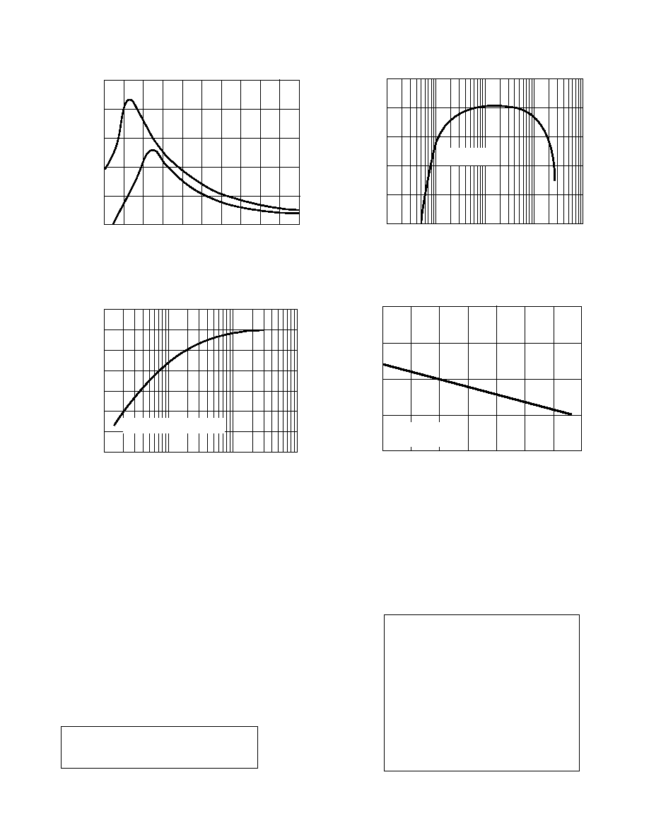
RELATIVE VOLTAGE GAIN (dB)
Gennum Corporation assumes no responsibility for the use of any circuits described herein and makes no representations that they are free from patent infringement.
© Copyright January 1981 Gennum Corporation. All rights reserved. Printed in Canada.
REVISION NOTES
Changes to standard packaging information
POWER OUTPUT (mV)
I
Q
(
µ
A)
A
V
(dB)
V
OUT
=0.707 V
RMS
V
OUT
=0.707 V
RMS
V
B
=1.3 V
THD<5.2% AT V
OUT
=1.3 V
RMS
0 4 8 12 16 20 24 26
0.0
1 0.1 1.0 10 100
12
10
8
6
4
2
LD
LC
-0 200 400 600 800 1k
41
40
39
38
37
36
40.4
40.2
40.0
39.8
39.6
550
500
450
400
350
300
250
200
LOAD R
L
(
)
FREQUENCY (kHZ)
Fig. 9 Voltage Gain vs Frequency
Fig. 8 Power Output vs Load Resistance
at 7% Distortion R
B
= 0
1
10 100 1K
SUPPLY VOLTAGE (V)
Fig. 11 Voltage Gain vs Battery Resistance
Fig. 10 Quiescent Current vs Current Trim Resistor
R
T
(k
)
DOCUMENT IDENTIFICATION
PRODUCT PROPOSAL
This data has been compiled for market investigation purposes
only, and does not constitute an offer for sale.
ADVANCE INFORMATION NOTE
The product is in a development phase and specifications are
subject to change without notice. Gennum reserves the right to
remove the product at any time. Listing the product does not
constitute an offer for sale.
PRELIMINARY DATA SHEET
The product is in preproduction phase and specifications are
subject to change without notice.
DATA SHEET
The product is in production. Gennum reserves the right to make
changes at any time to improve reliability, function or design, in
order to provide the best product possible.