 | ÐлекÑÑоннÑй компоненÑ: LD1010D | СкаÑаÑÑ:  PDF PDF  ZIP ZIP |
Äîêóìåíòàöèÿ è îïèñàíèÿ www.docs.chipfind.ru

PWRLITE LD1010D
High Performance N-Channel
P
OWERJFET
TM
with PN Diodes
Features
Trench Power JFET with low threshold voltage Vth.
Device fully "ON" with Vgs = 0.7V
Optimum for "Low Side" Buck Converters
Optimized for Secondary Rectification in isolated DC-DC
Low Rg and low Cds for high speed switching
No "Body Diode"; extremely low Cds
Added Fast Recovery Schottky Diode in same package
Applications
DC-DC Converters
Synchronous Rectifiers
PC Motherboard Converters
Step-down power supplies
Brick Modules
VRM Modules
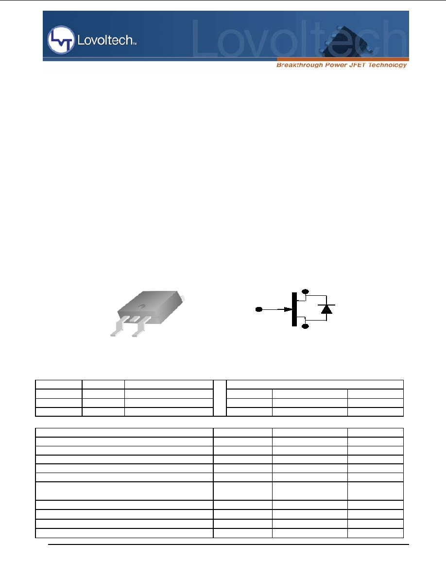
DPAK Pin Assignments
Description
The Power JFET transistor from Lovoltech is a device that
presents a Low Rdson allowing for improved efficiencies in DC-
DC switching applications. The device is designed with a low
threshold such that drivers can operate at 5V, which reduces the
driver power dissipation and increases the overall efficiency.
Lower threshold produces faster turn-on/turn-off, which
minimizes the required dead time. The transistor "No Body
Diode" provides a very low associated parasitic capacitance Cds.
A Schottky Diode is added for applications where a freewheeling
diode is required. Ringing is also reduced so that a lower voltage
device may be a better solution.
G
S
D
S
D
G
N Channel Power JFET
with PN Diode
G
S
D
G
S
D
S
D
G
N Channel Power JFET
with PN Diode
S
D
G
N Channel Power JFET
with PN Diode
Pin Definitions
Pin Number
Pin Name
Pin Function Description
Product Summary
1 Gate
Gate. Transistor Gate
V
DS
(V)
Rdson (
)
I
D
(A)
2 Drain
Drain. Transistor Drain 24V 0.0045
50
3 Source
Source. Transistor Source
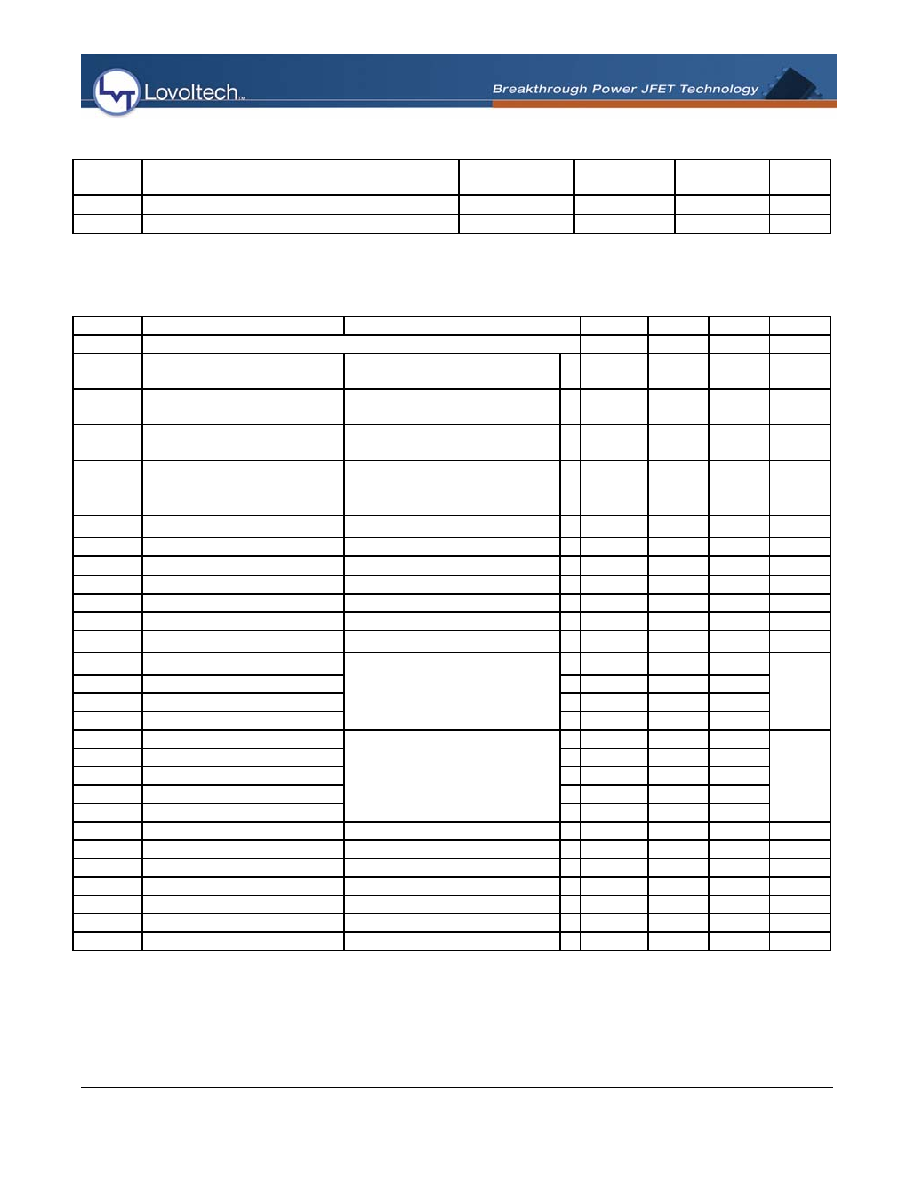
Absolute Maximum Ratings
Parameter Symbol
Ratings
Units
Drain-Source Voltage
V
DS
24
V
Gate-Source Voltage
V
GS
-10 V
Gate-Drain Voltage
V
GD
-28 V
Continuous Drain Current
I
D
50 A
Pulsed Drain Current
I
D
100 A
Single Pulse Drain-to-Source Avalanche Energy at 25
°C
(V
DD
= 5V
DC
, IL=60A
PK
, L=0.3mH, R
G
=100
)
E
AS
220 mJ
Junction Temperature
T
J
-55 to 150
°C
°C
Storage Temperature
T
STG
-65 to 150
°C
°C
Lead Soldering Temperature, 10 seconds
T
260
°C
°C
Power Dissipation (Derated at 25
°C)
P
D
80 W
LD1010D.Rev
1.2
12-04

Thermal Resistance
Symbol Parameter
DPAK
Ratings
Units
R
JA
Thermal Resistance Junction-to-Ambient
80
°C/W
R
JC
Thermal Resistance Junction-to-Case
1.6
°C/W
Electrical Specifications
(TA = +25°C, unless otherwise noted.)
The
denotes a specification which apply over the full operating temperature range.
Symbol Parameter
Conditions
Min.
Typ.
Max.
Units
Static
BV
DSX
Breakdown
Voltage
Drain to Source
I
D
= 0.5 mA
V
GS
= -4 V
24
V
BV
GDO
Breakdown
Voltage
Gate to Drain
I
G
= -50
µA
-28 V
BV
GSO
Breakdown
Voltage
Gate to Source
I
G
= -1 mA
-12
-10
V
R
DS(ON
)
Static Drain to Source
1
On
Resistance (Current flows
drain-to-source) See Fig. 1
I
G
= 40 mA, I
D
=10A
I
G
= 10 mA, I
D
=10A
I
G
= 5 mA, I
D
=10A
4.0
4.5
4.6
4.5
5.0
m
m
V
GS(TH)
Gate
Threshold
Voltage
V
DS
=0.1 V, I
D
=250
µA
-1200 -800 -600 mV
Dynamic
Q
G
Total Gate Charge
V
Drive
=5V, I
D
=10A,V
DS
=15V
20 nC
Q
GD
Gate to Drain Charge
12
nC
Q
GS
Gate to Source Charge
1.5
nC
Q
SW
Switching
Charge
13.5 nC
R
G
Gate
Resistance
0.4
T
D(ON
) Turn-on
Delay
Time
5
T
R
Rise
Time
12
T
D(OFF)
Turn-off
Delay
2
T
F
Fall
Time
V
DD
=16V, I
D
=15A
V
Drive
= 5 V
Clamped Inductive Load
10
ns
C
ISS
Input
Capacitance
3000
C
OSS
Output
Capacitance
900
C
GS
Gate-Source
Capacitance
2250
C
GD
Gate-Drain
Capacitance
750
C
DS
Drain-Source
Capacitance
V
DS
=10V, V
GS
= -5 V, 1MHz.
150
pF
PN Diode
I
R
Reverse
Leakage
V
R
=20V, Vgs = -4V
0.25
0.3
mA
V
F
Forward
Voltage
I
F
= 1 A
700
mV
V
F
Forward
Voltage
I
F
= 10 A
900
mV
V
F
Forward
Voltage
I
F
= 20 A
1100
mV
Qrr
Reverse Recovery Charge
I
s
= 20 A di/dt = 100A/us,
20
nC
Notes:
1.
Pulse width <= 500
µs, duty cycle < = 2%
Lovoltech, Inc. - 3970 Freedom Circle - Santa Clara, CA 95054 -USA
Tel. 1 408 654 1980 Fax 1 408 654 1988 www.lovoltech.com
LD1010D
Product Specification
2

Typical Operating Characteristics
(TA = +25°C, unless otherwise noted.)
RDS(ID=-10A) vs IG, at Room Temperature.
0.0030
0.0032
0.0034
0.0036
0.0038
0.0040
0.0042
0.0044
0.0046
0.0048
0.0050
0.0052
0.0054
0.0056
0.001
0.010
0.100
1.000
IG(A)
RDS(
O
h
m
s
)
RDS(ID=-10A) vs IG, at Room Temperature.
0.0030
0.0032
0.0034
0.0036
0.0038
0.0040
0.0042
0.0044
0.0046
0.0048
0.0050
0.0052
0.0054
0.0056
0.001
0.010
0.100
1.000
IG(A)
RDS(
O
h
m
s
)
Total Gate Charge curves
-5
-4
-3
-2
-1
0
1
2
0
10
20
30
40
5
QtotG(nC)
VG
S(
V
)
DC Charges Region
Capacitive
Charges
Region
Total Gate Charge curves
-5
-4
-3
-2
-1
0
1
2
0
10
20
30
40
5
QtotG(nC)
VG
S(
V
)
DC Charges Region
Capacitive
Charges
Region
0
0
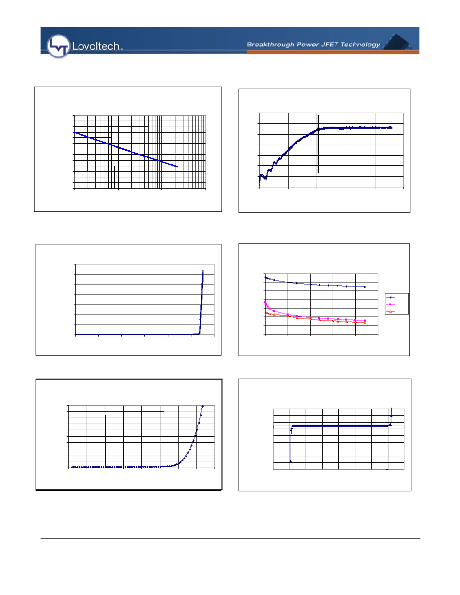
Figure 1 R
DSON
vs Gate Current at I
D
10A
Figure 2 Total Gate Charge
Capacitance vs VDS, VGS=-4V
at Room Temp
0
500
1000
1500
2000
2500
3000
3500
0
5
10
15
20
25
VDSV)
C
(
pF)
Ciss
Coss
Crss
BVgs plot: Id vs Vds for Vgs=-4V
0.00E+00
2.00E-04
4.00E-04
6.00E-04
8.00E-04
1.00E-03
1.20E-03
1.40E-03
0
5
10
15
20
25
30
Vds(V)
Id
(
A
)
Figure 3 Breakdown Voltage Vds vs Id
Figure 4 Capacitance vs Drain Voltage Vds
IG vs VGS, Drain Open
Room Temp
-1.3E-03
-1.1E-03
-9.0E-04
-7.0E-04
-5.0E-04
-3.0E-04
-1.0E-04
1.0E-04
3.0E-04
5.0E-04
-14
-12
-10
-8
-6
-4
-2
0
2
VGSV)
IG
(A
)
IG vs VGS, Source and Drain Grounded.
At Room Temperature
0.E+00
1.E-02
2.E-02
3.E-02
4.E-02
5.E-02
6.E-02
7.E-02
8.E-02
9.E-02
1.E-01
0.0
0.1
0.2
0.3
0.4
0.5
0.6
0.7
0.8
VGS(V)
IG
(
A
)
IG vs VGS, Source and Drain Grounded.
At Room Temperature
0.E+00
1.E-02
2.E-02
3.E-02
4.E-02
5.E-02
6.E-02
7.E-02
8.E-02
9.E-02
1.E-01
0.0
0.1
0.2
0.3
0.4
0.5
0.6
0.7
0.8
VGS(V)
IG
(
A
)
Figure 5 I
G
vs Gate Voltage V
GS
Figure 6 Typical Gate Voltage
Characteristic
Lovoltech, Inc. - 3970 Freedom Circle - Santa Clara, CA 95054 -USA
Tel. 1 408 654 1980 Fax 1 408 654 1988 www.lovoltech.com
LD1010D
Product Specification
3

Typical Operating Characteristics
(TA = +25°C, unless otherwise noted.)
Normalized Rdson vs Temp at ID=-20A
1.00
1.10
1.20
1.30
1.40
1.50
1.60
1.70
1.80
1.90
2.00
0
20
40
60
80
100
120
140
Temp(C)
N
o
r
m
al
i
z
ed
R
d
so
n
0.0
5.0
10.0
15.0
20.0
25.0
0
0.025
0.05
0.075
0.1
Vds, Drain-to-Source Voltage (V)
Id
,
Drai
n
C
u
r
r
e
n
t
(A
)
IG=1mA
IG=5mA
IG=10mA
IG=20mA
IG=40mA
IG=100mA
0.0
5.0
10.0
15.0
20.0
25.0
0
0.025
0.05
0.075
0.1
Vds, Drain-to-Source Voltage (V)
Id
,
Drai
n
C
u
r
r
e
n
t
(A
)
IG=1mA
IG=5mA
IG=10mA
IG=20mA
IG=40mA
IG=100mA
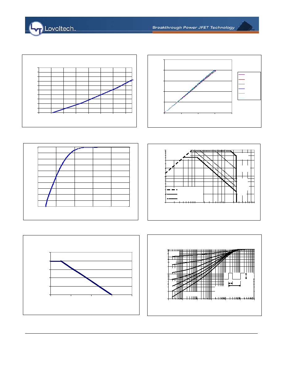
Figure 7 R
DSON
Temperature Coefficient
Figure 8 On-Region Characteristics
1
10
100
0.1
1
10
100
Vds, Drain-to-Source Voltage (V)
I
d
,
Dr
a
i
n
Cu
r
r
e
n
t
(
A
)
Rdson Limit
Thermal Limit
Package Limit
100
µs
1ms
DC
10
µs
10ms
Ig = 40mA
Single Pulse
Tc = 25
°C
1
10
100
0.1
1
10
100
Vds, Drain-to-Source Voltage (V)
I
d
,
Dr
a
i
n
Cu
r
r
e
n
t
(
A
)
Rdson Limit
Thermal Limit
Package Limit
100
µs
1ms
DC
10
µs
10ms
Ig = 40mA
Single Pulse
Tc = 25
°C
-20
-18
-16
-14
-12
-10
-8
-6
-4
-2
0
-1.00
-0.90
-0.80
-0.70
-0.60
-0.50
VDS (Volts)
ID
(A
m
p
s)
Figure 9 Diode Voltage vs Current
Figure 10 Safe Operating Area
ZthJA = f(tp) (parameter D= tp/T)
1.E-02
1.E-01
1.E+00
1.E-05
1.E-04
1.E-03
1.E-02
1.E-01
1.E+00
1.E+01
tp (s)
Zt
hJ
A
(
K
/
W
)
D = 0.5
0.2
0.1
0.05
0.02
0.01
Single Pulse
Note:
1.
Duty Factor D = tp/T
2.
Peak Tj = P(pk)*Z
thJA
+ T
A
T
tp
P(pk)
ZthJA = f(tp) (parameter D= tp/T)
1.E-02
1.E-01
1.E+00
1.E-05
1.E-04
1.E-03
1.E-02
1.E-01
1.E+00
1.E+01
tp (s)
Zt
hJ
A
(
K
/
W
)
D = 0.5
0.2
0.1
0.05
0.02
0.01
Single Pulse
Note:
1.
Duty Factor D = tp/T
2.
Peak Tj = P(pk)*Z
thJA
+ T
A
T
tp
P(pk)
D = 0.5
0.2
0.1
0.05
0.02
0.01
Single Pulse
Note:
1.
Duty Factor D = tp/T
2.
Peak Tj = P(pk)*Z
thJA
+ T
A
T
tp
P(pk)
T
tp
P(pk)
T
tp
P(pk)
Total Pow er Dissipation (W)
0.00
20.00
40.00
60.00
80.00
100.00
0
50
100
150
200
Te m pe rature (C)
Pt
o
t
(
W
)
Total Pow er Dissipation (W)
0.00
20.00
40.00
60.00
80.00
100.00
0
50
100
150
200
Te m pe rature (C)
Pt
o
t
(
W
)
Figure 11 Total Power Dissipation Figure 12 Normalized Thermal Response
Lovoltech, Inc. - 3970 Freedom Circle - Santa Clara, CA 95054 -USA
Tel. 1 408 654 1980 Fax 1 408 654 1988 www.lovoltech.com
LD1010D
Product Specification
4

Ordering Information
Product Number
PN Marking Package
LD1010D LD1010D
TO252
(DPAK)
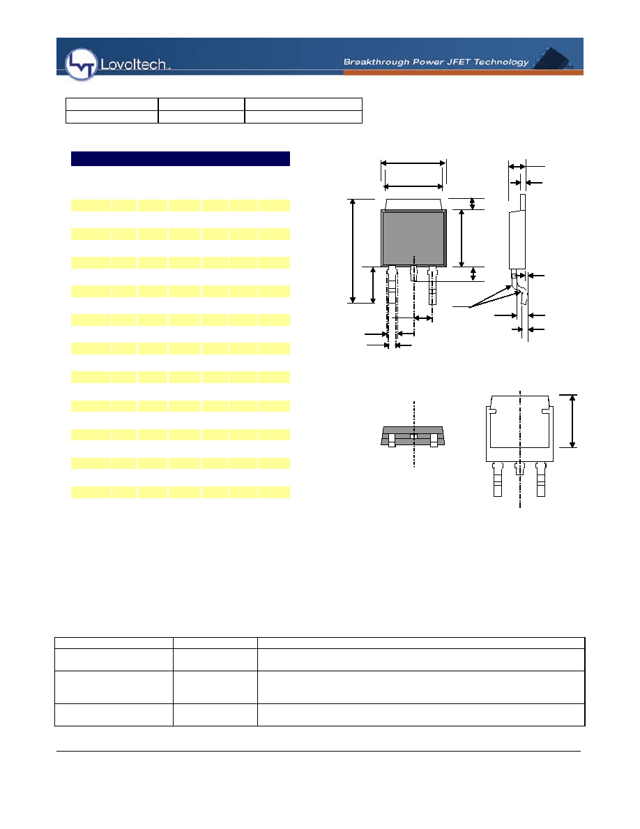
Package and Marking Information:
DIMENSIONS
mm.
inch
DIM.
TYP.
MIN.
MAX.
TYP.
MIN.
MAX.
A
2.19
2.40
0.086
0.094
A1
0.89
1.14
0.035
0.045
A2
0.03
0.13
0.001
0.005
b
0.76
1.14
0.030
0.045
b1
0.55
0.90
0.022
0.035
B2
5.20
5.46
0.205
0.215
C
0.45
0.60
0.017
0.023
C2
0.45
0.58
0.017
0.023
D
5.97
6.22
0.235
0.245
D1
5.30
0.208
E
6.35
6.73
0.250
0.265
e
2.28
0.090
H
9.35
10.42
0.368
0.410
L2
0.88 1.27
0.035 0.050
L3
1.86 3.57
0.073 0.140
L4
0.64
1.02
0.025
0.040
R
0.20
0.008
Alternate
D
5.40
5.60
0.213
0.220
L2
1.25 1.75
0.049 0.069
L3
2.60 2.80
0.102 0.110
H
9.65
9.75
0.380
0.384
H
H
H
A1
C2
A
C
R
A2
DP
A
K
D
E
B2
L3
e
b1
b
L4
L2
LD1010D
AXXXXX
XXXX
A1
C2
A
C
R
A2
DP
A
K
A1
C2
A
C
R
A2
DP
A
K
D
E
B2
L3
e
b1
b
L4
L2
LD1010D
AXXXXX
XXXX
D
E
B2
L3
e
b1
b
L4
L2
LD1010D
AXXXXX
XXXX
D1
Back View
D1
Back View
Life Support Policy
LOVOLTECH's PRODUCTS ARE NOT AUTHORIZED FOR USE AS CRITICAL COMPONENTS IN LIFE SUPPORT DEVICES
OR SYSTEMS WITHOUT THE EXPRESS WRITTEN APPROVAL OF THE PRESIDENT OF LOVOLTECH, Inc. As used herein:
1. Life support devices or systems are devices or systems which (a) are intended for surgical implant into the body, or (b) support or
sustain life, and (c) whose failure to perform when properly used in accordance with instructions for use provided in the labeling can
be reasonably expected to result in a significant injury of the user.
2. A critical component in any component of a life support device or system whose failure to perform can be reasonably expected to
cause the failure of the life support device or system, or to affect its safety or effectiveness.
Datasheet Identification
Product Status
Definition
Advance Information
In definition or in
Design
This datasheet contains the design specifications for product development.
Specifications may change without notice.
Preliminary
Initial Production
This datasheet contains preliminary data; additional and application data will be
published at a later date. Lovoltech, Inc. reserves the right to make changes at any
time without notice in order to improve design.
No Identification Needed
In Production
This datasheet contains final specifications. Lovoltech reserves the right to make
changes at any time without notice in order to improve the design.
Lovoltech, Inc. - 3970 Freedom Circle - Santa Clara, CA 95054 -USA
Tel. 1 408 654 1980 Fax 1 408 654 1988 www.lovoltech.com
LD1010D
Product Specification
5
Document Outline
