Äîêóìåíòàöèÿ è îïèñàíèÿ www.docs.chipfind.ru
Bay Linear, Inc
2478 Armstrong Street, Livermore, CA 94550 Tel: (925) 989-7144, Fax: (925) 940-9556 www.baylinear.com
100mA Low Dropout Voltage Regulator
LM2931
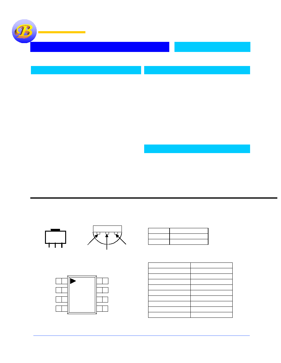
Pin Connection
Ordering Information
8SOIC (M)
Package Tolerance
SOT-89
LM2931R-XX
TO-92
LM2931Z-XX
8-SOIC
LM2931M-XX
"XX" Voltage Selection Guide
Vout
XX Code
3.3V
33
5.0V
50
8.0V
80
8.5V
85
9.0V
90
10.0V
10
12.0V
12
15.0V
15
Adjustable
Left Blank
Description
The Bay Linear LM2931 are low power voltage regulators
designed for a wide range of applications. They are an
excellent choice for use in Battery Powered applications. The
LM2931 feature low quiescent current (100
µ
A Typ.) and low
dropout of only 60mV at light loads and 300mV (typ.) at
100mA. The LM2931 has tight initial tolerance of 0.5% typ.,
extremely good load and line regulation of 0.05% typ. and very
low output temperature coefficient.
The Bay Linear LM2931 is available as a fixed voltage
regulator and as an adjustable regulator in TO-92 and 8SOIC
packages. The Bay Linear LM2931 in an 8SOIC package has
an adjustable output voltage from 3V to 24V, programmed
with a pair of external resistor. The logic compatible shutdown
enables the regulator to be switched ON and OFF.
Features
·
Guaranteed 100mA Output
·
Fixed Versions 3.3V, 50.V, 8.0
·
Very Low Quiescent Current
·
Low Dropout Voltage
·
Extremely Tight Load and Line
Regulation
·
Very Low Temperature Coefficient
·
Current and Thermal Limiting
·
Reverse Battery Protection of 20V
·
Transient protection of 60V
·
Output programmable from 3V to 24V
Applications
·
Battery Powered Systems
·
Portable instrumentation
·
Notebooks Computers
·
Potable Consumer Equipment
·
Automotive electronics
·
SMPS Post-Regulator
Bay Linear
Bay Linear
Bay Linear
Bay Linear
Linear Excellence
1
2
4
3
5
6
7
8
Output
Input
GND
GND
GND
GND
Feedback
Shutdown
SOT-89
Front View
INPUT
GND OUTPUT
BAY
LM2931
OUTPUT
GROUND
INPUT
1
3
2
TO-92
Bottom View
SOT-89
Front View
INPUT
GND OUTPUT
BAY
LM2931
SOT-89
Front View
INPUT
GND OUTPUT
BAY
LM2931
OUTPUT
GROUND
INPUT
1
3
2
TO-92
Bottom View
OUTPUT
GROUND
INPUT
1
3
2
TO-92
Bottom View
Bay Linear, Inc
2478 Armstrong Street, Livermore, CA 94550 Tel: (925) 989-7144, Fax: (925) 940-9556 www.baylinear.com
LM2931
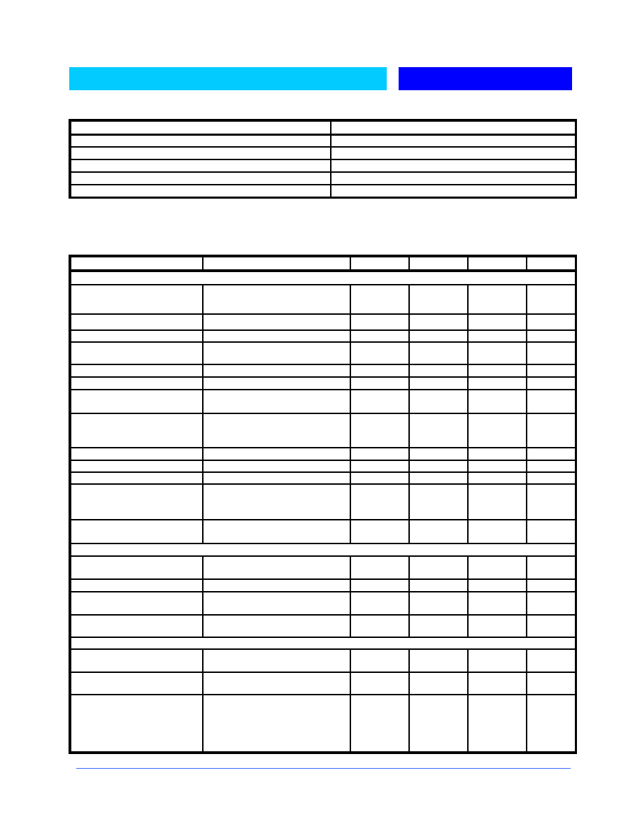
Absolute Maximum Rating
Parameter
Power Dissipation
Internally Limited
Lead Temperature ( Soldering 5 seconds )
260
°
C
Storage Temperature Range
-65
°
C to +150
°
C
Operating Junction Temperature
-55
°
C to +150
°
C
Input Supply Voltage
-20 to +35V
Electrical Characteristics
T
J
= 25
°
C , I
O
= 100
µ
A, V
IN
= 14V ( for 2931-15 V
IN
= 16V), C
O
= 100
µ
F; unless otherwise specified)
Parameter Conditions
MIN
TYP
MAX
UNIT
Output Voltage
(Fixed Version)
-25
°
C
T
j
85
°
C
Full Operating Temperature
0.985 [ V
o
]
0.98 [ V
o
]
V
o
1.015 [ V
o
]
1.02 [ V
o
]
V
Output Voltage (Fixed Version) 100
µ
A
I
L
100mA, T
j
T
jmax
0.975 [V
o
] V
o
1.025 [ V
o
]
V
Input Supply Voltage
26
V
Output Voltage Temperature
Coefficient
(Note 1)
50
150
ppm /
°
C
Line Regulation (Note 2)
13V
V
IN
26V (Note 3)
0.1
0.4
%
Load Regulation (Note 2)
100
µ
A
I
L
100mA
0.1
0.3
%
Dropout Voltage (Note 4)
I
L
= 100
µ
A
I
L
= 100mA
60
300
200
600
mV
Ground Current (Note 5)
I
L
= 100
µ
A
I
L
= 10mA
I
L
= 100mA
100
0.9
8
150
1.5
12
µ
A
mA
mA
Dropout Ground Current
V
IN
= (V
OUT
0.5V), I
L
= 100
µ
A
110
170
µ
A
Current Limit
V
OUT
= 0
160
200
mA
Thermal Regulation (Note 6)
0.05
0.2
% / W
Output Noise,
10Hz to 100KHz
I
L
= 10mA
C
L
= 2.2
µ
F
C
L
= 3.3
µ
F
C
L
= 33
µ
F
500
350
120
µ
Vrms
Ripple Rejection Ratio
I
O
= 10mA, f = 120Hz, C
0
= 100
µ
F
V
IN
= V
O
+ 3V+2Vpp
60
dB
8 pin Versions only (LP2951)
Reference Voltage
Over Temperature (Note 7)
1.21
1.185
1.235 1.26
1.285
V
Feedback Pin Bias Current
20
40
A
Reference Voltage Temperature
Coefficient
(Note 1)
50
ppm/
°
C
Feedback Pin Bias Current
Temperature Coefficient
0.1
A/
°
C
Shutdown Input
Input Logic Voltage
Low (Regulator ON)
High (Regulator OFF)
2
1.3 0.7 V
Shutdown Pin Input Current
V
S
= 2.4V
V
S
= 26V
30
450
50
600
µ
A
Regulator Output Current
in Shutdown
(Note 8)
5.0V
V
OUT
15.0V
3.3V
V
OUT
5.0V
2.0V
V
OUT
3.3V
10
20
30
µ
A

Bay Linear, Inc
2478 Armstrong Street, Livermore, CA 94550 Tel: (925) 989-7144, Fax: (925) 940-9556 www.baylinear.com
LM2931
Note 1: Output or reference voltage temperature coefficients defined as the worst case voltage change divided by the total temperature range.
Note 2: Unless otherwise specified all limits guaranteed for T
J
= 25
°
C, V
IN
= V
O
+1V, I
L
= 100
µ
A and C
L
= 1
µ
F. Additional conditions for the 8-
pin versions are feedback tied to XX Voltage tap and output tied to output Sense pin ( V
OUT
= XX V) and V
SHUTDOWN
0.8V
Note 2: Regulation is measured at constant junction temperature , using pulse testing with a low duty cycle. Changes in output voltage due to
heating effects are covered under specification for thermal regulation.
Note 3: Line regulation for is tested at 150
°
C for I
L
= 1mA. For I
L
= 100
µ
A and T
J
= 125
°
C, line regulation is guaranteed by design to 0.2%. for
B2931-15 16V
V
IN
26V.
Note 4: Dropout voltage is defined as the input to output differential at which the output voltage drops 2% below its nominal value measured at
1V differential.
Note 5: Ground pin Current is the regulator quiescent current. The total current drawn from the source is the sum of the ground pin current and
output load current.
Note 6: Thermal regulation is the change in output voltage at a time T after a change in power dissipation, excluding load or line regulation
effects. Specifications are for a 50 mA load pulse (1.25W) for T = 10ms.
Note 7: V
REF
V
OUT
(V
IN
1V), 2.3V
V
IN
26V, 100
µ
A
I
L
100mA, T
J
T
JMAX
Note 8: V
SHUTDOWN
2V, V
IN
26V, V
OUT
= 0
Application Hints
The LM2931 requires an output capacitor for device
stability. The value required varies greatly
depending upon the application circuit and other
factors. The high frequency characteristics of
electrolytic capacitors depend greatly on the type and
also on the manufacturer. Sometimes only bench
testing is the only means to determine the proper
capacitor type and value. The high quality 100
µ
F
aluminum electrolytic covers all general application
circuits, this stability can be obtained with a tantalum
electrolytic value of 47
µ
F.
Another critical point of electrolytic characteristics is
its performance over temperature. The LM2931 is
designed to operate starting at -40
°
C which may not
be true in the case of electrolytic. Higher
temperatures generally no problem. The electrolytic.
type in aluminum will freeze around -30
°
C. This
could cause an oscillation at output of regulator. At a
lower temperature requirement by many applications
the capacitor should maintain its performance. So as
a result, for an application which regulator junction
temperature does not exceed 25
°
C, the output
capacitor can be reduced by the
factor of two over the value needed for the entire
temperature range.
Other points with linear regulators are that the twitch
higher output current stability
decreases. In most
applications the LM2931 is operating at few
milliamps. In these applications the output capacitance
can be further reduced. For example, when the
regulator is running at 10mA output current the output
capacitance value is half compared to the same
regulator that is running at 100 mA.
With the LM2931 adjustable regulator, the minimum
value of output capacitance is a function of the output
voltage. The value decreases with higher output
voltages, since the internal loop gain is reduced.
The worst case occurs at the lower temperature and
maximum operating currents, the entire circuit and the
electrolytic, should be cooled down to the minimum
temperature. The minimum of 0.6 volts required at
the input of regulator above the output to keep the
power dissipation and die heating to its minimum.
After the value for the capacitor has been determined
for actual use, the value should be doubled.
Bay Linear, Inc
2478 Armstrong Street, Livermore, CA 94550 Tel: (925) 989-7144, Fax: (925) 940-9556 www.baylinear.com
LM2931
TYPICAL CHARACTERISTICS
INPUT OUTPUT DIFFERENTIAL (V)
0.6
0.5
0.2
0
JUNCTION TEMPERATURE (ºC)
QUIESCENT CURRENT (mA)
25
3
2
0
-40
0
80
120
JUNCTION TEMPERATURE (ºC)
0.4
0.3
0.1
0
40
80
120
DROPOUT VOLTAGE
QUIESCENT CURRENT
6.0
3.0
2.0
1.0
2.0
3.0
4.0
5.0
6.0
INPUT VOLTAGE (V)
LOW VOLTAGE BEHAVIOR
OUTPUT VOLTAGE (V)
1.0
0.8
0.6
0.5
0
5
10
15
20
25
30
AMBIENT TEMPERATURE (ºC)
MAXIMUM POWER DISSIPATION (SO-
8)
POWER DISSIPATION (W)
0.9
0.7
0.4
10
1
0.1
0
30
60
90
120
150
FREQUENCY (Hz)
MAXIMUM POWER DISSIPATION
OUTPUT IMPEDANCE (
)
)
)
)
0.01
INPUT OUTPUT DIFFERENTIAL (V)
0.4
0.2
OUTPUT CURRENT (mA)
QUIESCENT CURRENT (mA)
0
0
OUTPUT CURRENT (mA)
0.3
0.1
0
DROPOUT VOLTAGE
QUIESCENT CURRENT
22
20
6
0
0 10 20
40
70 80
100
AMBIENT TEMPERATURE (ºC)
MAXIMUM POWER DISSIPATION (TO-220)
POWER DISSIPATION (W)
REFERENCE VOLTAGE (V)
1.10
18 21
OUTPUT VOLTAGE (V)
REFERENCE VOLTAGE
OUTPUT CURRENT (mA)
800
500
0
INPUT VOLTAGE (V)
200
100
10
20
PEAK OUTPUT CURRENT
1.0
0
20
40 50 60
AMBIENT TEMPERATURE (ºC)
MAXIMUM POWER DISSIPATION (TO-92)
POWER DISSIPATION (W)
30
60
90
5
10
15
20
25
30
0
50
100
1.12
1.18
1.22
1.26
1.30
9
12
300
400
0.9
0.8
0.7
0.6
0.5
0.4
OPERATION DURING LOAD DUMP
TIME (ms)
OUTPUT
VOLTAGE (V)
400
200
100
-100
30
10
0
6
4
-2
10
15
20
15
30
18
2
0
0
300
1
~
~
~
~
40
I
O
= 0mA
I
O
= 50mA
V
IN
= 14V
24
6
3
0
1.14
1.16
1.24
1.20
1.28
LM2931CT ADJUSTABLE
I
O
= 100mA
I
O
= 50mA
I
O
= 10mA
0.5
0.6
0
T
J
= 25ºC
T
J
= 85ºC
T
J
= -40ºC
4.0
5.0
LM2931 5.0
I
O
= 100 mA
INFINITE HEAT SINK
10 ºC/W HEAT SINK
NO HEAT SINK
14
16
12
10
8
4
2
30
50 60
90
0.1
0.3
0.2
0
10
30
70 80 90
0.125" LEAD LENGTH
FROM PC BOARD
0.4" LENGTH
FROMPC BOARD
LM2931-
5.0
I
O
= 10mA
0.3
0.2
0.1
0
~
~
20
40
50
60
70
500
OUTPUT
VOLTAGE (V)
~
~
C
O
= 100µF
R
L
= 500W
Bay Linear, Inc
2478 Armstrong Street, Livermore, CA 94550 Tel: (925) 989-7144, Fax: (925) 940-9556 www.baylinear.com
LM2931
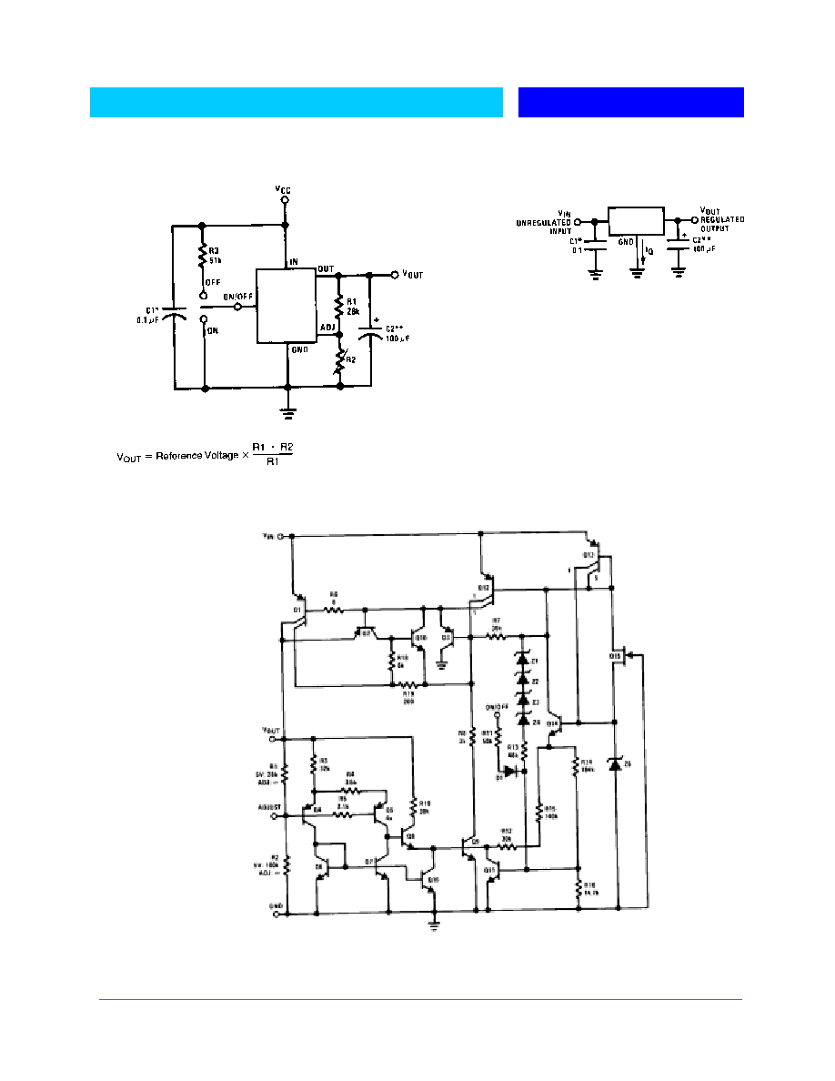
TYPICAL APPLICATIONS
LM2931 ADJUSTABLE OUTPUT
LM2931
ADJ.
LM2931 ADJUSTABLE OUTPUT
LM2931
ADJ.
LM2931
LM2931 Fixed Output
LM2931
LM2931 Fixed Output
SCHEMATIC DIAGRAM
Document Outline