 | –≠–ª–µ–∫—Ç—Ä–æ–Ω–Ω—ã–π –∫–æ–º–ø–æ–Ω–µ–Ω—Ç: LM2941 | –°–∫–∞—á–∞—Ç—å:  PDF PDF  ZIP ZIP |
Bay Linear, Inc
2478 Armstrong Street, Livermore, CA 94550 Tel: (925) 989-7144, Fax: (925) 940-9556 www.baylinear.com
1.25A High Current Low Dropout
LM2940/2941
Voltage Regulator Adjustable
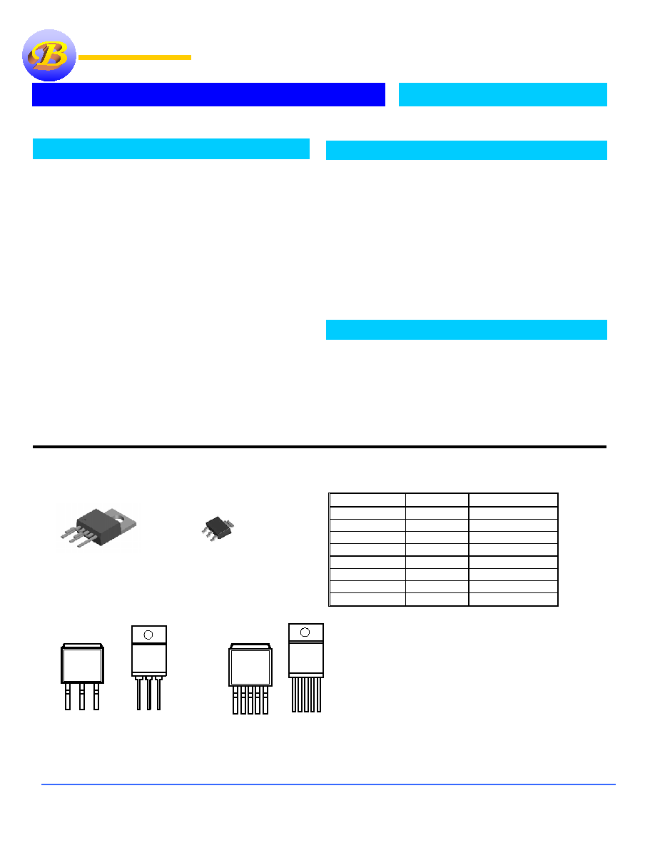
Pin Connection
Ordering Information
Devices Package Temp.
LM2940T TO-220-3
-40
∞C to 125 ∞C
LM2941T TO-220-5
-40
∞C to 125 ∞C
LM2940S TO-263-3
-40
∞C to 125 ∞C
LM2941S TO-263-5
-40
∞C to 125 ∞C
LM2940N SOT-223-3
-40
∞C to 125 ∞C
LM2941N SOT-223-5
-40
∞C to 125 ∞C
LM2940J LPDD-3
-40
∞C to 125 ∞C
LM2941J LPDD-5
-40
∞C to 125 ∞C
Description
The Bay Linear LM2940 & LM2941 is a 1.25A high accuracy, low
dropout voltage regulator with only 40mV at light loads and
350mV(Typ.)@ 1.0A) and low quiescent current of 240
µA typical.
The LM2940/41 is designed for low voltage a application that
requires lower dropout voltage and faster transient response. This
device is an excellent choice for use in powering low voltage
applications where require a lower dropout, faster transient response
to regulate from +2.5V to 3.8V supplies and as a post regulator for
switching supplies applications.
The LM2940/41 offers full protection against over-current faults,
reversed input polarity, reversed load insertion, and positive and
negative transient voltage. On-Chip trimming adjusts the reference
voltage to 1%. The LM2940-xx devices are in 3 pin fixed voltage
regulators. The LM2941 include an Enable pin in the 5 pin
packages
.
The LM2940/41 are offered in a 3 & 5-pin SOT-223, TO-220 &
TO-263 package compatible with other 3 terminal regulators. The
LM2940/41 is also offer in a new LPDD (Low Profile TO-263)
package from 4.47 mm (DD) tickness down to only 1.27 mm
(LPDD) t t l ti k
Features
∑ High output accuracy of 1%
∑ Output Adjustable from 1.24V to 26V
∑ Output Current of 1.25A
∑ Low Dropout Voltage
∑ Low quiescent current
∑ Extremely Tight Load & Line Regulation
∑ Reverse-battery and "Load Dump" Protection
∑ Zero Current Shutdown Mode (5-pin version)
∑ Offer in TO-263, TO-220, SOT-223, & New Slim
LPDD
∑
Similar to industry Standard MIC2940LM2941
Applications
∑ Powering VGA & Sound Card
∑ LCD Monitor
∑ Battery Powered Equipments/Laptop & Notebook
∑ SMPS Post Regulator / DC to DC Modules
∑ High Efficiency Linear Power Supply
∑ Adjustable Power Supply
∑
Bar Code Scanners
Bay Linear
Inspire the Linear Power
TO-263-3 Package
V
OUT
GND
V
IN
BAY
B2940
Front View
1
2
3
Front View
TO-220-3 Package
BAY
B2940
V
IN
V
OUT
GND
TO-263-5 Package
Top View
4 5
BAY
B2941
3
2
1
GND
OUPUT
1)
3)
4)
5)
2) ON/OFF
ADJUST
INPUT
TO-220-5 Package
Top View
BAY
B2941
1 2 3 4 5
TO-263-3 Package
V
OUT
GND
V
IN
BAY
B2940
Front View
1
2
3
Front View
TO-220-3 Package
BAY
B2940
V
IN
V
OUT
GND
TO-263-3 Package
V
OUT
GND
V
IN
BAY
B2940
Front View
1
2
3
Front View
TO-220-3 Package
BAY
B2940
V
IN
V
OUT
GND
Front View
TO-220-3 Package
BAY
B2940
V
IN
V
OUT
GND
TO-263-5 Package
Top View
4 5
BAY
B2941
3
2
1
GND
OUPUT
1)
3)
4)
5)
2) ON/OFF
ADJUST
INPUT
TO-220-5 Package
Top View
BAY
B2941
1 2 3 4 5
TO-263-5 Package
Top View
4 5
BAY
B2941
3
2
1
GND
OUPUT
1)
3)
4)
5)
2) ON/OFF
ADJUST
INPUT
GND
OUPUT
1)
3)
4)
5)
2) ON/OFF
ADJUST
INPUT
TO-220-5 Package
Top View
BAY
B2941
1 2 3 4 5
TO-220-5 Package
Top View
BAY
B2941
1 2 3 4 5
Bay Linear, Inc
2478 Armstrong Street, Livermore, CA 94550 Tel: (925) 989-7144, Fax: (925) 940-9556 www.baylinear.com
LM2940/41
ABSOLUTE MAXIMUM RATINGS
Lead Temp. (Soldering, 5 Seconds).................................260∞C
Input Voltage ........................................................26V
Storage Temperature Range.............................. -65∞ to +150∞C
Maximum Output Current....................................3.5A
Operating Junction Temperature Range
Input Supply Voltage (Note1) (Survival)-20V to +60V
LM2940/2941
Control
Section.................. -45∞C +125∞C
LM2940/2941 Power Transistor.................-45∞C +150∞C
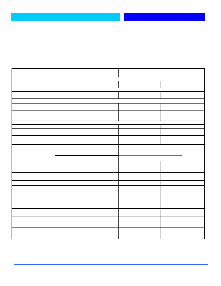
ELECTRICAL CHARACTERISTICS
(NOTE 1) at I
OUT
= 5mA, V
IN
=V
OUT
+ 1V, I
l
= 1000mA, C
L
= 10
µF. Ta=25∞C, unless otherwise
specified. The LM2941 is programmed to output 5V and has V
SHUTDOWN
0.6V
PARAMETER
CONDITIONS Typ
LM2940
Min Max
Units
2.5V Version
Output Voltage (Note 2)
I
OUT
= 5mA
5mA
I
OUT
1.25A, 4.75VV
IN
26V
2.5
2.5
2.475
2.450
2.525
2.550
V
3.3V Version2.
Output Voltage (Note 2)
I
OUT
= 5mA
5mA
I
OUT
1.25A, 4.75VV
IN
26V
3.3
3.3
3.267
3.234
3.330
3.366
V
5.0V Version
Output Voltage (Note 2)
I
OUT
= 5mA
5mA
I
OUT
1.25A, 5.5VV
IN
26V
5.0
5.0
4.95
4.90
5.05
5.10
V
Output Voltage
Accuracy
5mA
I
OUT
1.0 A
-1
-2
-2.5
1
2
2.5
%
All Voltage Options
Line Regulation
I
O
= 5mA, (V
OUT
+ 1V)
V
IN
26V
0.06
0.5 %
Load Regulation
V
IN
= V
OUT
+ 5V, 5mA
I
OUT
1 A
(Note 2, 6)
0.2 1.6 %
V∞
20
100
ppm/
∞C
T
Output Voltage (Note 6)
Temperature Coef.
I
O
= 5mA
80 150
I
O
= 1000mA
350 450
Dropout Voltage
I
O
= 1.25A
400 600
mV
Ground Current
I
O
= 5mA, V
IN
= V
OUT
, +1V
I
O
= 1000mA, V
IN
= V
OUT
, +1V
I
O
= 1.25A
240
22
35
350
35
70
µA
mA
I
GNDDO
Ground Pin Current at
Dropout
V
IN
= 0.5V less than specified V
OUT
I
OUT
= 10mA
0.9
mA
Current Limit
V
OUT
= 0V (Note 4)
1.7
1.5
A
Output Noise Voltage
(10Hz to 100kHz)
I
L
= 100mA
C
L
= 10
µF
C
L
= 33
µF
400
260
µV
RMS
Reference Voltage
1.235
1.223
1.210
1.247
1.260
V
V
max
Reference Voltage
(Note 8)`
1.204 1.266 V
Adjust Pin
Bias Current
40 80
120
nA
Reference Voltage
Temperature
Coefficient
(Note 7)
20
ppm/
∞C
Adjust Pin Bias
Current Temperature
Coefficient
0.1
nA/
∞C
Bay Linear, Inc
2478 Armstrong Street, Livermore, CA 94550 Tel: (925) 989-7144, Fax: (925) 940-9556 www.baylinear.com
LM2940/2941
ENABLE Input LM2941
Input Logic Voltage
Low (OFF)
High (ON)
2.4
0.8
V
V
EN
= 26V
100
600
750
V
Enable Pin
Input Current
V
EN
= 0.8V
2.5
5
µA
Regulator Output
Current in Shutdown
(Note 10)
10
500
µA
NOTES:
The Bold specifications apply to the full operating temperature range.
Note 1: Maximum positive supply voltage of 60V must be of limited duration (<100msec) and duty cycle.) The maximum continuous supply voltage is 26V.
Note 2: Full load current (I
FL
) is defined as 1.25A for the LM2941.
Note 3: Dropout voltage is defined as the input-to output differential when the output voltage drops to 99% of its nominal value with V
OUT
+ 1V applied to V
IN
.
Note 4: VIN = V
OUT
(NOMINAL)
+1V. For example, use V
IN
= 4.3V for a 3.3V regulator. Employ pulse-testing procedures to minimize temperature rise.
Note 5: Ground pin current is the regulator quiescent current. The total current drawn from the source is the sum of the load current to the ground current.
Note 6: Output voltage temperature coefficient is defined as the worst case voltage changed divided by the total temperature range.
Note 7: Thermal regulation is defined as the change in the output voltage at a time T after a change in power dissipation is applied, excluding load or line regulation
effects. Specifications are for a 200mA load pulse as V
IN
= 20V (a 4W pulse) for T = 10ms.
Note 8: VREF
V
OUT
(V
IN
- 1), 2.3V
V
IN
26V, 10mA < I
L
I
FL
, T
J
T
JMAX
Note 9: Comparator threshold is expressed in terms of a voltage differential at the Adjust terminal below the nominal reference voltage measured 6V input. To express
these thresholds in terms of output voltage change, multiply the error amplifier gain = V
OUT
/V
REF
= (R1 + R2)/R2. For example, at a programmable output voltage of
5V, the Error output is guaranteed to go low when the output drops by 95mVx 5V/ 1.240V = 38mV. Threshold remains constant as a percent of V
OUT
as V
OUT
is varied,
with the dropout warning occurring at typically 5% below nominal, 7.7% guaranteed.
Note 10: V
EN
0.8V and V
IN
26V, V
OUT
= 0.
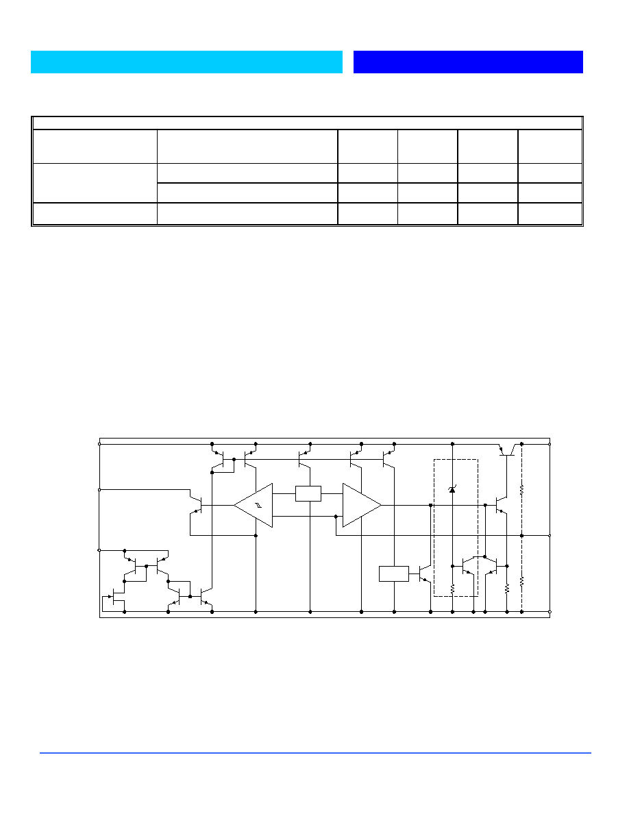
BLOCK DIAGRAM
Reference
Thermal
Shutdown
EN
IN
OUT
ADJ
GND
O.V
I
LIMIT
28V
R1*
R2*
1.180V
1.240V
+
+
-
-
FLAG
Bay Linear, Inc
2478 Armstrong Street, Livermore, CA 94550 Tel: (925) 989-7144, Fax: (925) 940-9556 www.baylinear.com
LM2940/2941
APPLICATION HINTS
The Bay Linear LM2941 incorporates protection against over-current
faults, reversed load insertion, over temperature operation, and
positive and negative transient voltage. However, the use of an output
capacitor is required in order to insure the stability and the
performances.
Thermal Consideration
Although the LM2941 offers limiting circuitry for overload
conditions, it is necessary not to exceed the maximum junction
temperature, and therefore to be careful about thermal resistance. The
heat flow will follow the lowest resistance path, which is the Junction-
to-case thermal resistance. In order to insure the best thermal flow of
the component, a proper mounting is required. Note that the case of
the device is electrically connected to the output. The
case has to be electrically isolated, a thermally conductive spacer can
be used. However do not forget to consider its contribution to thermal
resistance.
Assuming:
V
IN
= 10V, V
OUT
= 5V, I
OUT
= 1.5A, T
A
= 90
∞C,
CASE
= 1
∞C/W (no
external heat sink, no wind)
Power dissipation under these conditions
P
D
= (V
IN
≠ V
OUT
) * I
OUT
= 7.5W
Junction Temperature
T
J
= T
A
+ P
D
* (
CASE
+
JC
)
For the Control Section
T
J
= 90
∞C + 7.5W*(1∞C/W + 0.6∞C/W) = 102∞C
114
∞C < T
JUNCTION MAX
for the control section.
For the Power Section
T
J
= 90
∞C + 7.5W*(1∞C/W + 1.6∞C/W) = 104.5∞C
109.5
∞C < T
JUNCTION MAX
for the power transistor.
In both case reliable operation is insured by adequate junction
temperature.
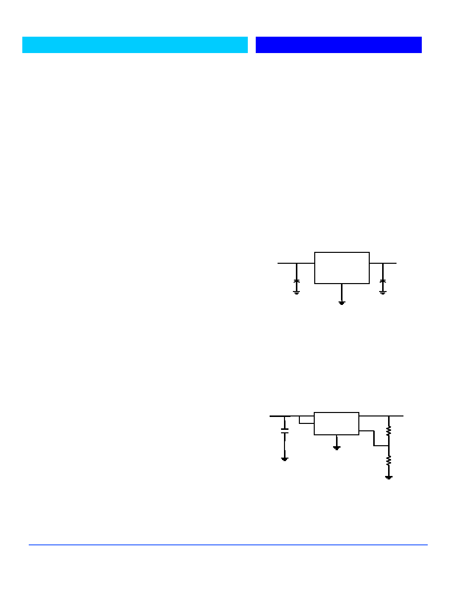
Capacitor Requirements
The output capacitor is needed for stability and to minimize the output
noise. The required value of the capacitor varies with the load.
However, a minimum value of 10
µF Aluminum will guarantee
stability over load. A tantalum capacitor is recommended for a fast
load transient response.
If the power source has high AC impedance, a 0.1
µF capacitor
between input & ground is recommended. This capacitor should have
good characteristics up to 250 kHz.
Minimum Load Current
To ensure a proper behavior of the regulator at light load, a
minimum load of 5mA for LM2941 is required.
Adjustable Regulator Design
B29152/53 are adjustable regulators and maybe programmed for
any value between 1.25V and 26V using two resistors. The relation
between the resistors is given by:
R
1
=R
2
(V
OUT
/1.240 ≠1)
Resistors have a large value up to 1m
in order to reduce the
current consumption. This might be interesting in the case of
widely varying load currents.
Enable Input
LM2941 features enable input allowing turning ON & OFF the
device. EN has been designed to be compatible with TTL/CMOS
logic. When the regulator is ON, the current flowing through this
pin is approximately 20
µA.
4
5
3
2
1
BAY
B2941
V
OUT
V
IN
R
1
R
2
Fig. 2 Adjustable Output Voltage Regulator
V
OUT
= V
REF
X [1 + (R
1
/
R
2
)]
For best results, the total series resistance should be small
enough to pass the minimum regulator load current
4
5
3
2
1
BAY
B2941
V
OUT
V
IN
R
1
R
2
Fig. 2 Adjustable Output Voltage Regulator
V
OUT
= V
REF
X [1 + (R
1
/
R
2
)]
For best results, the total series resistance should be small
enough to pass the minimum regulator load current
BAY
B2940
Fig.1 Basic Fixed Output Regulator
V
OU
T
V
IN
BAY
B2940
Fig.1 Basic Fixed Output Regulator
V
OU
T
V
IN

Bay Linear, Inc
2478 Armstrong Street, Livermore, CA 94550 Tel: (925) 989-7144, Fax: (925) 940-9556 www.baylinear.com
LM2940/2941
Advance Information- These data sheets contain descriptions of products that are in development. The specifications are based on the engineering calculations, computer simulations and/
or initial prototype evaluation.
Preliminary Information- These data sheets contain minimum and maximum specifications that are based on the initial device characterizations. These limits are subject to change upon the
completion of the full characterization over the specified temperature and supply voltage ranges.
The application circuit examples are only to explain the representative applications of the devices and are not intended to guarantee any circuit design or permit any
industrial property right to other rights to execute. Bay Linear takes no responsibility for any problems related to any industrial property right resulting from the use of
the contents shown in the data book. Typical parameters can and do vary in different applications. Customer's technical experts must validate all operating parameters
including " Typical" for each customer application.
LIFE SUPPORT AND NUCLEAR POLICY
Bay Linear products are not authorized for and should not be used within life support systems which are intended for surgical implants into the body
to support or sustain life, in aircraft, space equipment, submarine, or nuclear facility applications without the specific written consent of Bay Linear
President.