LS E675
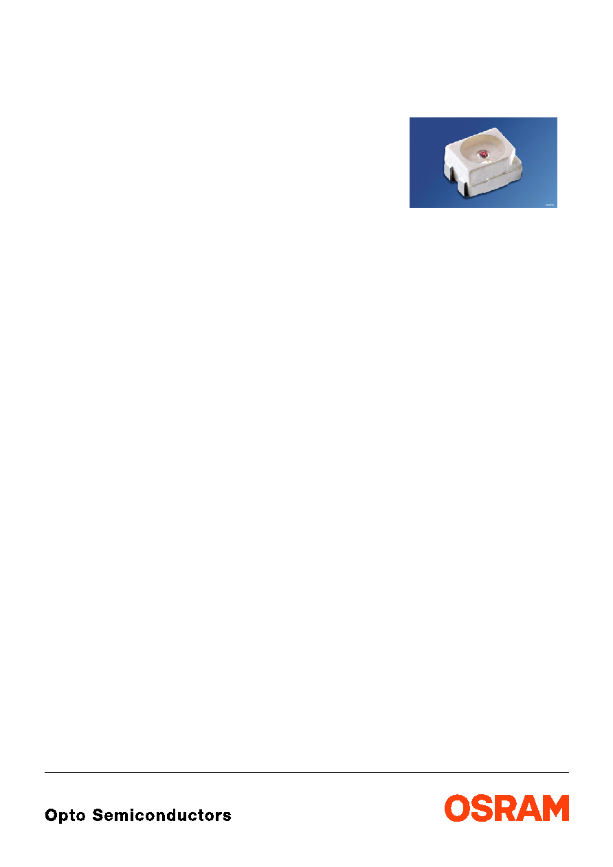
Power TOPLED
Æ
Hyper-Bright LED
2001-01-25
1
Besondere Merkmale
∑ Geh‰usetyp: weiþes P-LCC-4 Geh‰use
∑ Besonderheit des Bauteils: mehr Licht durch
erhˆhten optischen Wirkungsgrad; hˆhere
Umgebungstemperatur bei gleichem Strom im
Vergleich zur TOPLED mˆglich
∑ Wellenl‰nge: 632 nm (super-rot)
∑ Abstrahlwinkel: Lambertscher Strahler (120∞)
∑ Technologie: InGaAlP
∑ optischer Wirkungsgrad: 12 lm/W
∑ Gruppierungsparameter: Lichtst‰rke
∑ Verarbeitungsmethode: f¸r alle
SMT-Best¸cktechniken geeignet
∑ Lˆtmethode: IR Reflow Lˆten und
Wellenlˆten (TTW)
∑ Vorbehandlung: nach JEDEC Level 2
∑ Gurtung: 8 mm Gurt mit 2000/Rolle, ¯180 mm
oder 8000/Rolle, ¯330 mm
∑ ESD-Festigkeit: ESD-sicher bis 2 kV nach
EOS/ESD-5.1-1993
Anwendungen
∑ Ampelanwendung
∑ Hinterleuchtung (LCD, Schalter, Tasten,
Displays, Werbebeleuchtung)
∑ Innen- und Auþenbeleuchtung im Auto-
mobilbereich (z.B. Instrumentenbeleuchtung
und Bremslichter)
∑ Ersatz von Kleinst-Gl¸hlampen
∑ Markierungsbeleuchtung (z.B. Stufen,
Fluchtwege, u.‰.)
∑ Signal- und Symbolleuchten
Features
∑ package: white P-LCC-4 package
∑ feature of the device: more light due to higher
optical efficiency; higher ambient temperature
at the same current possible compared to
TOPLED
∑ wavelength: 632 nm (super-red)
∑ viewing angle: Lambertian Emitter (120∞)
∑ technology: InGaAlP
∑ optical efficiency: 12 lm/W
∑ grouping parameter: luminous intensity
∑ assembly methods: suitable for all
SMT assembly methods
∑ soldering methods: IR reflow soldering and
TTW soldering
∑ preconditioning: acc. to JEDEC Level 2
∑ taping: 8 mm tape with 2000/reel, ¯180 mm or
8000/reel, ¯330 mm
∑ ESD-withstand voltage: up to 2 kV acc. to
EOS/ESD-5.1-1993
Applications
∑ traffic lights
∑ backlighting (LCD, switches, keys, displays,
illuminated advertising)
∑ interior and exterior automotive lighting
(e.g. dashboard backlighting and brake lights)
∑ substitution of micro incandescent lamps
∑ marker lights (e.g. steps, exit ways, etc.)
∑ signal and symbol luminaire
2001-01-25
2
LS E675
Helligkeitswerte werden mit einer Stromeinpr‰gedauer von 25 ms und einer Genauigkeit von ±11 %
ermittelt.
Luminous intensity is tested at a current pulse duration of 25 ms and an accuracy of ±11 %.
-1 gesamter Farbbereich (siehe Seite 5)
-1 Total color tolerance range (see page 5)
Typ
Type
Emissions-
farbe
Color of
Emission
Farbe der
Lichtaustritts-
fl‰che
Color of the
Light Emitting
Area
Lichtst‰rke
Luminous
Intensity
I
F
= 50 mA
I
V
(mcd)
Lichtstrom
Luminous
Flux
I
F
= 50 mA
V
(mlm)
Bestellnummer
Ordering Code
LS E675-S1T1-1
LS E675-T1U2-1
amber
colorless clear
180 ...355
280 ...710
770 (typ.)
1400 (typ.)
Q62703-Q6103
Q62703-Q6104
Helligkeits-Gruppierungsschema
Luminous Intensity Groups
Lichtgruppe
Luminous Intensity Group
Lichtst‰rke
Luminous Intensity
I
V
(mcd)
Lichtstrom
Luminous Flux
V
(mlm)
S1
S2
T1
T2
U1
U2
180 ... 224
224 ... 280
280 ... 355
355 ... 450
450 ... 560
560 ... 710
600 (typ.)
760 (typ.)
950 (typ.)
1200 (typ.)
1500 (typ.)
1900 (typ.)

LS E675
2001-01-25
3
Grenzwerte
Maximum Ratings
Bezeichnung
Parameter
Symbol
Symbol
Wert
Value
Einheit
Unit
Betriebstemperatur
Operating temperature range
T
op
≠ 40 ... + 100
∞C
Lagertemperatur
Storage temperature range
T
stg
≠ 40 ... + 100
∞C
Sperrschichttemperatur
Junction temperature
T
j
+ 125
∞C
Durchlassstrom
Forward current
I
F
70
mA
Stoþstrom
Surge current
t
10
µ
s, D = 0.1
I
FM
0.1 A
Sperrspannung
Reverse voltage
V
R
5
V
Leistungsaufnahme
Power consumption
T
A
25 ∞C
P
tot
180
mW
W‰rmewiderstand
Thermal resistance
Sperrschicht/Umgebung
Junction/ambient
Sperrschicht/Lˆtpad
Junction/soldering point
Montage auf PC-Board FR 4 (Padgrˆþe
16 mm
2
)
mounted on PC board FR 4 (pad size
16 mm
2
)
R
th JA
R
th JS
300
130
K/W
K/W
2001-01-25
4
LS E675
Kennwerte (
T
A
= 25 ∞C)
Characteristics
Bezeichnung
Parameter
Symbol
Symbol
Wert
Value
Einheit
Unit
Wellenl‰nge des emittierten Lichtes
(typ.)
Wavelength at peak emission
I
F
= 50 mA
peak
645
nm
Dominantwellenl‰nge
1)
(typ.)
Dominant wavelength
1)
I
F
= 50 mA
dom
632
± 6
nm
Spektrale Bandbreite bei 50 %
I
rel max
(typ.)
Spectral bandwidth at 50 %
I
rel max
I
F
= 50 mA
18
nm
Abstrahlwinkel bei 50 %
I
V
(Vollwinkel)
(typ.)
Viewing angle at 50 %
I
V
2
120
Grad
deg.
Durchlassspannung
2)
(typ.)
Forward voltage
2)
(max.)
I
F
= 50 mA
V
F
V
F
2.1
2.5
V
V
Sperrstrom
(typ.)
Reverse current
(max.)
V
R
= 5 V
I
R
I
R
0.01
10
µ
A
µ
A
Temperaturkoeffizient von
peak
(typ.)
Temperature coefficient of
peak
I
F
= 50 mA;
TC
peak
0.15
nm/K
Temperaturkoeffizient von
dom
(typ.)
Temperature coefficient of
dom
I
F
= 50 mA;
TC
dom
0.04
nm/K
Temperaturkoeffizient von
V
F
(typ.)
Temperature coefficient of
V
F
I
F
= 50 mA;
TC
V
≠ 3.4
mV/K
Optischer Wirkungsgrad
(typ.)
Optical efficiency
I
F
= 50 mA
opt
12
lm/W
10
∞
C
≠
T
100
∞
C
10
∞
C
≠
T
100
∞
C
10
∞
C
≠
T
100
∞
C
LS E675
2001-01-25
5
1)
Wellenl‰ngen werden mit einer
Stromeinpr‰gedauer von 25 ms und einer
Genauigkeit von ±1 nm ermittelt.
Wavelengths are tested at a current pulse
duration of 25 ms and an accuracy of ±1 nm.
2)
Spannungswerte werden mit einer
Stromeinpr‰gedauer von 1 ms und einer
Genauigkeit von ±0.05 V ermittelt.
Voltages are tested at a current pulse duration
of 1 ms and an accuracy of ±0.05 V.
Gruppenbezeichnung auf Etikett
Group Name on Label
Beispiel: T1-1
Example: T1-1
Lichtgruppe
Luminous Intensity Group
Halbgruppe
Half Group
Wellenl‰nge
Wavelength
T
1
1
2001-01-25
6
LS E675
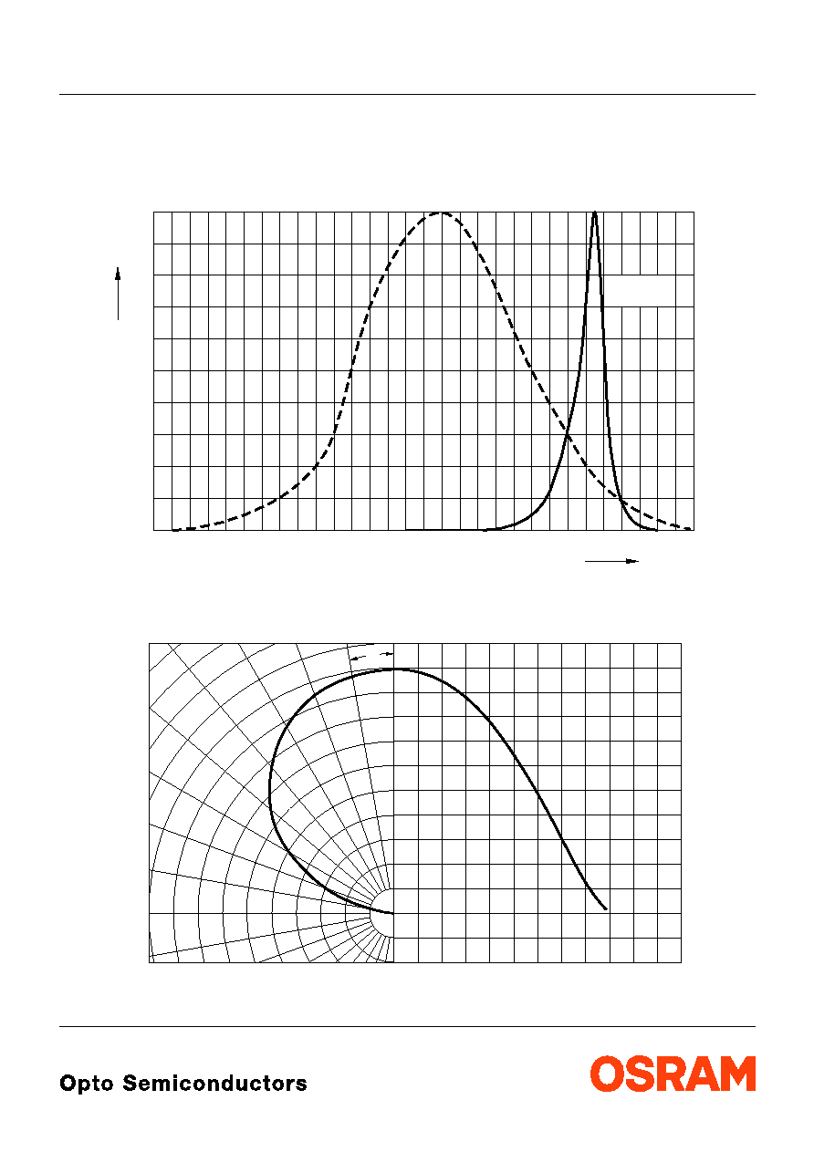
Relative spektrale Emission
I
rel
=
f
(
),
T
A
= 25 ∞C,
I
F
= 50 mA
Relative Spectral Emission
V(
) = spektrale Augenempfindlichkeit
Standard eye response curve
Abstrahlcharakteristik
I
rel
=
f
(
)
Radiation Characteristic
OHL01486
400
0
20
40
60
80
100
450
500
550
600
650
700
nm
%
I
rel
V
super-red
0
0.2
0.4
1.0
0.8
0.6
1.0
0.8
0.6
0.4
0∞
10∞
20∞
40∞
30∞
OHL01660
50∞
60∞
70∞
80∞
90∞
100∞
0∞
20∞
40∞
60∞
80∞
100∞
120∞
LS E675
2001-01-25
7
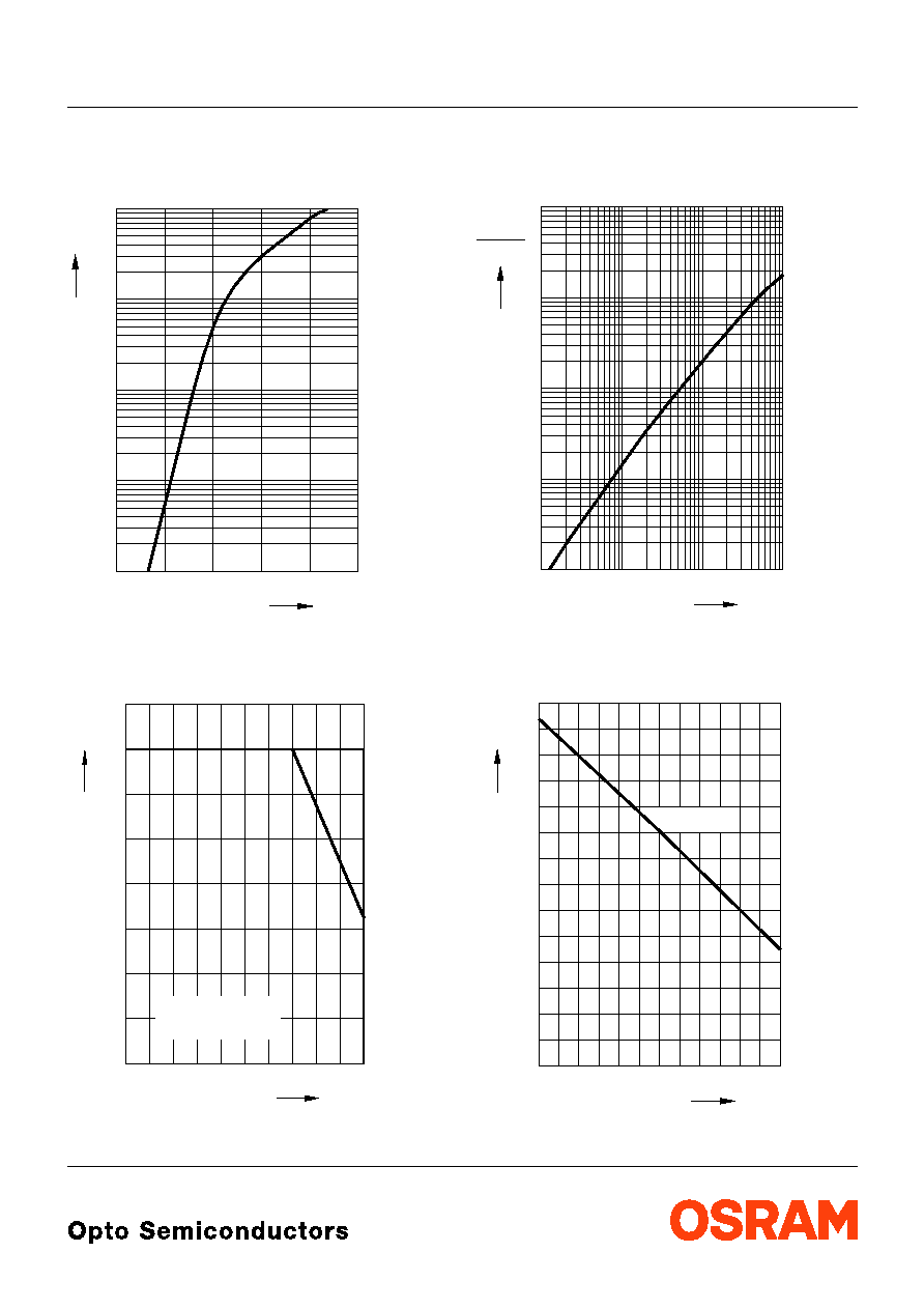
Durchlassstrom
I
F
=
f
(
V
F
)
Forward Current
T
A
= 25 ∞C
Maximal zul‰ssiger Durchlassstrom
I
F
=
f
(
T
)
Max. Permissible Forward Current
Relative Lichtst‰rke
I
V
/
I
V(50 mA)
=
f
(
I
F
)
Relative Luminous Intensity
T
A
= 25 ∞C
Relative Lichtst‰rke
I
V
/
I
V(25 ∞C)
=
f
(
T
A
)
Relative Luminous Intensity
I
F
= 50 mA
OHL00444
1.4
mA
10
1
10
5
-2
5
0
10
-1
5
10
V
10
2
F
I
F
V
1.6
1.8
2.0
2.2
2.4
OHL01413
0
0
20
40
60
80 ∞C 100
T
I
F
20
40
60
80
mA
A
T
S
T
temp. ambient
temp. solder point
A
S
10
30
70
50
I
OHL00437
F
-1
10
V (50 mA)
I
10
-3
-2
-1
0
1
10
10
10
10
10
0
10
1
10
2
5
5
5
5
5
mA
I
V
OHL01638
-20
super-red
0
V
I
A
T
0.2
0.4
0.6
0.8
1.0
1.2
mcd
1.4
0
20
40
60
∞C 100
LS E675
2001-01-25
8
Zul‰ssige Impulsbelastbarkeit
I
F
=
f
(
t
p
)
Permissible Pulse Handling Capability
Duty cycle
D
= parameter,
T
A
= 25 ∞C
Zul‰ssige Impulsbelastbarkeit
I
F
=
f
(
t
p
)
Permissible Pulse Handling Capability
Duty cycle
D
= parameter,
T
A
= 85 ∞C
OHL01505
F
I
0
0.02
0.04
0.06
0.08
0.1
0.12
A
p
t
-5
10
-4
10
-3
10
-2
10
-1
10
0
10
1
10
2
10
0.005
0.05
0.5
s
OHL01506
F
I
0
0.02
0.04
0.06
0.08
0.10
0.12
A
p
t
-5
10
-4
10
-3
10
-2
10
-1
10
0
10
1
10
2
10
0.005
0.05
0.5
s

LS E675
2001-01-25
9
Maþzeichnung
Package Outlines
Maþe werden wie folgt angegeben: mm (inch) / Dimensions are specified as follows: mm (inch).
marking
Package
4
∞
±1
GPLY6991
A
C
C
C
0.8 (0.031)
0.6 (0.024)
2.6 (0.102)
2.1 (0.083)
2.3 (0.091)
3.0 (0.118)
3.4 (0.134)
3.0 (0.118)
(2.4 (0.094))
0.5 (0.020)
1.1 (0.043)
3.7 (0.146)
3.3 (0.130)
0.12 (0.005)
0.18 (0.007)
0.1 (0.004) typ
0.4 (0.016)
0.6 (0.024)
0.9 (0.035)
0.7 (0.028)
2.1 (0.083)
1.7 (0.067)
2001-01-25
10
LS E675
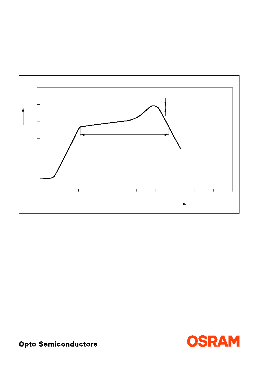
Lˆtbedingungen
Vorbehandlung nach JEDEC Level 2
Soldering Conditions Preconditioning acc. to JEDEC Level 2
IR-Reflow Lˆtprofil
(nach IPC 9501)
IR Reflow Soldering Profile
(acc. to IPC 9501)
OHLY0597
0
0
50
100
150
200
250
50
100
150
200
250
300
T
t
∞C
s
240-245 ∞C
10-40 s
183 ∞C
120 to 180 s
Defined for Preconditioning: up to 6 K/s
Ramp-down rate up to 6 K/s
Ramp-up rate up to 6 K/s
Defined for Preconditioning: 2-3 K/s
LS E675
2001-01-25
11
Wellenlˆten (TTW)
(nach CECC 00802)
TTW Soldering
(acc. to CECC 00802)
OHLY0598
0
0
50
100
150
200
250
50
100
150
200
250
300
T
t
C
s
235 C
10 s
C
... 260
1. Welle
1. wave
2. Welle
2. wave
5 K/s
2 K/s
ca 200 K/s
C
C
... 130
100
2 K/s
Zwangsk¸hlung
forced cooling
Normalkurve
standard curve
Grenzkurven
limit curves
2001-01-25
12
LS E675
Empfohlenes Lˆtpaddesign
IR Reflow Lˆten
Recommended Solder Pad
IR Reflow Soldering
Maþe werden wie folgt angegeben: mm (inch) / Dimensions are specified as follows: mm (inch).
OHLPY439
Padgeometrie f¸r
verbesserte W‰rmeableitung
improved heat dissipation
Paddesign for
Lˆtstoplack
Solder resist
1.1 (0.043)
4.5 (0.177)
1.5 (0.059)
2.6 (0.102)
3.3 (0.130)
0.5 (0.020)
7.5 (0.295)
0.4 (0.016)
Cathode marking
Kathoden Markierung /
Cu Fl‰che / 12 mm per pad
2
Cu-area
_
<
3.3 (0.130)
LS E675
2001-01-25
13
Empfohlenes Lˆtpaddesign
Wellenlˆten (TTW)
Recommended Solder Pad
TTW Soldering
Maþe werden wie folgt angegeben: mm (inch) / Dimensions are specified as follows: mm (inch).
Gurtung / Polarit‰t und Lage
Verpackungseinheit 2000/Rolle, ¯180 mm
oder 8000/Rolle, ¯330 mm
Method of Taping / Polarity and Orientation Packing unit 2000/reel, ¯180 mm
or 8000/reel, ¯330 mm
Maþe werden wie folgt angegeben: mm (inch) / Dimensions are specified as follows: mm (inch).
OHAY0583
6.1 (0.240)
2.8 (0.110)
2 (0.079)
3 (0.118)
6 (0.236)
3.5 (0.138)
1.5 (0.059)
2 (0.079)
3.5 (0.138)
1 (0.039)
8 (0.315)
2.8 (0.110)
0.5 (0.020)
7.5 (0.295)
Solder resist
Lˆtstoplack
PCB-direction
Bewegungsrichtung
der Platine
2 (0.079)
Padgeometrie f¸r
improved heat dissipation
verbesserte W‰rmeableitung
Paddesign for
2
Cu Fl‰che / > 12 mm per pad
Cu-area
OHAY0536
C
C
C
A
4 (0.157)
2.9 (0.114)
1.5 (0.059)
4 (0.157)
3.6 (0.142)
3.5 (0.138)
2 (0.079)
1.75 (0.069)
8 (0.315)