 | –≠–ª–µ–∫—Ç—Ä–æ–Ω–Ω—ã–π –∫–æ–º–ø–æ–Ω–µ–Ω—Ç: N1153 | –°–∫–∞—á–∞—Ç—å:  PDF PDF  ZIP ZIP |
1
5 Bit Programmable Synchronous
DC/DC Controller
NIKO-SEM
N1153
AUG-03-2001
GENERAL DESCRIPTION
The N1153 is a low-cost, 5 bit TTL-compatible
input, digital-to-analog (DAC) programmable,
synchronous buck converter controller design-
ed specifically to power the Pentium
Æ
II as well
as the next generation of P6 family or other
high performance core logic in desktop person-
al computer CPU applications.
Additional features also include temperature
compensated voltage reference, triangle wave
oscillator, current limits comparator, frequency
shift over-current protection, and an access-
ible, internally compensated error amplifier,
power good signal, logic compatible shutdown,
and over voltage protection are also provide.
The N1153 operates at a fixed 200KHz, provid-
ing an optimum compromise between efficien-
cy, external component size, and cost.
FEATURES
High performance and low cost solution
Synchronous operation with high efficiency
TTL-compatible 5 bit DAC, output voltage
selection from 1.3V to 3.5V programmable
High current totem pole output, up to 2 A
for direct driving of the external N-Channel
power MOSFETs.
200 KHz fixed frequency internal oscillator
Fast transient response
Power-Good output voltage monitor
Over-Voltage and Over-Current protection
APPLICATIONS
Powering Pentium
Æ
II, III or Deschutes,
K6 and other advanced processor
Multiple microprocessor supplies
High power DC to DC controller
Programmable power supplies
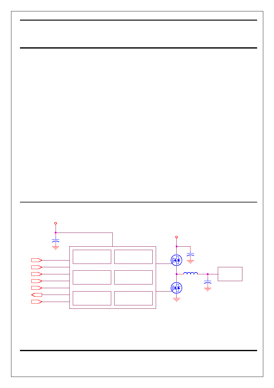
TYPICAL APPLICATION
5V
12V
+
+
+
VID 0
VID 4
VID 1
VID 2
VID 3
P.G
S.D
VCORE
D/A AND
SHUT-DOWN
LOGIC
TEMP. COMPENSATED
VOLTAGE REFERENCE
TRIANGLE
WAVE
OSCILLATOR
CURRENT
LIMIT
COMPARATOR
FREQUENCY SHIFT
OVER-CURRENT
PROTECTION
INTERNALLY
COMPENSATED
ERROR AMPLIFIER
N1153, Motherboard Power Regulation for Computers
2
5 Bit Programmable Synchronous
DC/DC Controller
NIKO-SEM
N1153
AUG-03-2001
ABSOLUTE MAXIMUM RATINGS
V
CC
to GND, V
IN
- 0.3V to 7V
Operating Temperature
Range, T
A
0 to 70 ∞C
BST to GND
-0.3V to 15V
Operating Junction
Temperature Range, T
J
0 to 125 ∞C
Thermal Resistance
Junction to Case,
JC
30 ∞C/W
Storage Temperature
Range, T
STG
-65 to 150 ∞C
Thermal Resistance
Junction to Ambient,
JA
90 ∞C/W
Lead Temperature, T
LEAD
(Soldering, 10 Seconds)
300 ∞C
ELECTRICAL SPECIFICATIONS
<Unless specified: V
CC
= 4.75V ~ 5.25V, GND = PGND = 0V, VOSENSE = V
O
, 0mV < (CS
+
- CS
-
) < 60mV, T
A
= 25
∞
C>
PARAMETER
CONDITIONS
MIN TYP MAX UNITS
Supply Voltage
V
CC
4.2
7
V
Supply Current
V
CC
= 5.0V
5
mA
Output Voltage
I
O
= 2A
See Table 1.
Load Regulation
I
O
= 0.3A to 15A
1
%
Line Regulation
All VID Codes
0.5
%
Gain (A
OL
) V
OSENSE
to V
O
35
dB
Current Limit Voltage
60
70
80
mV
Oscillator Frequency
180 200 220
KHz
Oscillator Max Duty Cycle
90
95
%
Peak DH Sink/Source Current
BSTH - DH = 4.5V, DH - PGNDH = 2V
1 A
Peak DL Sink/Source Current
BSTL - DL = 4.5V, DL - PGNDL = 2V
1 A
OVP Threshold Voltage
120
%
OVP Source Current
V
OVP
= 3.0V
10
mA
Power-Good Threshold Voltage
85
115
%
Dead Time
100 200
nS

3
5 Bit Programmable Synchronous
DC/DC Controller
NIKO-SEM
N1153
AUG-03-2001
PIN CONFIGURATIONS
PIN DEFINITIONS
Pin #
Pin Name
Pin Function Description
1
GND
Small signal analog and digital ground
2 V
CC
Input
voltage
3
OVP
High signal out if V
O
>set point +20%
4 PWRGOOD
*
Open collector logic output, high if V
O
within 10% of set point
5
CS-
Current sense input (Negative)
6
CS+
Current sense input (Positive)
7
PGNDL
Power ground for high side switch
8
DH
High side driver output
9 NC
No
connected
10
PGNDL
Power ground for high side switch
11
DL
Low side driver output
12
BSTL
Supply for low side driver
13
BSTH
Supply for high side driver
14
SHUTDOWN Logic low shuts down the converter
15
VOSENSE
Top end of internal feedback chain
16 VID4
*
Programming input (MSB)
17 VID3
*
Programming
input
18 VID2
*
Programming
input
19 VID1
*
Programming
input
20 VID0
*
Programming input (LSB)
*
: All logic level inputs and outputs are open collector TTL compatible.
4
5 Bit Programmable Synchronous
DC/DC Controller
NIKO-SEM
N1153
AUG-03-2001
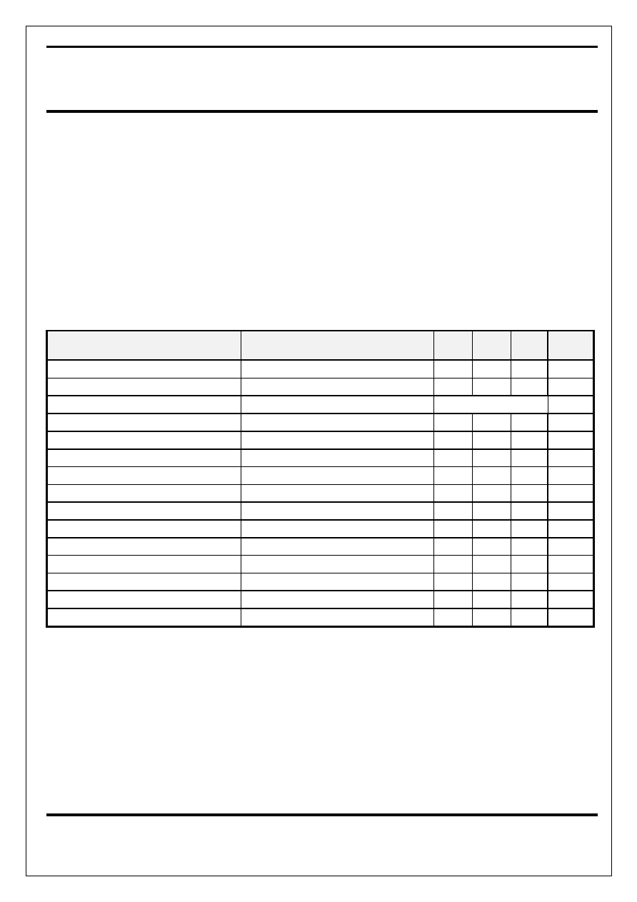
OUTPUT VOLTAGE
<Unless specified: V
CC
= 4.75V ~ 5.25V, GND = PGND = 0V, VOSENSE = V
O
, 0mV < (CS
+
- CS
-
) < 60mV, LDOV = 11.4V ~ 12.6V, T
A
= 25
∞
C>
-
Table 1
-
VID
4 3 2 1 0
Min.
(V)
Typ.
(V)
Max.
(V)
0 1 1 1 1
1.274
1.300
1.326
0 1 1 1 0
1.323
1.350
1.377
0 1 1 0 1
1.372
1.400
1.428
0 1 1 0 0
1.421
1.450
1.479
0 1 0 1 1
1.470
1.500
1.530
0 1 0 1 0
1.527
1.550
1.573
0 1 0 0 1
1.576
1.600
1.624
0 1 0 0 0
1.625
1.650
1.675
0 0 1 1 1
1.675
1.700
1.726
0 0 1 1 0
1.724
1.750
1.776
0 0 1 0 1
1.773
1.800
1.827
0 0 1 0 0
1.822
1.850
1.878
0 0 0 1 1
1.871
1.900
1.929
0 0 0 1 0
1.921
1.950
1.979
0 0 0 0 1
1.970
2.000
2.030
0 0 0 0 0
2.019
2.050
2.081
1 1 1 1 1
1.940
2.000
2.060
1 1 1 1 0
2.058
2.100
2.142
1 1 1 0 1
2.156
2.200
2.244
1 1 1 0 0
2.254
2.300
2.346
1 1 0 1 1
2.352
2.400
2.448
1 1 0 1 0
2.450
2.500
2.550
1 1 0 0 1
2.548
2.600
2.652
1 1 0 0 0
2.646
2.700
2.754
1 0 1 1 1
2.744
2.800
2.856
1 0 1 1 0
2.842
2.900
2.958
1 0 1 0 1
2.940
3.000
3.060
1 0 1 0 0
3.038
3.100
3.162
1 0 0 1 1
3.136
3.200
3.264
1 0 0 1 0
3.234
3.300
3.366
1 0 0 0 1
3.332
3.400
3.468
1 0 0 0 0
3.430
3.500
3.570
Note: I
O
= 2.0A in Application Circuit
5
5 Bit Programmable Synchronous
DC/DC Controller
NIKO-SEM
N1153
AUG-03-2001
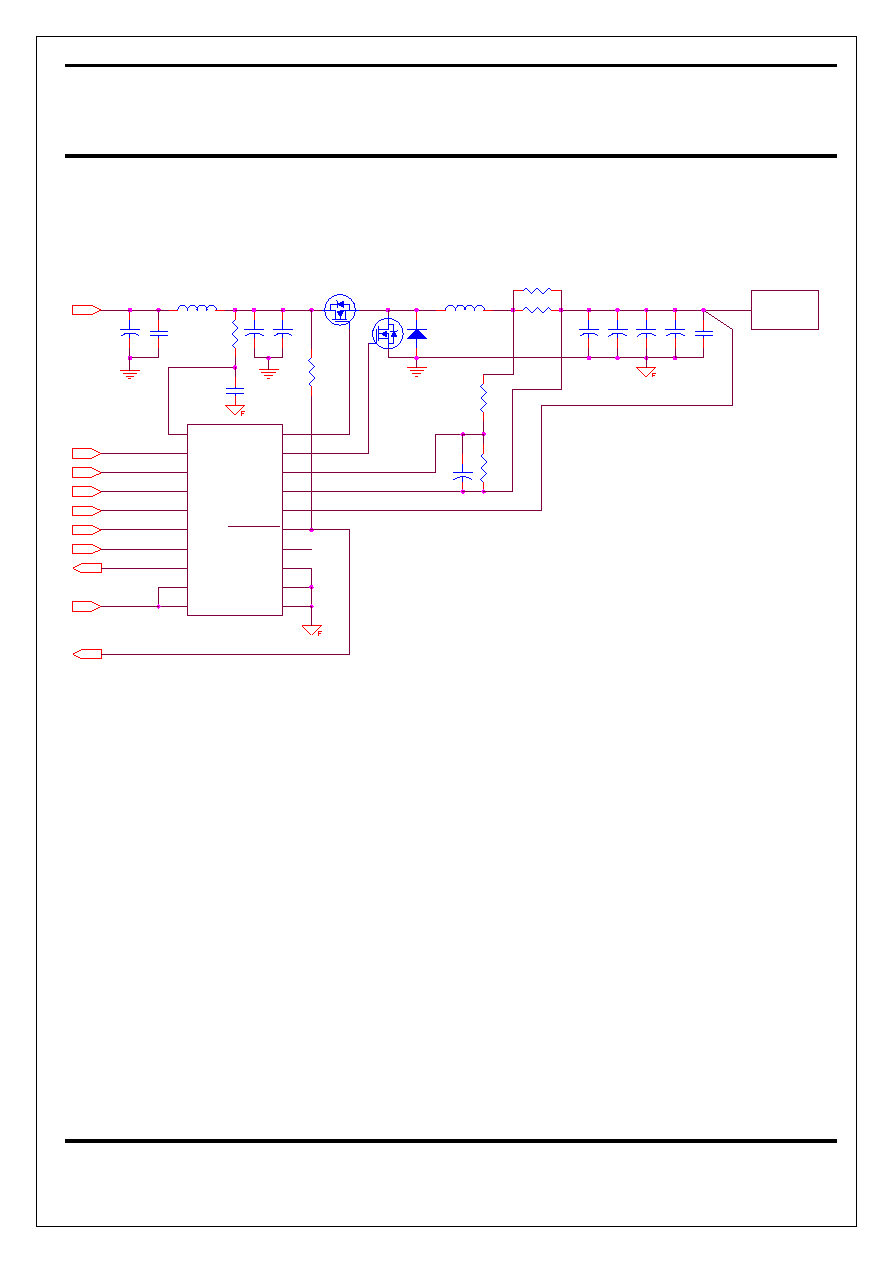
APPLICATION CIRCUIT
+
+
+
+
+
+
+
+
VID 0
VID 1
VID 2
VID 3
VID 4
P.G
12V
OVP
5V
S.D
VCORE
1000uF
4uH
SBD
P50N02L x 2
10K
0.1uF
10mOHM x 2
Mn-Cu Wire
1500uF x 4
MOSFET
1A/30V
0.1uF
1000uF x 2
2 uH
0.1uF
10
VID 0
VID 1
VID 2
VID 3
VID 4
POWERGOOD
OVP
GND
PGNDL
PGNDH
BSTH
BSTL
DH
DL
VCC
CS-
CS+
VO SENSE
SHUTDOWN
N1153
X
NC
1K
0.1uF
2.32K
6
5 Bit Programmable Synchronous
DC/DC Controller
NIKO-SEM
N1153
AUG-03-2001
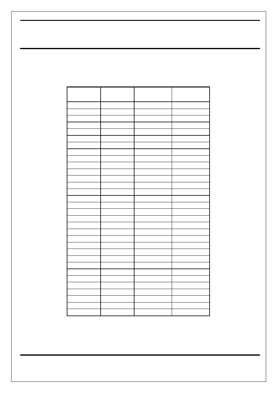
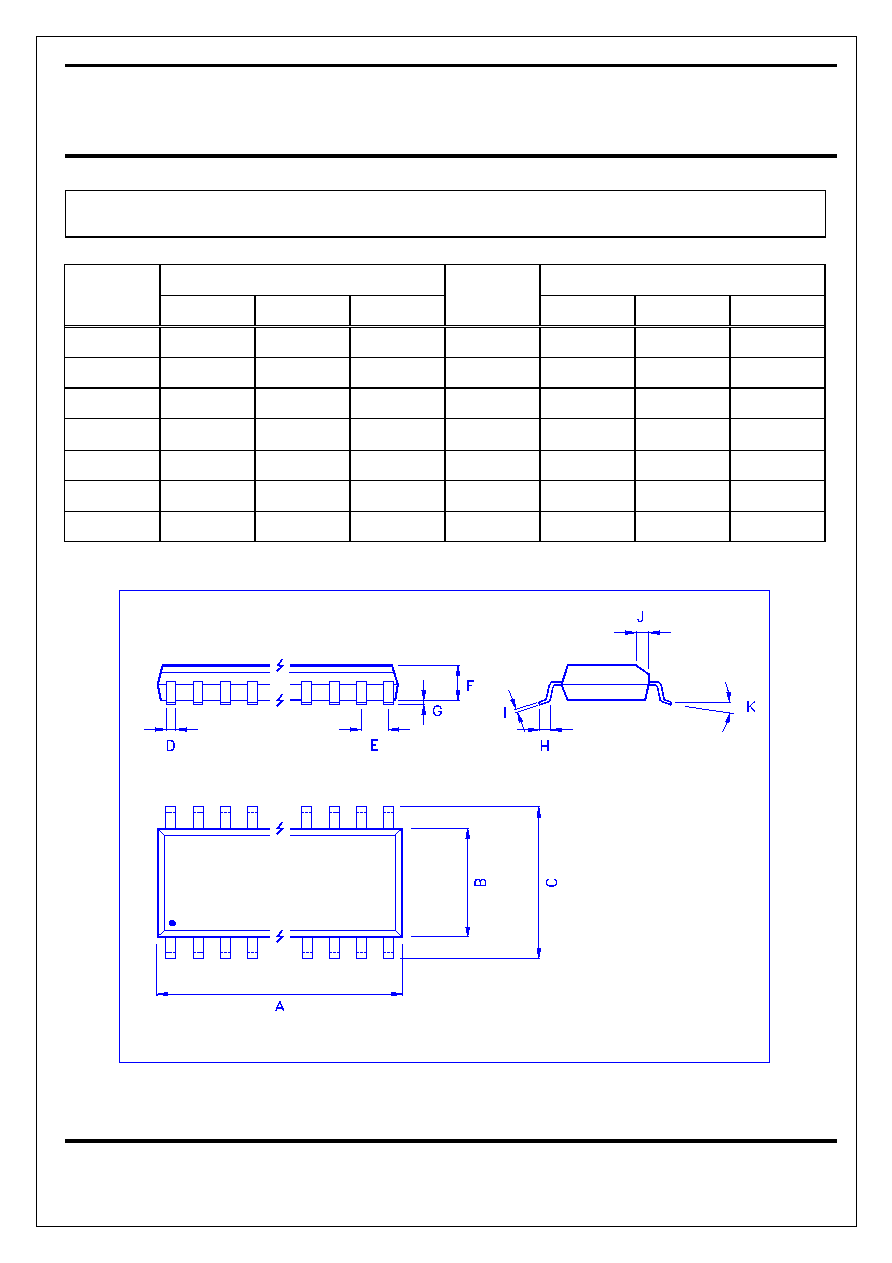
SOIC-20 (DW) MECHANICAL DATA
mm
mm
Dimension
Min. Typ. Max.
Dimension
Min. Typ. Max.
A 12.6 13.0 H 0.4 1.27
B 7.3 7.7 I 0.23 0.32
C 10 10.65 J 0.25 0.74
D 0.33 0.51 K 0
∞
8
∞
E
1.27
L
F
2.1
2.3
2.5
M
G
0.1
0.3
N