NanoAmp Solutions, Inc.
1982 Zanker Road, San Jose, CA 95112
ph: 408-573-8878, FAX: 408-573-8877
www.nanoamp.com
N32T1630C1E
(DOC # 14-02-006 Rev C ECN 01-1040
1
The specifications of this device are subject to change without notice. For latest documentation see http://www.nanoamp.com.
32Mb Ultra-Low Power Asynchronous CMOS PSRAM
2M x 16 bit
Overview
The N32T1630C1E is an integrated memory
device containing a 32 Mbit Pseudo Static Random
Access Memory using a self-refresh DRAM array
organized as 2,097,152 words by 16 bits. It is
designed to be identical in operation and interface
to standard 6T SRAMS. The device is designed for
low standby and operating current and includes a
power-down feature to automatically enter standby
mode. Also included are several other power
saving modes: a deep sleep mode where data is
not retained in the array and partial array refresh
mode where data is retained in a portion of the
array. Both these modes reduce standby current
drain. The device can operate over a very wide
temperature range of -25
o
C to +85
o
C.
Features
∑ Dual voltage for Optimum Performance:
Vccq - 2.7V to 3.3V
Vcc - 2.7V to 3.3V
∑ Fast Cycle Times
T
ACC
< 60 nS
T
ACC
< 70 nS
∑ Very low standby current
I
SB
< 120µA
∑ Very low operating current
Icc < 25mA
∑ Dual rail operation
V
CCQ
and V
SSQ
for separate I/O power rail
∑ Compact Space Saving BGA Package
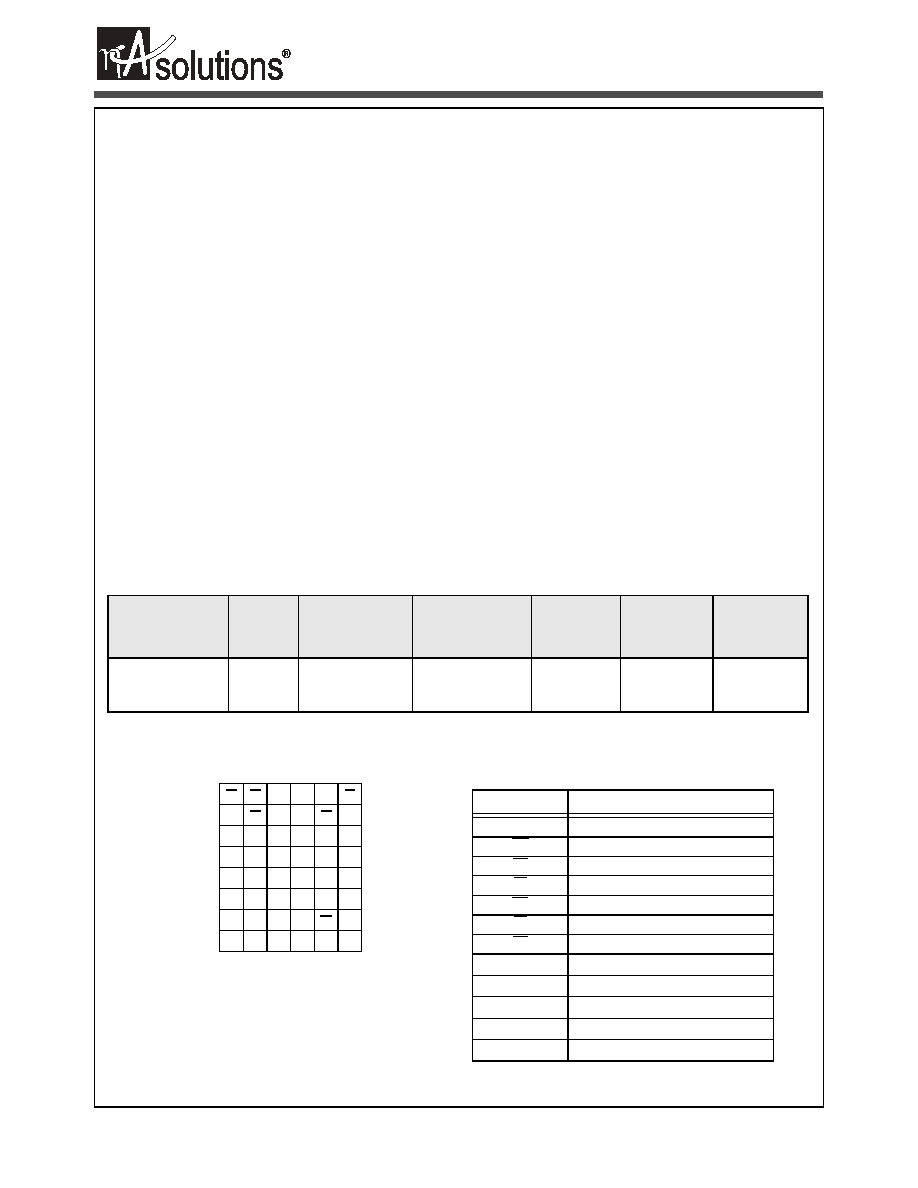
Figure 1: Pin Configuration
Product Family
Part Number
Package
Type
Operating
Temperature
Power
Supply
Speed
Standby
Current (I
SB
),
Max
Operating
Current (Icc),
Max
N32T1630C1EZ
48-BGA
-25
o
C to +85
o
C
2.7V - 3.3V(V
CC
)
60ns
70ns
120
µA
3 mA @ 1MHz
1
2
3
4
5
6
A
LB
OE
A
0
A
1
A
2
ZZ
B
I/O
8
UB
A
3
A
4
CE
I/O
0
C
I/O
9
I/O
10
A
5
A
6
I/O
1
I/O
2
D
V
SSQ
I/O
11
A
17
A
7
I/O
3
V
CC
E
V
CCQ
I/O
12
NC
A
16
I/O
4
V
SS
F
I/O
14
I/O
13
A
14
A
15
I/O
5
I/O
6
G
I/O
15
A
19
A
12
A
13
WE
I/O
7
H
A
18
A
8
A
9
A
10
A
11
A
20
48 Pin BGA (top)
6 x 8 mm
Table 1: Pin Descriptions
Pin Name
Pin Function
A
0
-A
20
Address Inputs
WE
Write Enable Input
CE
Chip Enable Input
ZZ
Deep Sleep Input
OE
Output Enable Input
LB
Lower Byte Enable Input
UB
Upper Byte Enable Input
I/O
0
-I/O
15
Data Inputs/Outputs
V
CC
Power
V
SS
Ground
V
CCQ
Power I/O only
V
SSQ
Ground I/O only

(DOC # 14-02-006 Rev C ECN 01-1040
2
The specifications of this device are subject to change without notice. For latest documentation see http://www.nanoamp.com.
NanoAmp Solutions, Inc.
N32T1630C1E
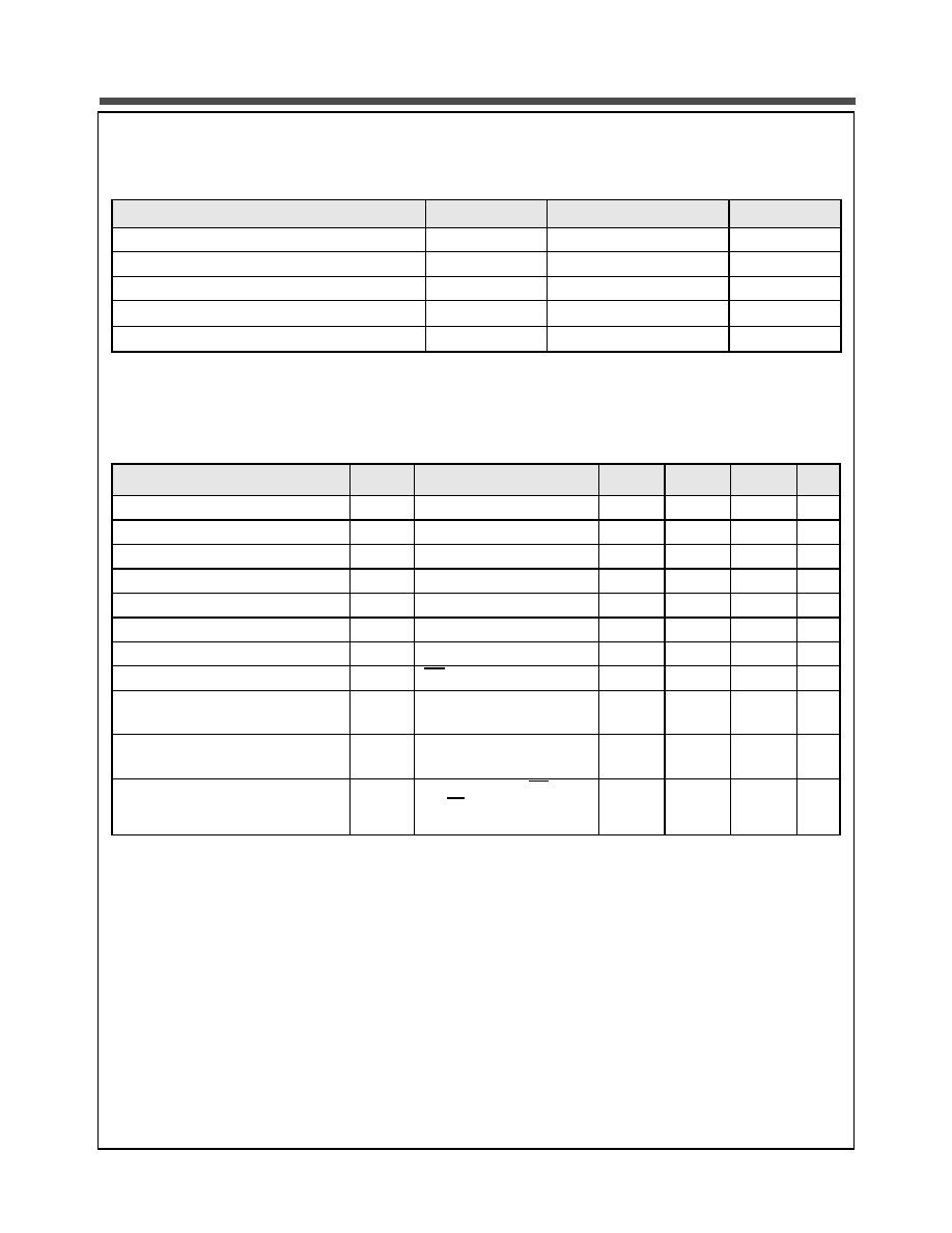
Functional Block Diagram
Functional Description
CE
WE
OE
UB/LB
ZZ
I/O
1
1. When UB and LB are in select mode (low), I/O
0
- I/O
15
are affected as shown. When LB only is in the select mode only
I/O
0
- IO
7
are affected as shown. When UB is in the select mode only I/O
8
- I/O
15
are affected as shown. If both UB and LB
are in the deselect mode (high), the chip is in a standby mode regardless of the state of CE.
MODE
POWER
H
X
X
X
H
High Z
Standby
2
2. When the device is in standby mode, control inputs (WE, OE, UB, and LB), address inputs and data input/outputs are
internally isolated from any external influence and disabled from exerting any influence externally.
Standby
X
X
X
H
H
High Z
Standby
2
Standby
L
L
X
3
L
1
H
Data In
Write
3
3. When WE is invoked, the OE input is internally disabled and has no effect on the circuit.
Active
L
H
L
L
1
H
Data Out
Read
Active
L
H
H
L
1
H
High Z
Output Disabled
Active
H
X
X
X
L
High Z
Low Power Modes
Low Power
Capacitance
1
1. These parameters are verified in device characterization and are not 100% tested
Item
Symbol
Test Condition
Min
Max
Unit
Input Capacitance
C
IN
V
IN
= 0V, f = 1 MHz, T
A
= 25
o
C
8
pF
I/O Capacitance
C
I/O
V
IN
= 0V, f = 1 MHz, T
A
= 25
o
C
8
pF
Control
Logic
Decode
Logic
Address
Inputs
A
0
- A
20
CE
WE
OE
Input/
Output
Mux
and
Buffers
I/O
0
- I/O
7
UB
LB
I/O
8
- I/O
15
Address
2048K x 16
Memory
Array
ZZ
(DOC # 14-02-006 Rev C ECN 01-1040
3
The specifications of this device are subject to change without notice. For latest documentation see http://www.nanoamp.com.
NanoAmp Solutions, Inc.
N32T1630C1E
Absolute Maximum Ratings
1
1. Stresses greater than those listed above may cause permanent damage to the device. This is a stress rating only and functional
operation of the device at these or any other conditions above those indicated in the operating section of this specification is not
implied. Exposure to absolute maximum rating conditions for extended periods may affect reliability.
Item
Symbol
Rating
Unit
Voltage on any pin relative to V
SS
V
IN,OUT
≠0.2 to V
CC
+0.3
V
Voltage on V
CC
Supply Relative to V
SS
V
CC
≠0.2 to 3.6
V
Power Dissipation
P
D
1
W
Storage Temperature
T
STG
≠65 to 125
o
C
Operating Temperature
T
A
-25 to +85
o
C
Operating Characteristics (Over Specified Temperature Range)
Item
Symbol
Comments
Min.
Typ
1
1. Typical values are measured at Vcc=Vcc Typ., T
A
=25∞C and not 100% tested.
Max.
Unit
Supply Voltage
V
CC
2.7
3.0
3.3
V
Supply Voltage for I/O
V
CCQ
2.7
3.0
3.3
V
Input High Voltage
V
IH
0.8V
CCQ
V
CC
+0.2
V
Input Low Voltage
V
IL
≠0.2
0.2V
CCQ
V
Output High Voltage
V
OH
I
OH
= -0.5mA
0.8V
CCQ
V
Output Low Voltage
V
OL
I
OL
= 0.5mA
0.2V
CCQ
V
Input Leakage Current
I
LI
V
IN
= 0 to V
CC
-1
1
µA
Output Leakage Current
I
LO
OE = V
IH
or Chip Disabled
-1
1
µA
Read/Write Operating Supply Current
@ 1
µs Cycle Time
2
2. This parameter is specified with the outputs disabled to avoid external loading effects. The user must add current required to drive
output capacitance expected in the actual system.
I
CC1
V
CC
=V
CC
MAX, V
IN
=V
IH
/ V
IL
Chip Enabled, I
OUT
= 0
3
mA
Read/Write Operating Supply Current
@ Min Cycle Time
2
I
CC2
V
CC
=V
CC
MAX, V
IN
=V
IH
/ V
IL
Chip Enabled, I
OUT
= 0
25
mA
Standby Current
I
SB
Chip deselected, CE>VCC-
0.2, ZZ>VCC-0.2 and VIN =
0 or VCC
120
µA
(DOC # 14-02-006 Rev C ECN 01-1040
4
The specifications of this device are subject to change without notice. For latest documentation see http://www.nanoamp.com.
NanoAmp Solutions, Inc.
N32T1630C1E
Output Load Circuit
Power Up Sequence
After applying power, maintain a stable power supply for a minimum of 200us after CE > VIH.
Timing Test Conditions
Item
Input Pulse Level
0.1V
CC
to 0.9 V
CC
Input Rise and Fall Time
5ns
Input and Output Timing Reference Levels
0.5 V
CC
Operating Temperature
-25
o
C to +85
o
C
50 pF
I/O
Output Load
(DOC # 14-02-006 Rev C ECN 01-1040
5
The specifications of this device are subject to change without notice. For latest documentation see http://www.nanoamp.com.
NanoAmp Solutions, Inc.
N32T1630C1E
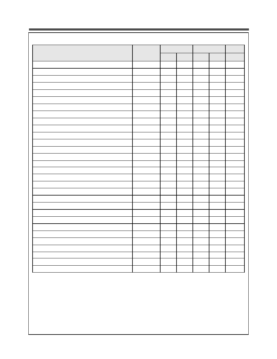
Do not access device with invalid cycle time (shorter than tRC, tWC) for a continous period > 20us.
Timings
Item
Symbol
-60
-70
Units
Min.
Max.
Min.
Max.
Read Cycle Time
t
RC
60
20000
70
20000
ns
Address Access Time
t
AA
60
70
ns
Page Mode Read Cycle Time
t
PC
25
20000
25
20000
ns
Page Mode Access Time
t
PA
25
25
ns
Chip Enable to Valid Output
t
CO
60
70
ns
Output Enable to Valid Output
t
OE
25
25
ns
Byte Select to Valid Output
t
LB
, t
UB
60
70
ns
Chip Enable to Low-Z output
t
LZ
10
10
ns
Output Enable to Low-Z Output
t
OLZ
5
5
ns
Byte Select to Low-Z Output
t
BZ
10
10
ns
Chip Disable to High-Z Output
t
HZ
0
5
0
5
ns
Output Disable to High-Z Output
t
OHZ
0
5
0
5
ns
Byte Select Disable to High-Z Output
t
BHZ
0
5
0
5
ns
Output Hold from Address Change
t
OH
5
5
ns
Write Cycle Time
t
WC
60
20000
70
20000
ns
Page Mode Write Cycle Time
t
PWC
25
20000
25
20000
ns
Chip Enable to End of Write
t
CW
50
60
ns
Address Valid to End of Write
t
AW
50
60
ns
Byte Select to End of Write
t
BW
50
60
ns
Write Pulse Width
t
WP
50
50
ns
Write Recovery Time
t
WR
0
0
ns
Write to High-Z Output
t
WHZ
5
5
ns
Address Setup Time
t
AS
0
0
ns
Data to Write Time Overlap
t
DW
20
20
ns
Data Hold from Write Time
t
DH
0
0
ns
End Write to Low-Z Output
t
OW
5
5
ns
Maximum Page Mode Cycle
t
PGMAX
20000
20000
ns
Chip Enable High Pulse Width
t
CP
10
10
ns