 | –≠–ª–µ–∫—Ç—Ä–æ–Ω–Ω—ã–π –∫–æ–º–ø–æ–Ω–µ–Ω—Ç: NT3883F | –°–∫–∞—á–∞—Ç—å:  PDF PDF  ZIP ZIP |
NT3883
Dot Matrix LCD 80-Channel Driver
1
V2.1 November, 1999
Features
T
Provides 80-channel LCD driver
T
Internal serial to parallel conversion circuits:
40-bit bi-direction shift register
2
80-bit latch
1
80-bit 4-level driver
1
T
Logic circuit supply voltage range: 4.5V - 5.5V
T
LCD driving voltage range (V
DD
- V
EE
): 3.5V to 11V
T
Applicable LCD duty cycle: 1/2 to 1/16
T
Interfaces with a NT3881B/C/D LCD controller
T
LCD bias voltage can be supplied externally
T
Available in 100-pin QFP and in CHIP FORM
General Description
The NT3883 is a dot matrix LCD 80-channel driver
fabricated by low power CMOS technology. This IC
consists of two 40-bit bi-directional shift registers, 80-bit
latch and 80-bit 4-level LCD driver. The NT3883 converts
serial data that are received from the LCD controller, such
as NT3881B/C/D, to parallel data and outputs LCD driving
waveforms to drive LCD. Expansion of character-type
liquid crystal display can be easily obtained according to
the number and structure of characters.
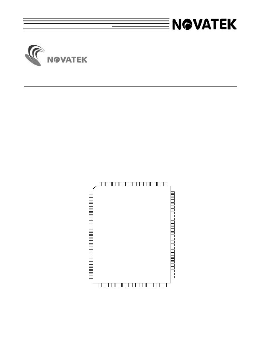
Pin Configuration
100
S
3
1
93
99
92
86
83
81
87
84
98
82
94
96
85
90 89 88
97
91
95
S
7
1
S
7
2
S
7
3
S
7
4
S
7
5
S
7
6
S
7
7
S
7
8
S
7
9
S
8
0
S
4
0
S
3
9
S
3
8
S
3
7
S
3
6
S
3
5
S
3
4
S
3
3
S
3
2
N T 3 8 8 3 F
S18
S19
S20
S21
S22
S23
S24
S25
S26
S27
S28
S29
S30
S3
S4
S5
S6
S7
S8
S9
S10
S11
S12
S13
S14
S15
S16
S17
S1
S2
1
2
18
8
7
11
9
5
6
3
4
10
17
15
16
14
13
12
20
19
27
28
29
30
25
24
23
22
21
26
S58
S59
S60
S61
S62
S63
S64
S65
S66
S67
S68
S69
S70
S43
S44
S45
S46
S47
S48
S49
S50
S51
S52
S53
S54
S55
S56
S57
S41
S42
80
79
63
73
74
70
72
76
75
78
77
71
64
66
65
67
68
69
61
62
54
53
52
51
56
57
58
59
60
55
31
38
32
39
45
48
50
44
47
33
49
37
35
46
41 42 43
34
40
36
V
E
E
N
C
N
C
M
D
R
2
D
L
2
D
R
1
D
L
1
C
L
2
N
C
N
C
N
C
S
L
2
S
L
1
C
L
1
G
N
D
V
2
V
3
V
D
D
N
C
NT3883
2
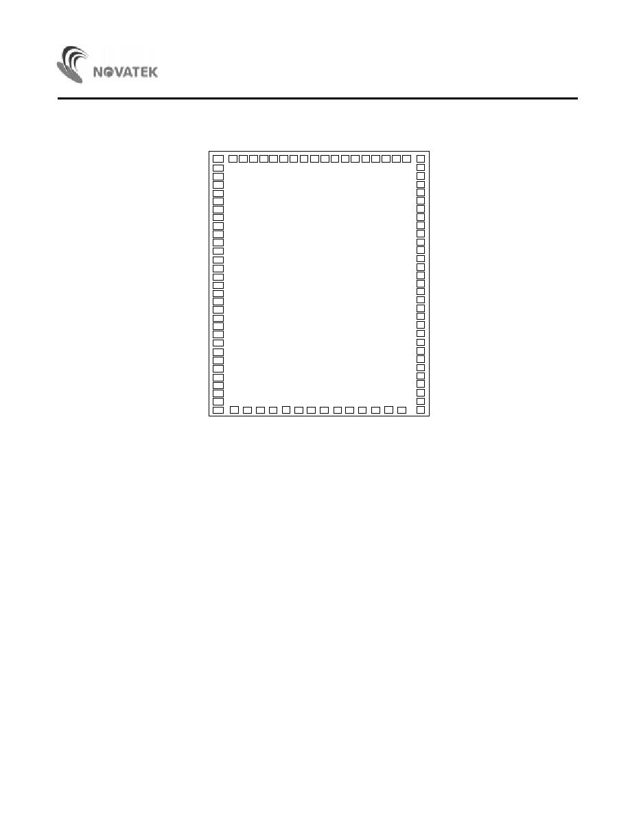
Pad Configuration
81
80
79
78
77
76
75
74
73
72
71
70
69
68
67
66
65
64
63
62
61
60
59
58
57
56
55
54
53
95
31
33
34
35
36
37
38
39
43
44
45
46
47
48
51
52
94 93
92 91
90 89
88
99
98 97
96
87
86 85
84 83
82
NT3883H
S31
S18
S19
S20
S21
S22
S23
S24
S25
S26
S27
S28
S29
S30
S 2
S 3
S 4
S 5
S 6
S 7
S12
S13
S14
S15
S16
S17
S 8
S 9
S10
S11
S 1
100
1
2
3
4
5
6
7
8
9
10
11
12
13
14
15
16
17
18
19
20
21
22
23
24
25
26
27
28
29
30
S
3
2
S
3
9
S
3
8
S
3
7
S
3
6
S
3
5
S
3
4
S
3
3
S
4
0
S
7
4
S
7
5
S
7
6
S
7
7
S
7
8
S
7
9
S
8
0
S
7
2
S
7
3
M
D
R
2
D
L
2
D
R
1
D
L
1
C
L
2
S
L
2
S
L
1
G
L
1
G
N
D
V
2
V
3
V
D
D
V
E
E
S71
S58
S59
S60
S61
S62
S63
S64
S65
S66
S67
S68
S69
S70
S52
S53
S54
S55
S56
S57
S51
S47
S48
S49
S50
S46
S42
S43
S44
S45
S41
NT3883
3
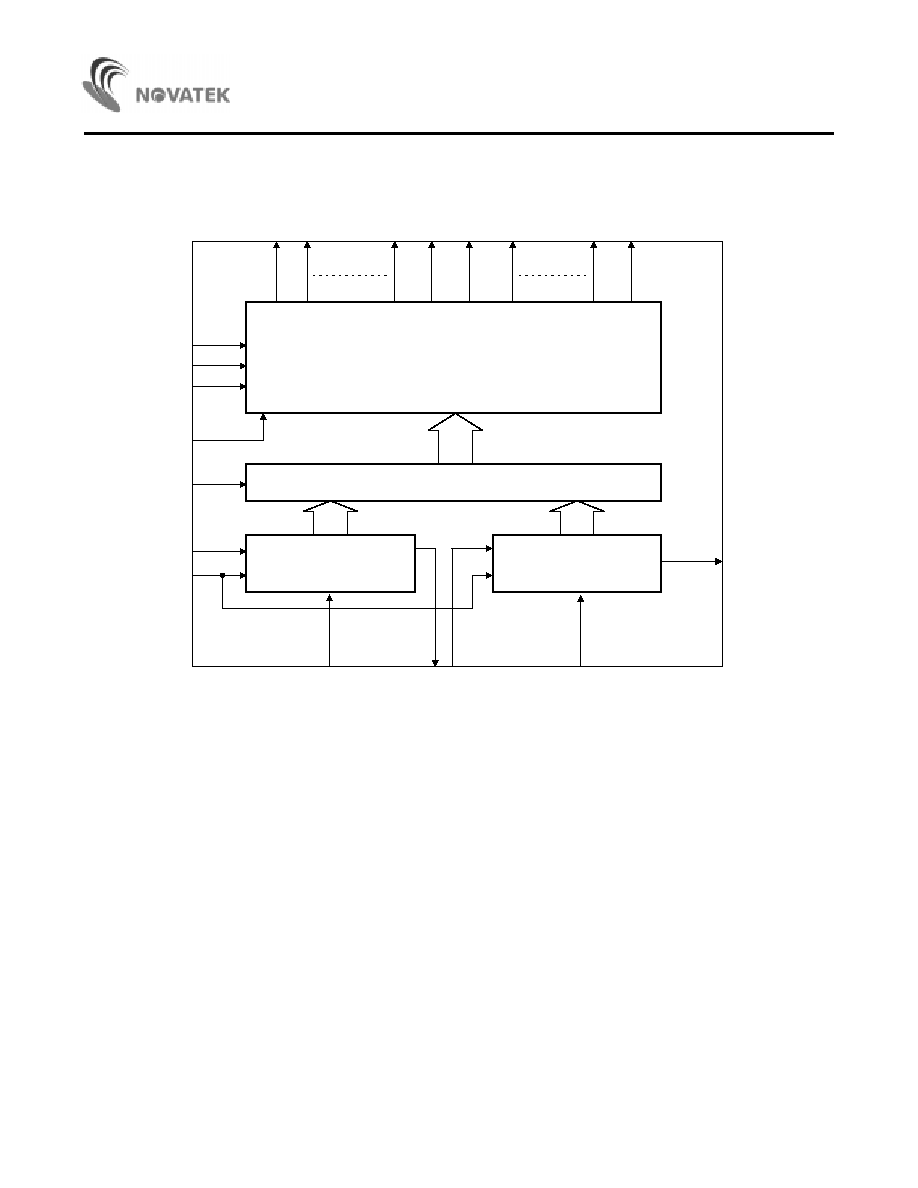
Block Diagram
80-Bit 4-Level LCD Drivers
80-Bit Latch
First
40-Bit Shift Register
Second
40-Bit Shift Register
S1
S2
S39
S40
S41
S42
S79
S80
DR2
G N D
DL2
DR1
CL2
DL2
CL1
M
V
E E
V
3
V
2
V
DD
SL1
SL2
NT3883
4
Absolute Maximum Ratings*
Power Supply Voltage (V
DD
-GND) . . . . . . -0.3V to 7.0V
Power Supply Voltage (V
DD
-V
EE
) . . . . . . . . . . . . . . . . . .
. . . . . . . . . . . . . . . . . . . . . .V
DD
- 13.5V to V
DD
+ 0.3V
Input Voltage . . . . . . . . . . . . . . -0.3V to V
DD
+ 0.3V
Operating Temperature . . . . . . . . . . -20
G
C to + 75
G
C
Storage Temperature . . . . . . . . . . . . . -55
G
C to + 125
G
C
*Comments
Stresses above those listed under "Absolute Maximum
Ratings" may cause permanent damage to this device.
These are stress ratings only. Functional operation of
this device at these or any other conditions above those
indicated in the operational sections of this specification
is not implied and exposure to the absolute maximum
rating conditions for extended periods may affect device
reliability.
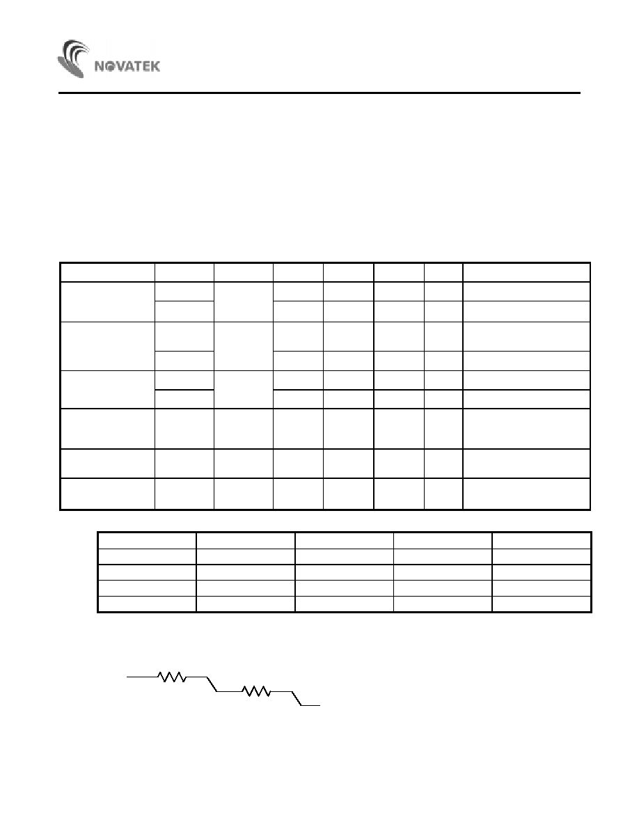
DC Electrical Characteristics (V
DD
= 5.0V, GND = 0V, V
EE
= 0V, T
A
= 25
G
C)
Parameter
Symbol
Terminal
Min.
Typ.
Max.
Unit
Conditions
Input Voltage
V
IH
0.7 V
DD
-
V
DD
V
V
IL
CL1, CL2,
DL1, DL2
*1
0
-
0.3 V
DD
V
Output Voltage
V
OH
DR1, DR2
*1
V
DD
- 0.4
-
-
V
I
OH
= -0.4mA
V
OL
-
-
0.4
V
I
OL
= +0.4mA
Vi - Sj Voltage
V
D1
-
-
1.1
V
I
ON
= 0.1mA for one of Sj
Descending
V
D2
*2
-
-
1.5
V
I
ON
= 0.05mA for each of Sj
Input Leakage
Current
I
IL
CL1, CL2
DL1,
DL2*1
-5
-
5
2
A
V
IN
= 0 or V
DD
Vi Leakage
Current
I
VL
V
2
, V
3
, V
EE
-10
-
10
2
A
S1 to S80 open
Power Supply
Current
I
DD
*3
-
-
500
2
A
f
CL1
= 1KHz
f
CL2
= 1MHz
Note *1: SL1 and SL2 determine The Input or Output of DL1, DL2, DR1 and DR2 and the configuration is as follows.
Terminal
SL1 = High
SL1 = Low
SL2 = High
SL2 = Low
DL1
Output
Input
-
-
DR1
Input
Output
-
-
DL2
-
-
Output
Input
DR2
-
-
Input
Output
*2: V
i
≠ S
j
(V
i
= V
DD
, V
2
, V
3
, V
EE
; j = 1 to 80) equivalent circuit (for reference)
*3: Input/output current is excluded. When the input is at the intermediate level with CMOS, some excessive
V
i
1Kmax.
10Kmax.
Power
Switch
Data
Swtich
S
j
Current will flow through the input circuit to power supply. To avoid this, the input level must be fixed at high or
low state.
NT3883
5
AC Characteristics (V
DD
= 5.0V, GND = 0V, V
EE
= 0V, T
A
= 25
G
C)
Parameter
Symbol
Terminal
Min.
Typ.
Max.
Unit
Data Shift Frequency
f
CL2
CL2
-
-
400
KHz
High
t
CW H
CL1, CL2
800
-
-
ns
Clock Width
Low
t
CW L
CL2
800
-
-
ns
Data Hold Time
t
DH
DL1~2, DR1~2
300
-
-
ns
Data Set-up Time
t
SUD
DL1~2, DR1~2
300
-
-
ns
Clock Set-up Time(CL2
CL1)
t
SUC1
CL1, CL2
500
-
-
ns
Clock Set-up Time(CL1
CL2)
t
SUC2
CL1, CL2
500
-
-
ns
Clock Rise/Fall Time
t
CL
CL1, CL2
-
-
200
ns
Data Delay Time
t
PD
-
-
-
500
ns
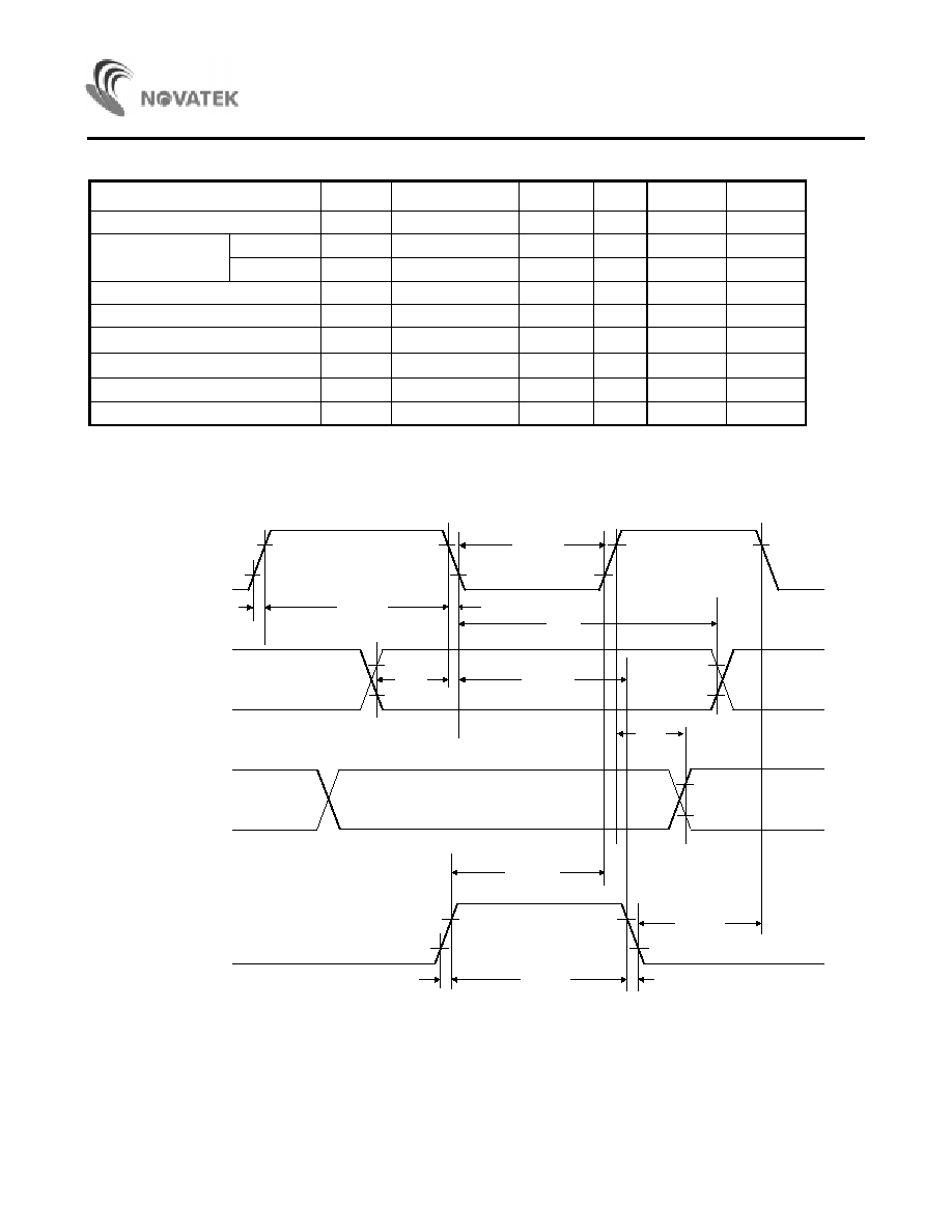
Timing Waveforms
t
CL
V
IH
V
IL
t
CL
t
CWH
t
CWL
t
CL
t
DH
t
SUD
t
SUC1
t
PD
t
SUC2
t
SUC2
t
CWH
t
CL
V
OH
V
OL
CL2
DL1, DL2
DR1, DR2
CL1
NT3883
6
Pin and Pad Descriptions
Pin No.
Pad No.
Designation
I/O
External
Connection
Description
1~30,
51~100
1~30,
51~100
S1~S30,
S80~S31
O
LCD panel
Segment signal output pins
33
33
V
DD
P
Power supply
Power for logic circuits
36
36
GND
P
Power supply
0V
37
37
CL1
I
Controller
Clock to latch serial data
38
38
SL1
I
MPU
Shift left control for 1st 40-bit shift register
(see NOTE*4)
39
39
SL2
I
MPU
Shift left control for 1st 40-bit shift register
(see NOTE*4)
43
43
CL2
I
Controller
Clock to shift serial data
44
44
DL1
I/O
Controller or
NT3882A/NT3
883
Data input/output of 1st 40-bit shift register
(see NOTE*4)
45
45
DR1
I/O
Controller or
NT3882A/NT3
883
Data input/output of 1st 40-bit shift register
(see NOTE*4)
46
46
DL2
I/O
Controller or
NT3882A/NT3
883
Data input/output of 2nd 40-bit shift register
(see NOTE*4)
47
47
DR2
I/O
Controller or
NT3882A/NT3
883
Data input/output of 2nd 40-bit shift register
(see NOTE*4)
48
48
M
I
Controller
Alternate signal for LCD drivers
31, 34, 35
31, 34, 35
V
EE
, V
3
, V
2
P
Power supply
Power for LCD drivers
32, 40,
41, 42,
49,50
-
NC
-
-
No connection
NOTE *4: Relation of SL1, SL2, DL1, DR1, DL2 and DR2
SL1
SL2
Shift Direction
DL1
DR1
DL2
DR2
1(High)
-
Left(S40 to S1)
Output
Input
-
-
0(Low)
-
Right(S1 to S40)
Input
Output
-
-
-
1(High)
Left(S80 to S41)
-
-
Output
Input
-
0(Low)
Right(S41 to S80)
-
-
Input
Output
NT3883
7
Functional Description
NT3883 is a dot matrix LCD segment driver LSI. It
operates with the controller, such as NT3881B/C/D,
and/or another segment driver LSI NT3882A/3883.
NT3883 receives serial data from the controller or
another NT3883, converts it to parallel data and then
supplies the LCD driving waveforms to the LCD panel.
1. CL1
This signal is used for latching the shift register contents.
When CL1 is set at high, the shift register contents are
transferred to the 80-bit 4level LCD driver. When CL1 is
set at low, the last display output data (S1 to S80) is
held.
2. CL2
Clock pulse inputs for the two 40-bit shift registers. The
data is shifted to an 80-bit latch at the falling edge of
CL2. The clock signal CL2 must be active when
operating to refresh shift registers' contents.
3. DL1
Data input/output of the 1
st
- 40
th
register. When SL1 is
connected to GND or open, the data from LCD controller
is fed into the 1
st
- 40
th
register through DL1 serially. If
SL1 is connected to V
DD
, the DL1 becomes the output of
the 1
st
- 40
th
register.
4. DR1
Data input/output of the 1
st
- 40
th
register. When SL1 is
connected to GND, the 20
th
bit of the 1
st
- 40
th
register
output from DR1. By connecting DR1 to DL2, two 40-bit
shift registers cascaded to one 80-bit shift register. If
SL1 is connected to V
DD
, the DR1 becomes the input of
the 1
st
- 40
th
register, in this case, the data may come
from DL2.
5. DL2
Data input/output of the 41
st
- 80
th
register. When SL2 is
connected to GND, the data from LCD controller is fed
into the 41
st
- 80
th
register through DL2 serially. If SL2 is
connected to V
DD
, the DL2 becomes the output of the
41
st
- 80
th
register.
6. DR2
Data input/output of the 41
st
- 80
th
register. When SL2 is
connected to GND, the 80
th
bit of the 41
st
- 80
th
register
output from DR2. By connecting DR2 to DL1 of next
NT3882A/3883, the cascade structure is obtained to
drive a wider LCD panel. If SL2 is connected to V
DD
, the
DR2 becomes the input of the 41
st
- 80
th
register, in this
case, the data may come from the next NT3882A/3883.
7. SL1
The shift direction of S1 to S40, i.e. 1
st
to 40
th
shift
register, is selected by SL1. The detail function
description is listed in Note*4 of Page5.
8. SL2
The shift direction of S41 to S80, i.e. 41
st
to 80
th
shift
register, is selected by SL2. The detail function
description is listed in Note*4 of Page5.
9. S1 to S80
LCD driver output pins. These 80 bits represent the 80
data bits in the 80-bit latch and one of V
DD
, V
2
, V
3
and
V
EE
is selected as a LCD driving voltage source
according to the combination of latched data level and
the alternate signal (M). The truth table is listed as
follows:
Latched Data
M
Output Level of S1 to S80
1(High)
V
EE
1(High)
(Selected)
0(Low)
V
DD
1(High)
V
3
0(Low)
(Non-selected)
0(Low)
V
2
NT3883
8
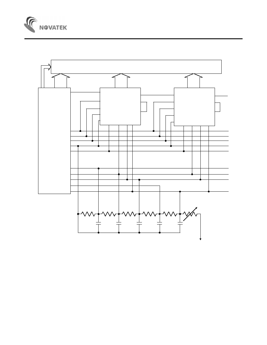
Application Circuit
(for reference only)
20 Chars x 4 Lines LCD PANEL
NT3881D
NT3883
NT3883
C 1 - C 1 6
S1 - S40
D
C L 2
C L 1
M
V
DD
G N D
V
1
V
2
V
3
V
4
V
5
D L 1
C L 2
C L 1
M
V
DD
G N D
V
2
V
3
V
EE
D R 1
D L 2
D R 2
S1 - S80
S1 - S80
D R 2
D L 2
D R 1
V
EE
V
3
V
2
G N D
V
DD
M
C L 1
C L 2
D L 1
R
R
R
R
R
V R
C
C
C
C
C
G N D o r o t h e r
negative voltage
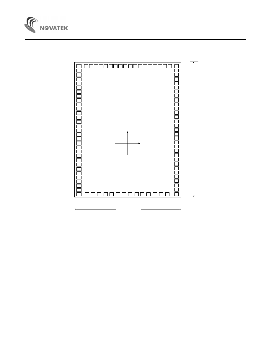
NT3883
9
Bonding Diagram
95
31
33
34
35
36
37
38
39
43
44
45
46
47
48
S71
S58
S59
S60
S61
S62
S63
S64
S65
S66
S67
S68
S69
S70
S52
S53
S54
S55
S56
S57
S51
S47
S48
S49
S50
S46
S42
S43
S44
S45
94
93
92
91
90
89
88
99
98
97
96
87
86
85
84
83
82
S41
N T 3 8 8 3 H
Y
X
(0,0)
S
3
2
S
3
9
S
3
8
S
3
7
S
3
6
S
3
5
S
3
4
S
3
3
S
4
0
S
7
4
S
7
5
S
7
6
S
7
7
S
7
8
S
7
9
S
8
0
S
7
2
S
7
3
81
80
79
78
77
76
75
74
73
72
71
70
69
68
67
66
65
64
63
62
61
60
59
58
57
56
55
54
53
51
52
100
1
2
3
4
5
6
7
8
9
10
11
12
13
14
15
16
17
18
19
20
21
22
23
24
25
26
27
28
29
30
3 9 4 0
2
m
2 5 9 0
2
m
M
D
R
2
D
L
2
D
R
1
D
L
1
C
L
2
S
L
2
S
L
1
G
L
1
G
N
D
V
2
V
3
V
D
D
V
E
E
S31
S18
S19
S20
S21
S22
S23
S24
S25
S26
S27
S28
S29
S30
S2
S3
S4
S5
S6
S7
S12
S13
S14
S15
S16
S17
S8
S9
S10
S11
S1
* Connecting IC substrate to V
DD
or keeping floating is recommended.
* Pad window area 100
2
m
100
2
m.
NT3883
10
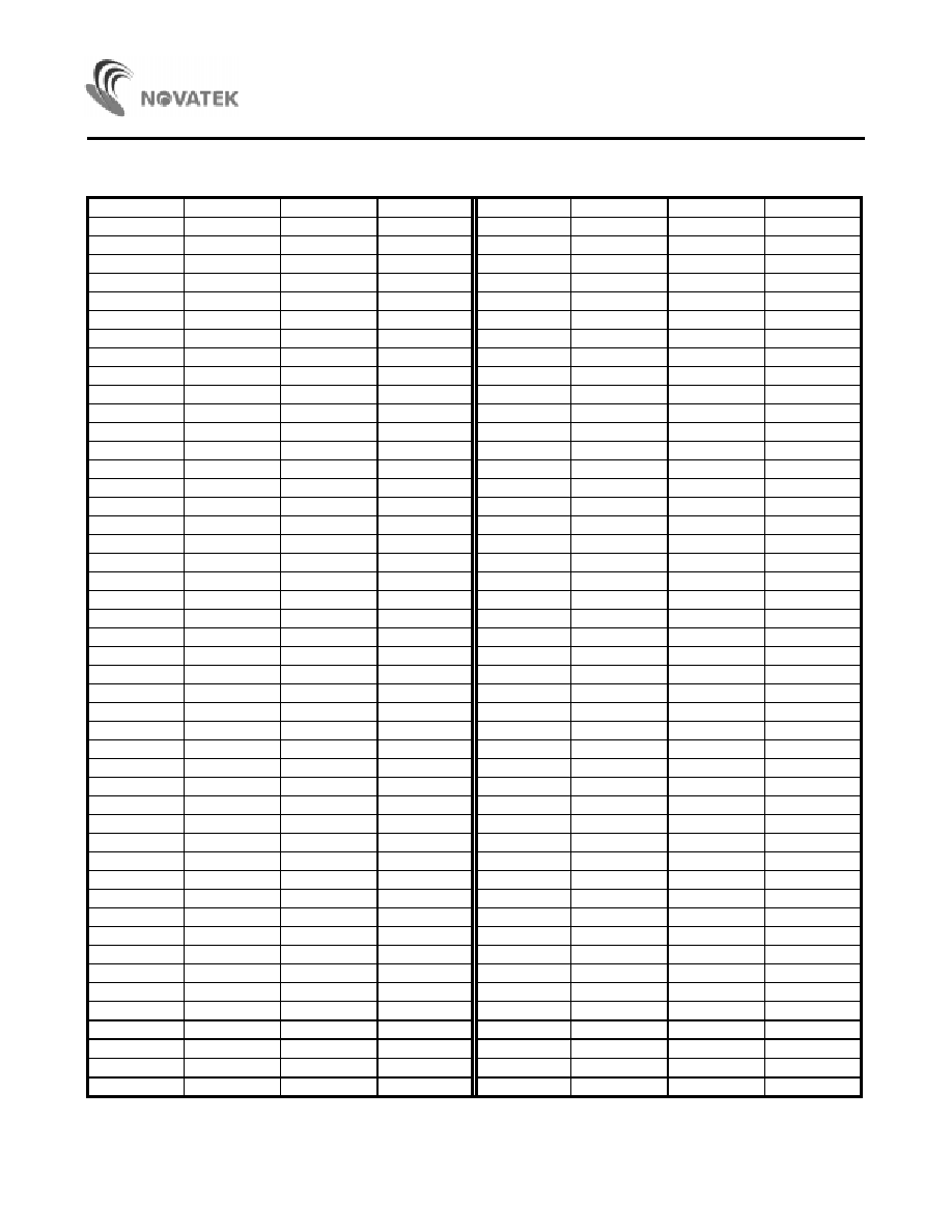
Bonding Dimensions
unit:
2
m
Pad No.
Designation
X
Y
Pad No.
Designation
X
Y
1
S30
-1194
1677
54
S44
1195
-1442
2
S29
-1194
1557
55
S45
1195
-1311
3
S28
-1194
1437
56
S46
1195
-1202
4
S27
-1194
1317
57
S47
1195
-1082
5
S26
-1194
1197
58
S48
1195
-962
6
S25
-1194
1077
59
S49
1195
-842
7
S24
-1194
957
60
S50
1195
-722
8
S23
-1194
837
61
S51
1195
-602
9
S22
-1194
717
62
S52
1195
-482
10
S21
-1194
597
63
S53
1195
-362
11
S20
-1194
477
64
S54
1195
-242
12
S19
-1194
357
65
S55
1195
-122
13
S18
-1194
237
66
S56
1195
-2
14
S17
-1194
117
67
S57
1195
117
15
S16
-1194
-2
68
S58
1195
237
16
S15
-1194
-122
69
S59
1195
357
17
S14
-1194
-242
70
S60
1195
477
18
S13
-1194
-362
71
S61
1195
597
19
S12
-1194
-482
72
S62
1195
717
20
S11
-1194
-602
73
S63
1195
837
21
S10
-1194
-722
74
S64
1195
957
22
S9
-1194
-842
75
S65
1195
1077
23
S8
-1194
-962
76
S66
1195
1197
24
S7
-1194
-1082
77
S67
1195
1317
25
S6
-1194
-1202
78
S68
1195
1437
26
S5
-1194
-1322
79
S69
1195
1557
27
S4
-1194
-1442
80
S70
1195
1677
28
S3
-1194
-1562
81
S71
1185
1811
29
S2
-1194
-1682
82
S72
995
1821
30
S1
-1184
-1812
83
S73
875
1821
31
VEE
-945
-1822
84
S74
755
1821
33
VDD
-807
-1822
85
S75
635
1821
34
V3
-670
-1822
86
S76
515
1821
35
V2
-520
-1822
87
S77
395
1821
36
GND
-353
-1822
88
S78
275
1821
37
CL1
-204
-1822
89
S79
155
1821
38
SL1
-54
-1822
90
S80
35
1821
39
SL2
95
-1822
91
S40
-84
1821
43
CL2
245
-1822
92
S39
-204
1821
44
DL1
395
-1822
93
S38
-324
1821
45
DR1
545
-1822
94
S37
-444
1821
46
DL2
695
-1822
95
S36
-564
1821
47
DR2
845
-1822
96
S35
-684
1821
48
M
995
-1822
97
S34
-805
1821
51
S41
1185
-1812
98
S33
-925
1821
52
S42
1195
-1682
99
S32
-1045
1821
53
S43
1195
-1562
100
S31
-1184
1811

NT3883
11
Ordering Information
Part No.
Package
NT3883H
CHIP FORM
NT3883F
100L QFP
NT3883
12
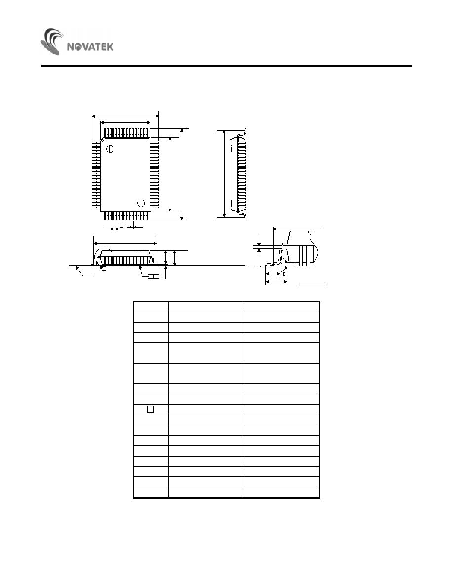
Package Information
QFP 100L Outline Dimensions
unit: inches/mm
A
1
A
2
A
Seating Plane
1
2 4
b
2 5
4 0
4 1
6 4
6 5
8 0
E
e
G
E
G
D
See Detail F
Detail F
D
H
D
H
E
D
y
L
G
D
~ ~~
L
1
c
Symbol
Dimensions in inches
Dimensions in mm
A
0.130 Max.
3.30 Max.
A
1
0.004 Min.
0.10 Min.
A
2
0.112±0.005
2.85±0.13
b
0.014 +0.004
0.35 +0.10
-0.002
-0.05
c
0.006 +0.004
0.15 +0.10
-0.002
-0.05
D
0.551±0.005
14.00±0.13
E
0.787±0.005
20.00±0.13
e
0.031±0.006
0.80±0.15
G
D
0.693 NOM.
17.60 NOM.
G
E
0.929 NOM.
23.60 NOM.
H
D
0.740±0.012
18.80±0.31
H
E
0.976±0.012
24.79±0.31
L
0.047±0.008
1.19±0.20
L
1
0.095±0.008
2.41±0.20
y
0.006 Max.
0.15 Max.
6
0
G
~ 12
G
0
G
~ 12
G
Notes:
1. Dimensions D & E do not include resin fins.
2. Dimensions G
D
& G
E
are for PC Board surface mount pad pitch
design reference only