NT5SV16M4DT
NT5SV8M8DT
NT5SV4M16DT
64Mb Synchronous DRAM
REV 1.1
10/01
1
©
NANYA TECHNOLOGY CORP
. All rights reserved.
NANYA TECHNOLOGY CORP. reserves the right to change Products and Specifications without notice.
Features
∑ High Performance:
∑ Single Pulsed RAS Interface
∑ Fully Synchronous to Positive Clock Edge
∑ Four Banks controlled by BS0/BS1 (Bank Select)
∑ Programmable CAS Latency: 2, 3
∑ Programmable Burst Length: 1, 2, 4, 8, Full page
∑ Programmable Wrap: Sequential or Interleave
∑ Multiple Burst Read with Single Write Option
∑ Automatic and Controlled Precharge Command
∑ Data Mask for Read/Write control (x4, x8)
∑ Dual Data Mask for byte control (x16)
∑ Auto Refresh (CBR) and Self Refresh
∑ Suspend Mode and Power Down Mode
∑ Standard Power operation
∑ 4096 refresh cycles/64ms
∑ Random Column Address every CK (1-N Rule)
∑ Single 3.3V
±
0.3V Power Supply
∑ LVTTL compatible
∑ Package:
54-pin 400 mil TSOP-Type II
Description
The NT5SV16M4DT, NT5SV8M8DT, and NT5SV4M16DT
are four-bank Synchronous DRAMs organized as 4Mbit x 4
I/O x 4 Bank, 2Mbit x 8 I/O x 4 Bank, and 1Mbit x 16 I/O x 4
Bank, respectively. These synchronous devices achieve
high-speed data transfer rates of up to 200MHz by employing
a pipeline chip architecture that synchronizes the output data
to a system clock. The chip is fabricated with NTC's
advanced 64Mbit single transistor CMOS DRAM process
technology.
The device is designed to comply with all JEDEC standards
set for synchronous DRAM products, both electrically and
mechanically. All of the control, address, and data input/out-
put (I/O or DQ) circuits are synchronized with the positive
edge of an externally supplied clock.
RAS, CAS, WE, and CS are pulsed signals which are exam-
ined at the positive edge of each externally applied clock
(CK). Internal chip operating modes are defined by combina-
tions of these signals and a command decoder initiates the
necessary timings for each operation. A fourteen bit address
bus accepts address data in the conventional RAS/CAS mul-
tiplexing style. Twelve row addresses (A0-A11) and two bank
select addresses (BS0, BS1) are strobed with RAS. Eleven
column addresses (A0-A9) plus bank select addresses and
A10 are strobed with CAS. Column address A9 is dropped on
the x8 device, and column addresses A8 and A9 are dropped
on the x16 device.
Prior to any access operation, the CAS latency, burst length,
and burst sequence must be programmed into the device by
address inputs A0-A11, BS0, BS1 during a mode register set
cycle. In addition, it is possible to program a multiple burst
sequence with single write cycle for write through cache oper-
ation.
Operating the four memory banks in an interleave fashion
allows random access operation to occur at a higher rate
than is possible with standard DRAMs. A sequential and gap-
less data rate of up to 200MHz is possible depending on
burst length, CAS latency, and speed grade of the device.
Simultaneous operation of both decks of a stacked device is
allowed, depending on the operation being done. Auto
Refresh (CBR) and Self Refresh operation are supported.
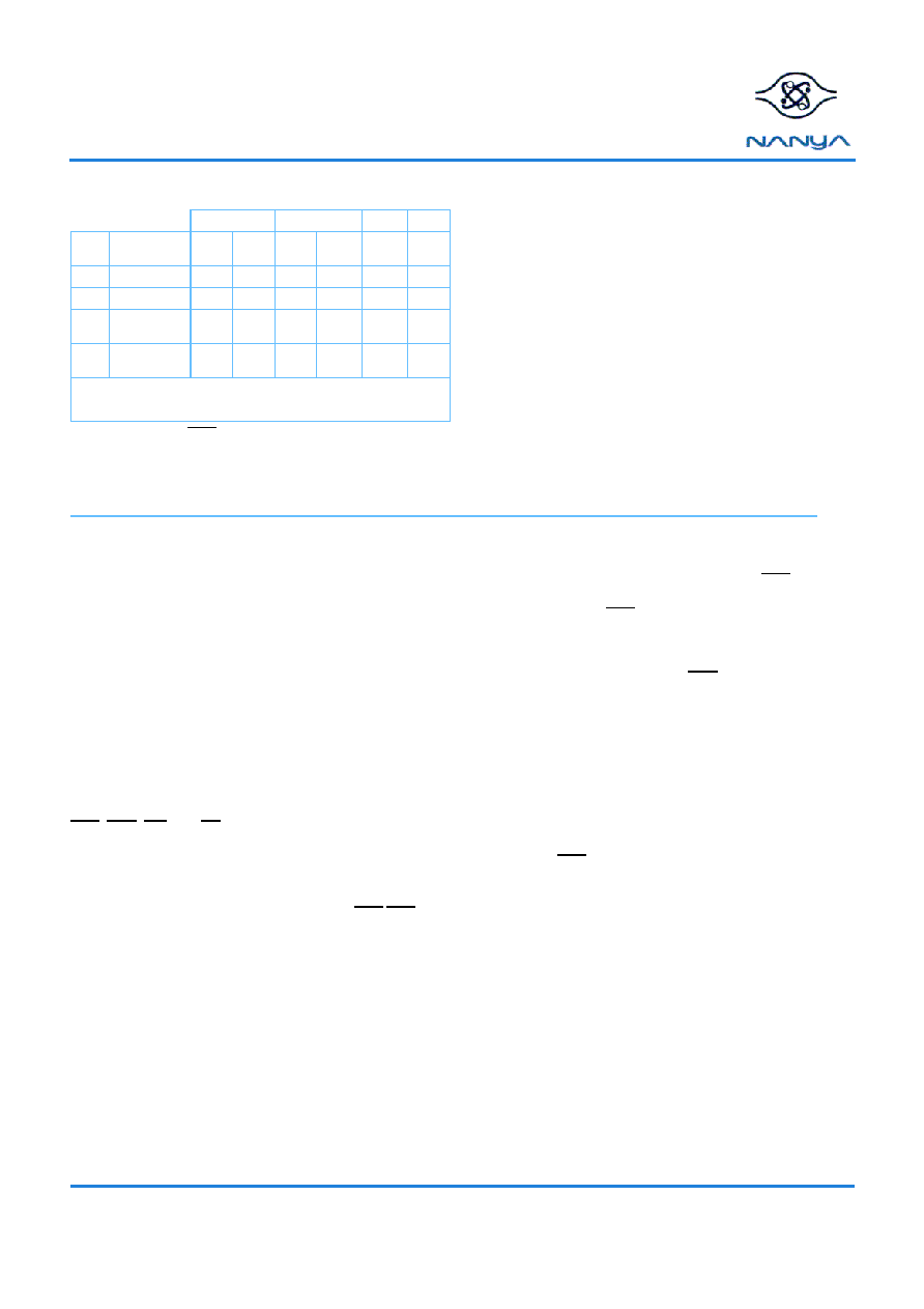
-6K
-7K
-7
Units
f
CK
Clock
Frequency
166
133
143
133
143
MHz
t
CK
Clock Cycle
6
7.5
7
7.5
7
ns
CL CAS Latency CL=3 CL=2 CL=3 CL=2
CL=3
CKs
t
AC
Clock Access
Time
1
---
--
---
--
--
ns
t
AC
Clock Access
Time
2
5.4
5.4
5.4
5.4
5.4
ns
1. Terminated load. See AC Characteristics on page 16.
2. Unterminated load. See AC Characteristics on page 16.

NT5SV16M4DT
NT5SV8M8DT
NT5SV4M16DT
64Mb Synchronous DRAM
REV 1.1
10/01
2
©
NANYA TECHNOLOGY CORP
. All rights reserved.
NANYA TECHNOLOGY CORP. reserves the right to change Products and Specifications without notice.
Pin Assignments for Planar Components
(Top View)
54-pin Plastic TSOP(II) 400 mil
4Mbit x 4 I/O x 4 Bank
NT5SV16M4DT
1
2
3
4
5
6
9
10
11
12
13
14
7
8
15
16
17
18
19
20
21
22
54
53
52
51
50
49
46
45
44
43
42
41
48
47
40
39
38
37
36
35
34
33
V
DD
NC
V
DDQ
NC
DQ0
V
SSQ
V
DDQ
NC
DQ1
V
SSQ
NC
V
DD
NC
NC
NC
WE
CAS
RAS
CS
BS0
BS1
V
SS
NC
V
SSQ
NC
DQ3
V
DDQ
V
SSQ
NC
DQ2
V
DDQ
NC
V
SS
NC
NC
NC
DQM
CK
CKE
NC
A11
A9
23
24
25
32
31
30
A10/AP
A0
A1
A2
A8
A7
A6
A5
26
27
29
28
A3
V
DD
A4
V
SS
V
DD
DQ0
V
DDQ
NC
DQ1
V
SSQ
V
DDQ
NC
DQ3
V
SSQ
NC
V
DD
NC
DQ2
NC
WE
CAS
RAS
CS
BS0
BS1
A10/AP
A0
A1
A2
A3
V
DD
V
SS
DQ7
V
SSQ
NC
DQ6
V
DDQ
V
SSQ
NC
DQ4
V
DDQ
NC
V
SS
NC
DQ5
NC
DQM
CK
CKE
NC
A11
A9
A8
A7
A6
A5
A4
V
SS
V
DD
DQ0
V
DDQ
DQ1
DQ2
V
SSQ
V
DDQ
DQ5
DQ6
V
SSQ
DQ7
V
DD
DQ3
DQ4
LDQM
WE
CAS
RAS
CS
BS0
BS1
A10/AP
A0
A1
A2
A3
V
DD
V
SS
DQ15
V
SSQ
DQ14
DQ13
V
DDQ
V
SSQ
DQ10
DQ9
V
DDQ
DQ8
V
SS
DQ12
DQ11
NC
UDQM
CK
CKE
NC
A11
A9
A8
A7
A6
A5
A4
V
SS
1Mbit x 16 I/O x 4 Bank
NT5SV4M16DT
2Mbit x 8 I/O x 4 Bank
NT5SV8M8DT
NT5SV16M4DT
NT5SV8M8DT
NT5SV4M16DT
64Mb Synchronous DRAM
REV 1.1
10/01
3
©
NANYA TECHNOLOGY CORP
. All rights reserved.
NANYA TECHNOLOGY CORP. reserves the right to change Products and Specifications without notice.
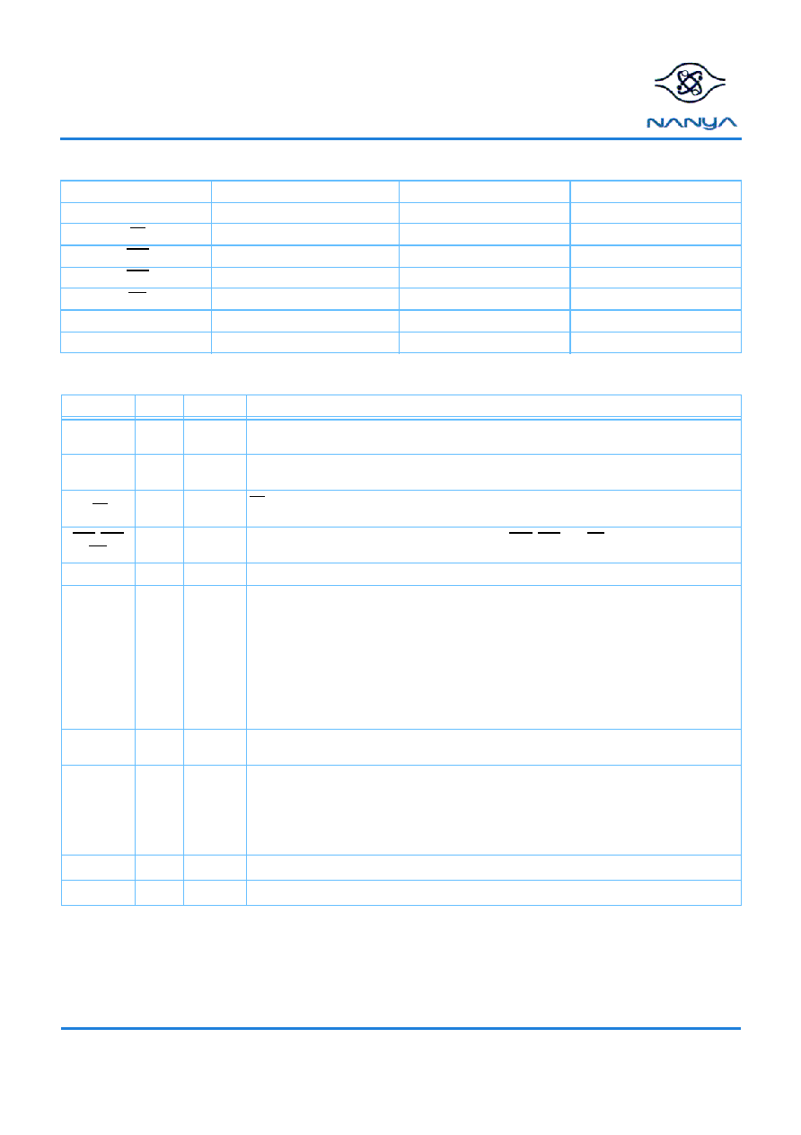
Pin Description
CK
Clock Input
DQ0-DQ15
Data Input/Output
CKE
Clock Enable
DQM, LDQM, UDQM
Data Mask
CS
Chip Select
V
DD
Power (+3.3V)
RAS
Row Address Strobe
V
SS
Ground
CAS
Column Address Strobe
V
DDQ
Power for DQs (+3.3V)
WE
Write Enable
V
SSQ
Ground for DQs
BS1, BS0
Bank Select
NC
No Connection
A0 - A11
Address Inputs
--
--
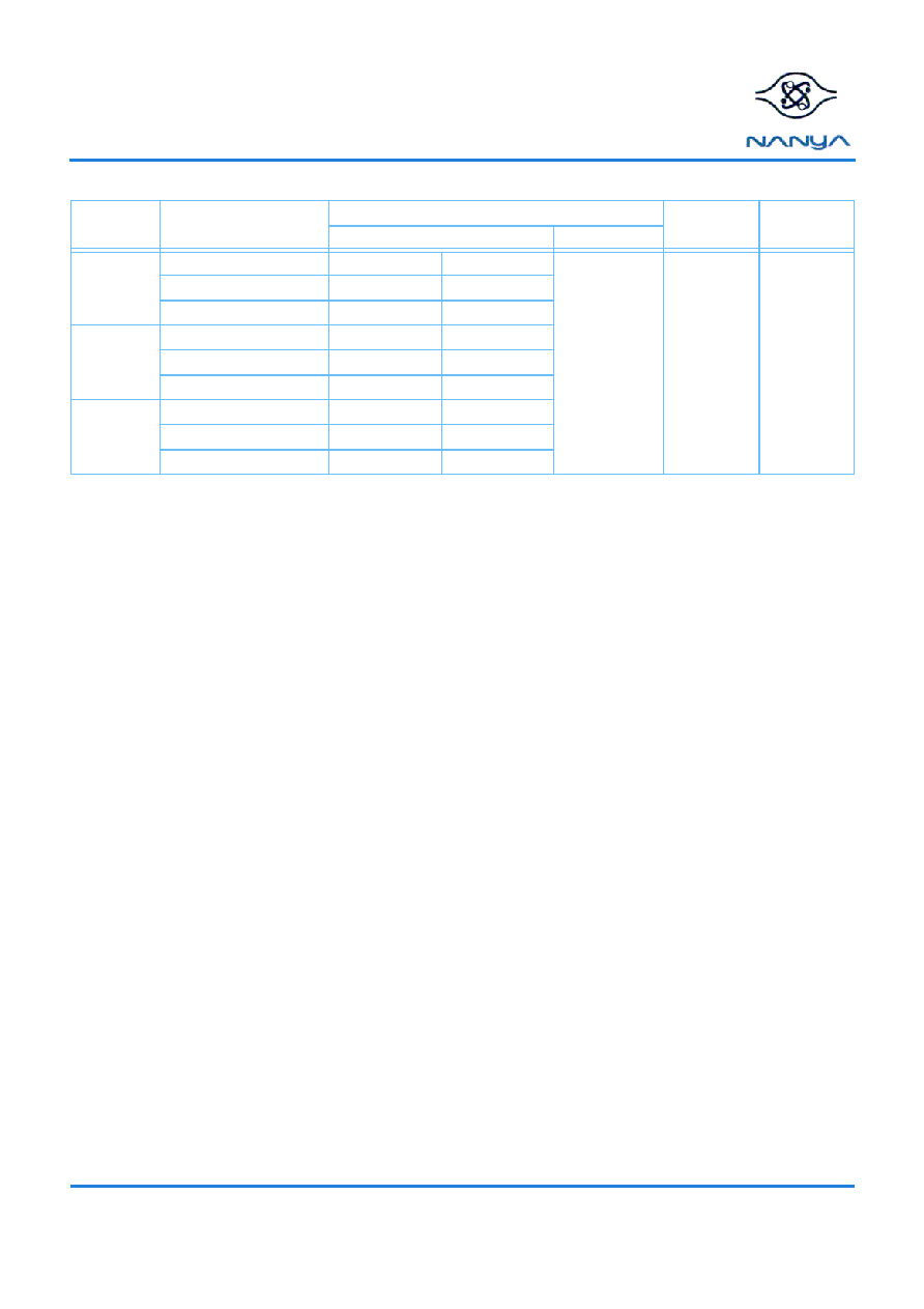
Input/Output Functional Description
Symbol
Type
Polarity
Function
CLK
Input
Positive
Edge
The system clock input. All of the SDRAM inputs are sampled on the rising edge of the clock.
CKE
Input
Active High
Activates the CLK signal when high and deactivates the CLK signal when low. By deactivating the
clock, CKE low initiates the Power Down mode, Suspend mode, or the Self Refresh mode.
CS
Input
Active Low
CS enables the command decoder when low and disables the command decoder when high. When the
command decoder is disabled, new commands are ignored but previous operations continue.
RAS, CAS,
WE
Input
Active Low
When sampled at the positive rising edge of the clock, CAS, RAS, and WE define the operation to be
executed by the SDRAM.
BS0, BS1
Input
--
Selects which bank is to be active.
A0 - A11
Input
--
During a Bank Activate command cycle, A0-A11 defines the row address (RA0-RA11) when sampled at
the rising clock edge.
During a Read or Write command cycle, A0-A9 defines the column address (CA0-CA9) when sampled
at the rising clock edge.
A10 is used to invoke auto-precharge operation at the end of the burst read or write cycle. If A10 is
high, auto-precharge is selected and BS0, BS1 defines the bank to be precharged. If A10 is low, auto-
precharge is disabled.
During a Precharge command cycle, A10 is used in conjunction with BS0, BS1 to control which bank(s)
to precharge. If A10 is high, all banks will be precharged regardless of the state of BS. If A10 is low,
then BS0 and BS1 are used to define which bank to precharge.
DQ0 - DQ15
Input-
Output
--
Data Input/Output pins operate in the same manner as on conventional DRAMs.
DQM
LDQM
UDQM
Input
Active High
The Data Input/Output mask places the DQ buffers in a high impedance state when sampled high. In
x16 products, LDQM and UDQM control the lower and upper byte I/O buffers, respectively. In Read
mode, DQM has a latency of two clock cycles and controls the output buffers like an output enable.
DQM low turns the output buffers on and DQM high turns them off. In Write mode, DQM has a latency
of zero and operates as a word mask by allowing input data to be written if it is low but blocks the write
operation if DQM is high.
V
DD
, V
SS
Supply
--
Power and ground for the input buffers and the core logic.
V
DDQ
V
SSQ
Supply
--
Isolated power supply and ground for the output buffers to provide improved noise immunity.
NT5SV16M4DT
NT5SV8M8DT
NT5SV4M16DT
64Mb Synchronous DRAM
REV 1.1
10/01
4
©
NANYA TECHNOLOGY CORP
. All rights reserved.
NANYA TECHNOLOGY CORP. reserves the right to change Products and Specifications without notice.
Ordering Information
Organization
Part Number
Speed Grade
Power
Supply
Package
Clock Frequency@CAS Latency
Note
16M x 4
NT5SV16M4DT-6K
166MHz@CL3
133MHz@CL2
PC133 , PC100
3.3 V
400mil 54-PIN
TSOP II
NT5SV16M4DT-7K
143MHz@CL3
133MHz@CL2
NT5SV16M4DT-7
143MHz@CL3
100MHz@CL2
8M x 8
NT5SV8M8DT-6K
166MHz@CL3
133MHz@CL2
NT5SV8M8DT-7K
143MHz@CL3
133MHz@CL2
NT5SV8M8DT-7
143MHz@CL3
100MHz@CL2
4M x 16
NT5SV4M16DT
-
6K
166MHz@CL3
133MHz@CL2
NT5SV4M16DT-7K
143MHz@CL3
133MHz@CL2
NT5SV4M16DT-7
143MHz@CL3
100MHz@CL2
NT5SV16M4DT
NT5SV8M8DT
NT5SV4M16DT
64Mb Synchronous DRAM
REV 1.1
10/01
5
©
NANYA TECHNOLOGY CORP
. All rights reserved.
NANYA TECHNOLOGY CORP. reserves the right to change Products and Specifications without notice.
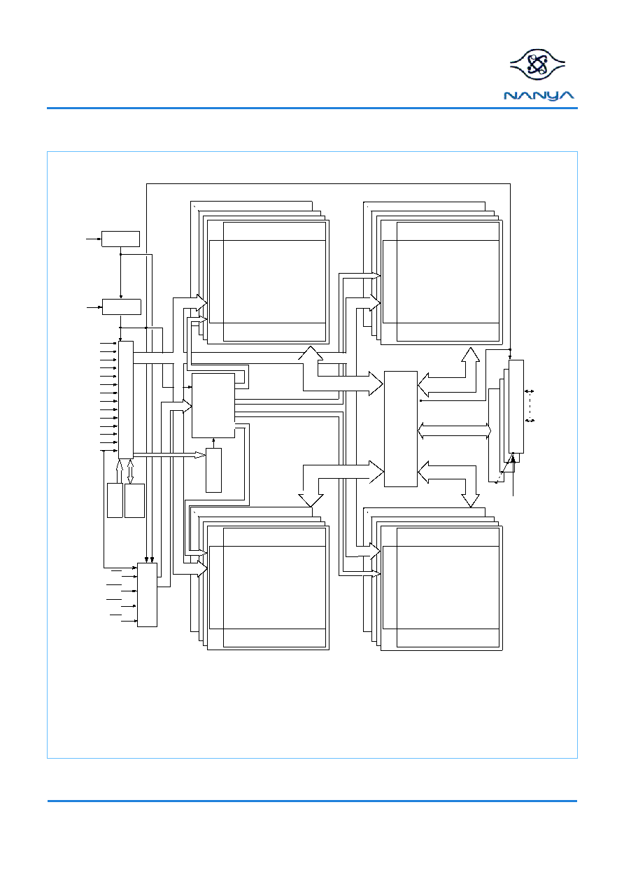
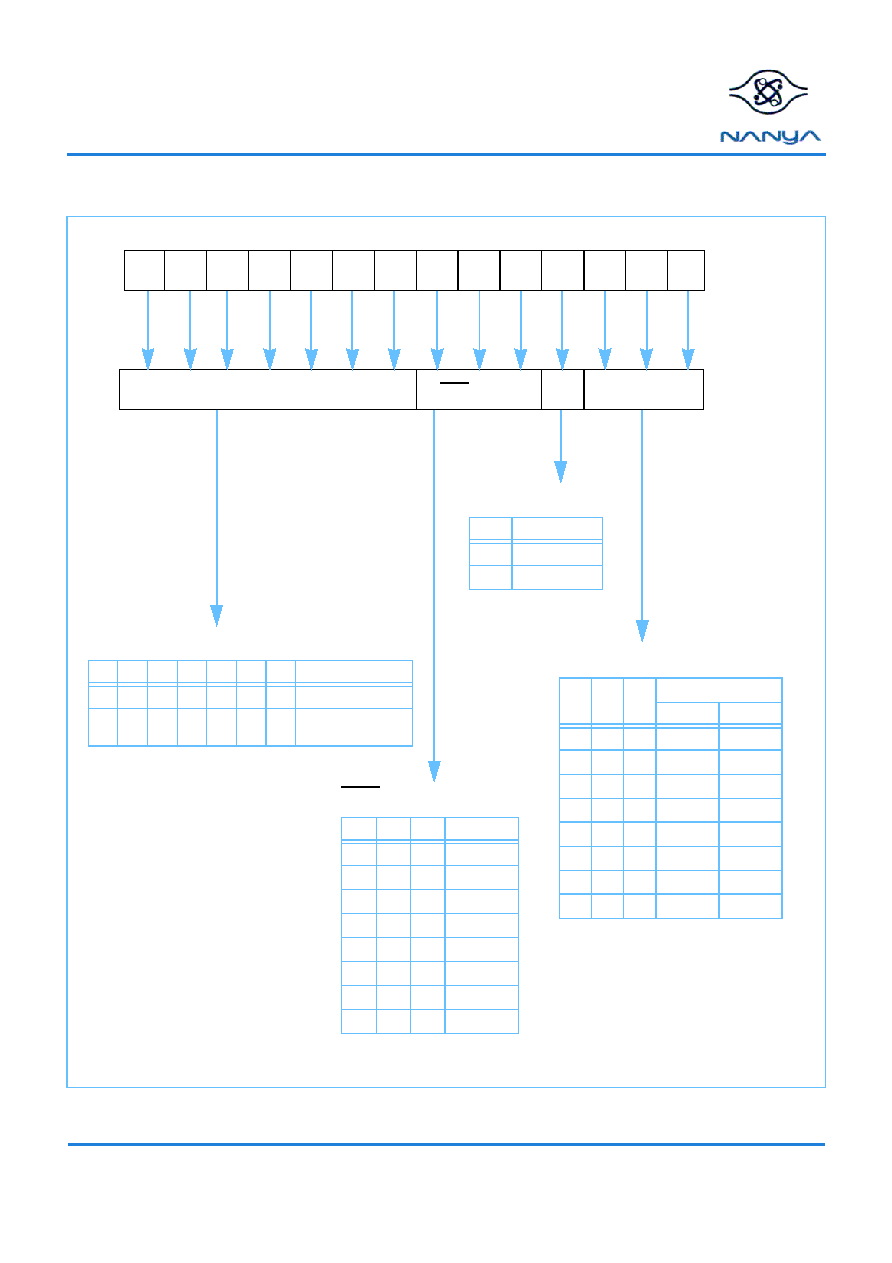
Block Diagram
DQ
0
DQ
X
D
a
t
a
I
n
p
u
t
/
O
u
t
p
u
t
B
u
f
f
e
r
s
CKE Buffer
CLK Buffer
CKE
CLK
CS
RAS
CAS
DQM
WE
C
o
m
m
a
n
d
D
e
c
o
d
e
r
M
o
d
e
R
e
g
i
s
t
e
r
C
o
u
n
t
e
r
C
o
l
u
m
n
A
d
d
r
e
s
s
C
o
u
n
t
e
r
R
e
f
r
e
s
h
A1
A2
A3
A4
A5
A6
A7
A10
A8
A9
A0
A11
Sense Amplifiers
Memory Bank 1
Cell Array
R
o
w
D
e
c
o
d
e
r
A
d
d
r
e
s
s
B
u
f
f
e
r
s
(
1
4
)
Column Decoder
Sense Amplifiers
Memory Bank 3
Cell Array
R
o
w
D
e
c
o
d
e
r
Column Decoder
Sense Amplifiers
Memory Bank 0
Cell Array
R
o
w
D
e
c
o
d
e
r
Column Decoder
Sense Amplifiers
Memory Bank 2
Cell Array
R
o
w
D
e
c
o
d
e
r
Column Decoder
D
a
t
a
C
o
n
t
r
o
l
C
i
r
c
u
i
t
r
y
BS1
BS0
C
o
n
t
r
o
l
S
i
g
n
a
l
G
e
n
e
r
a
t
o
r
Cell Array, per bank, for 4Mb x 4 DQ: 4096 Row x 1024 Col x 4 DQ (DQ0-DQ3).
Cell Array, per bank, for 2Mb x 8 DQ: 4096 Row x 512 Col x 8 DQ (DQ0-DQ7)
.
Cell Array, per bank, for 1Mb x 16 DQ: 4096 Row x 256 Col x 16 DQ (DQ0-DQ15).
NT5SV16M4DT
NT5SV8M8DT
NT5SV4M16DT
64Mb Synchronous DRAM
REV 1.1
10/01
6
©
NANYA TECHNOLOGY CORP
. All rights reserved.
NANYA TECHNOLOGY CORP. reserves the right to change Products and Specifications without notice.
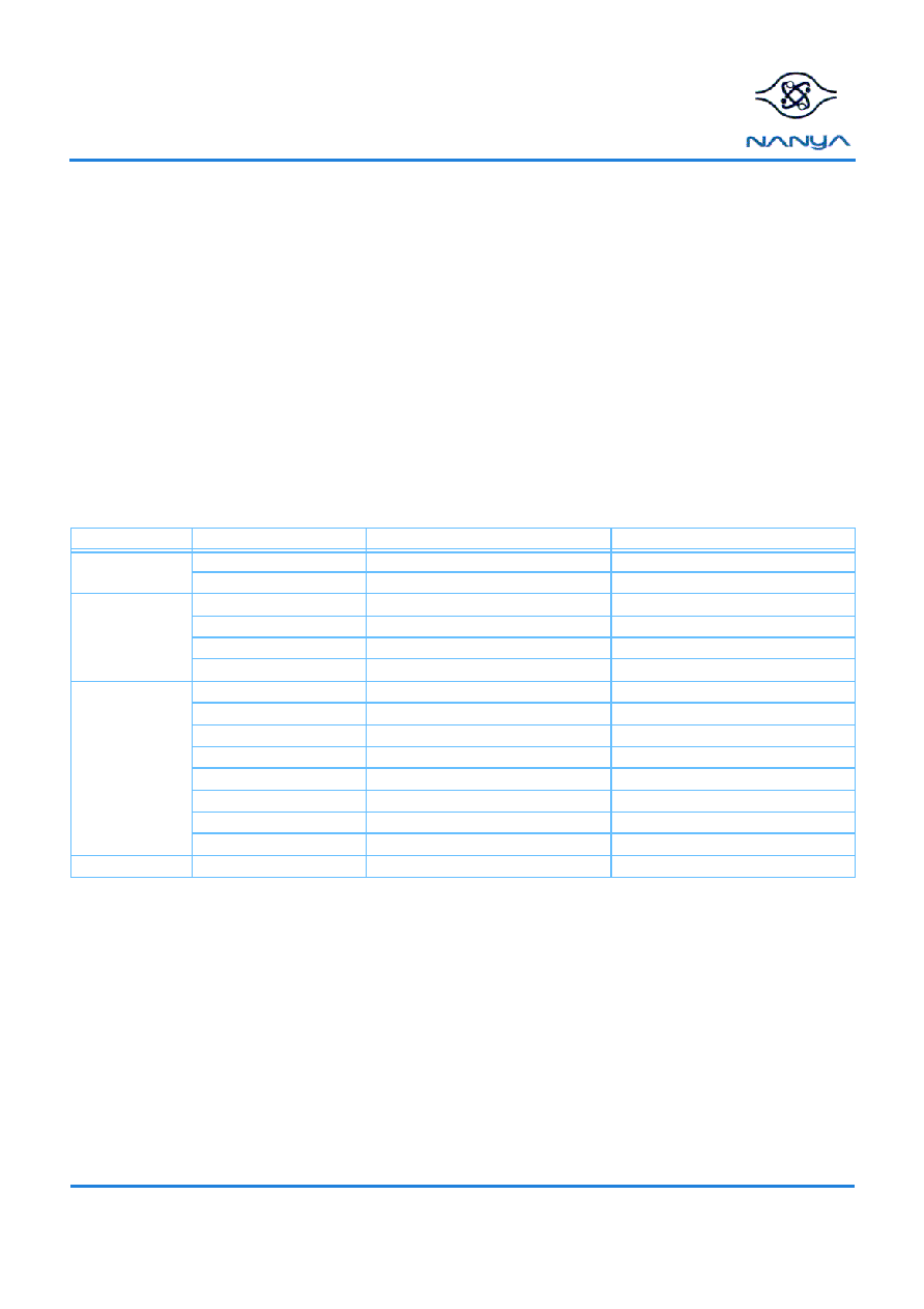
Mode Register Operation (Address Input For Mode Set)
A11
A3
A4
A2
A1
A0
A10
A9
A8
A7
A6
A5
Address
BT
Burst Length
CAS Latency
Mode
CAS Latency
M6
M5
M4
Latency
0
0
0
Reserved
0
0
1
Reserved
0
1
0
2
0
1
1
3
1
0
0
Reserved
1
0
1
Reserved
1
1
0
Reserved
1
1
1
Reserved
Burst Length
M2
M1
M0
Length
Sequential Interleave
0
0
0
1
1
0
0
1
2
2
0
1
0
4
4
0
1
1
8
8
1
0
0
Reserved Reserved
1
0
1
Reserved Reserved
1
1
0
Reserved Reserved
1
1
1
Full Page Reserved
Burst Type
M3
Type
0
Sequential
1
Interleave
Operation Mode
M13 M12 M11 M10 M9 M8 M7
Mode
0
0
0
0
0
0
0
Normal
0
0
0
0
1
0
0
Multiple Burst with
Single Write
Operation Mode
BS1
Bus (Ax)
Register(Mx)
BS0
NT5SV16M4DT
NT5SV8M8DT
NT5SV4M16DT
64Mb Synchronous DRAM
REV 1.1
10/01
7
©
NANYA TECHNOLOGY CORP
. All rights reserved.
NANYA TECHNOLOGY CORP. reserves the right to change Products and Specifications without notice.
Burst Mode Operation
Burst mode operation is used to provide a constant flow of data to memory locations (write cycle), or from memory locations
(read cycle). There are three parameters that define how the burst mode will operate. These parameters include burst
sequence, burst length, and operation mode. The burst sequence and burst length are programmable, and are determined by
address bits A0 - A3 during the Mode Register Set command. Operation mode is also programmable and is set by address bits
A7 - A11, BS0, and BS1.
The burst type is used to define the order in which the burst data will be delivered or stored to the SDRAM. Two types of burst
sequences are supported, sequential and interleaved. See the table below.
The burst length controls the number of bits that will be output after a Read Command, or the number of bits to be input after a
Write Command. The burst length can be programmed to have values of 1, 2, 4, 8 or full page(actual page length is dependent
on organization: x4, x8, or x16).Full page burst operation is only posible using the sequential burst type.
Burst operation mode can be normal operation or multiple burst with single write operation. Normal operation implies that the
device will perform burst operations on both read and write cycles until the desired burst length is satisfied. Multiple burst with
single write operation was added to support Write Through Cache operation. Here, the programmed burst length only applies to
read cycles. All write cycles are single write operations when this mode is selected.
Note: Page length is a function of I/O organization and column addressing.
x4 organization (CA0-CA9); Page Length = 1024 bits
x8 organization (CA0-CA8); Page Length = 512 bits
x16 organization (CA0-CA7); Page Length = 256 bits
Burst Length and Sequence
Burst Length
Starting Address (A2 A1 A0)
Sequential Addressing (decimal)
Interleave Addressing (decimal)
2
x x 0
0, 1
0, 1
x x 1
1, 0
1, 0
4
x 0 0
0, 1, 2, 3
0, 1, 2, 3
x 0 1
1, 2, 3, 0
1, 0, 3, 2
x 1 0
2, 3, 0, 1
2, 3, 0, 1
x 1 1
3, 0, 1, 2
3, 2, 1, 0
8
0 0 0
0, 1, 2, 3, 4, 5, 6, 7
0, 1, 2, 3, 4, 5, 6, 7
0 0 1
1, 2, 3, 4, 5, 6, 7, 0
1, 0, 3, 2, 5, 4, 7, 6
0 1 0
2, 3, 4, 5, 6, 7, 0, 1
2, 3, 0, 1, 6, 7, 4, 5
0 1 1
3, 4, 5, 6, 7, 0, 1, 2
3, 2, 1, 0, 7, 6, 5, 4
1 0 0
4, 5, 6, 7, 0, 1, 2, 3
4, 5, 6, 7, 0, 1, 2, 3
1 0 1
5, 6, 7, 0, 1, 2, 3, 4
5, 4, 7, 6, 1, 0, 3, 2
1 1 0
6, 7, 0, 1, 2, 3, 4, 5
6, 7, 4, 5, 2, 3, 0, 1
1 1 1
7, 0, 1, 2, 3, 4, 5, 6
7, 6, 5, 4, 3, 2, 1, 0
Full Page(Note)
n n n
Cn, Cn+1, Cn+2, .....
Not Supported
NT5SV16M4DT
NT5SV8M8DT
NT5SV4M16DT
64Mb Synchronous DRAM
REV 1.1
10/01
8
©
NANYA TECHNOLOGY CORP
. All rights reserved.
NANYA TECHNOLOGY CORP. reserves the right to change Products and Specifications without notice.
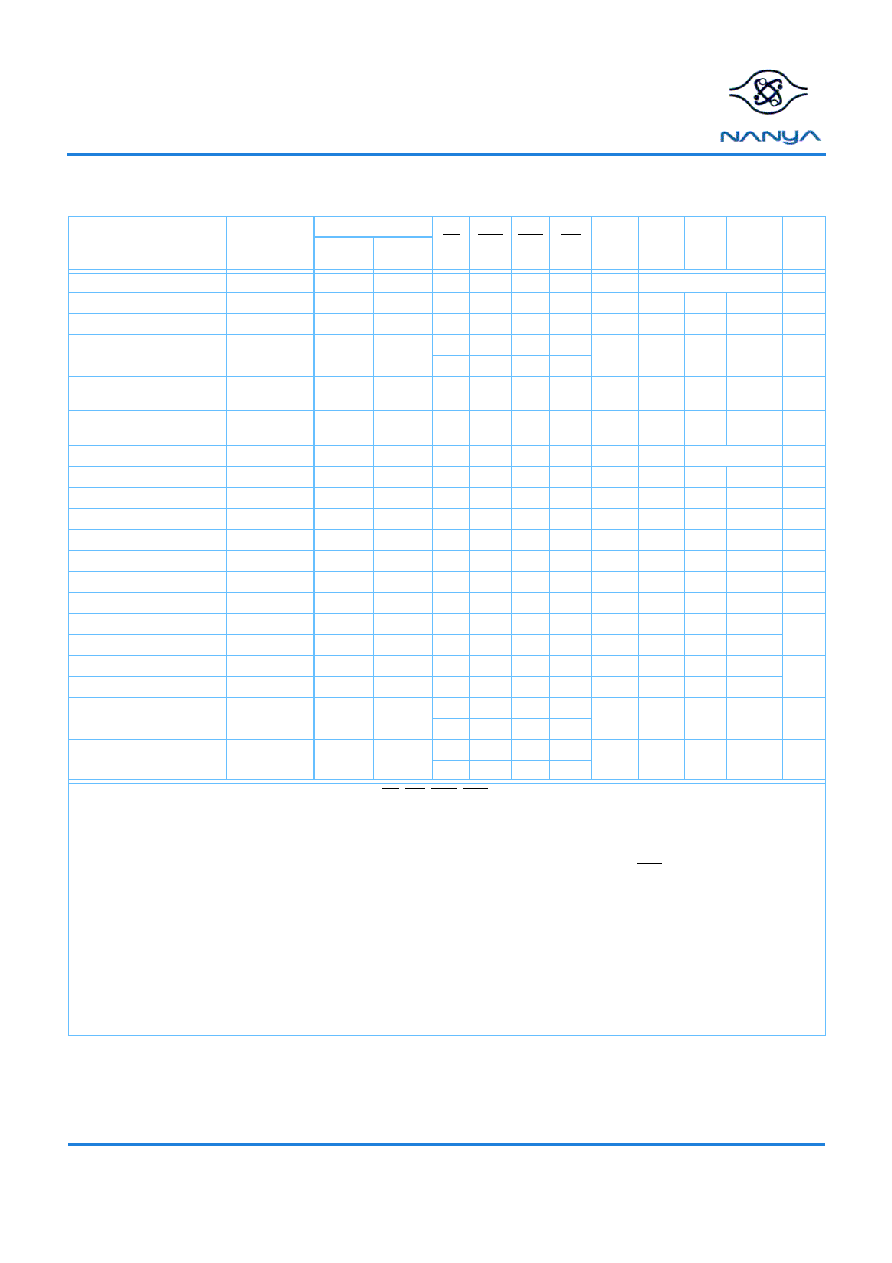
Command Truth Table
(See note 1)
Function
Device State
CKE
CS
RAS
CAS
WE
DQM
BS0,
BS1
A10
A11,
A11,
A9-A0
Notes
Previous
Cycle
Current
Cycle
Mode Register Set
Idle
H
X
L
L
L
L
X
OP Code
Auto (CBR) Refresh
Idle
H
H
L
L
L
H
X
X
X
X
Entry Self Refresh
Idle
H
L
L
L
L
H
X
X
X
X
Exit Self Refresh
Idle (Self-
Refresh)
L
H
H
X
X
X
X
X
X
X
L
H
H
H
Single Bank Precharge
See Current
State Table
H
X
L
L
H
L
X
BS
L
X
2
Precharge all Banks
See Current
State Table
H
X
L
L
H
L
X
X
H
X
Bank Activate
Idle
H
X
L
L
H
H
X
BS
Row Address
2
Write
Active
H
X
L
H
L
L
X
BS
L
Column
2
Write with Auto-Precharge
Active
H
X
L
H
L
L
X
BS
H
Column
2
Read
Active
H
X
L
H
L
H
X
BS
L
Column
2
Read with Auto-Precharge
Active
H
X
L
H
L
H
X
BS
H
Column
2
Burst Termination
Active
H
X
L
H
H
L
X
X
X
X
3,8
No Operation
Any
H
X
L
H
H
H
X
X
X
X
Device Deselect
Any
H
X
H
X
X
X
X
X
X
X
Clock Suspend Mode Entry Active
H
L
X
X
X
X
X
X
X
X
4
Clock Suspend Mode Exit
Active
L
H
X
X
X
X
X
X
X
X
Data Write/Output Enable
Active
H
X
X
X
X
X
L
X
X
X
5
Data Mask/Output Disable
Active
H
X
X
X
X
X
H
X
X
X
Power Down Mode Entry
Idle/Active
H
L
H
X
X
X
X
X
X
X
6, 7
L
H
H
H
Power Down Mode Exit
Any (Power
Down)
L
H
H
X
X
X
X
X
X
X
6, 7
L
H
H
H
1. All of the SDRAM operations are defined by states of CS, WE, RAS, CAS, and DQM at the positive rising edge of the clock.Operation of
both decks of a stacked device at the same time is allowed, depending on the operation being performed on the other deck. Refer to the
Current State Truth Table.
2. Bank Select (BS0, BS1): BS0, BS1 = 0,0 selects bank 0; BS0, BS1 = 1,0 selects bank 1; BS0, BS1 = 0,1 selects bank 2; BS0, BS1 = 1,1
selects bank 3.
3. During a Burst Write cycle there is a zero clock delay; for a Burst Read cycle the delay is equal to the CAS latency.
4. During normal access mode, CKE is held high and CK is enabled. When it is low, it freezes the internal clock and extends data Read and
Write operations. One clock delay is required for mode entry and exit.
5. The DQM has two functions for the data DQ Read and Write operations. During a Read cycle, when DQM goes high at a clock timing the
data outputs are disabled and become high impedance after a two-clock delay. DQM also provides a data mask function for Write cycles.
When it activates, the Write operation at the clock is prohibited (zero clock latency).
6. All banks must be precharged before entering the Power Down Mode. (If this command is issued during a burst operation, the device
state will be Clock Suspend Mode.) The Power Down Mode does not perform any refresh operations; therefore the device can't remain in
this mode longer than the Refresh period (t
REF
) of the device. One clock delay is required for mode entry and exit.
7. A No Operation or Device Deselect Command is required on the next clock edge following CKE going high.
8. Device state is full page burst operation. Use of this command to terminate other burst length operations is illegal.
NT5SV16M4DT
NT5SV8M8DT
NT5SV4M16DT
64Mb Synchronous DRAM
REV 1.1
10/01
9
©
NANYA TECHNOLOGY CORP
. All rights reserved.
NANYA TECHNOLOGY CORP. reserves the right to change Products and Specifications without notice.
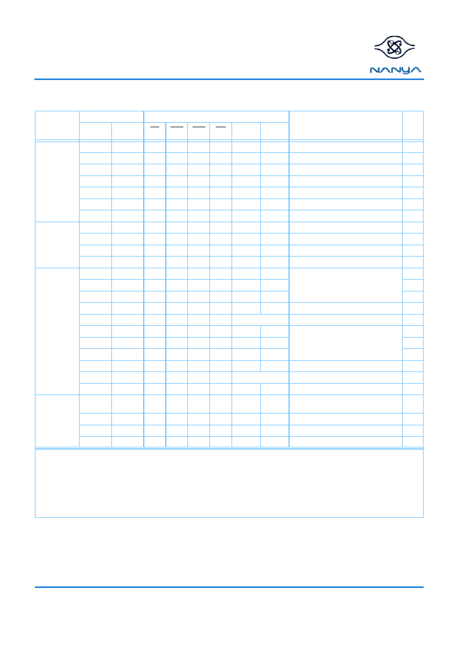
Clock Enable (CKE) Truth Table
Current State
CKE
Command
Action
Notes
Previous
Cycle
Current
Cycle
CS
RAS
CAS
WE
BS0,
BS1
A11 - A0
Self Refresh
H
X
X
X
X
X
X
X
INVALID
1
L
H
H
X
X
X
X
X
Exit Self Refresh with Device Deselect
2
L
H
L
H
H
H
X
X
Exit Self Refresh with No Operation
2
L
H
L
H
H
L
X
X
ILLEGAL
2
L
H
L
H
L
X
X
X
ILLEGAL
2
L
H
L
L
X
X
X
X
ILLEGAL
2
L
L
X
X
X
X
X
X
Maintain Self Refresh
Power Down
H
X
X
X
X
X
X
X
INVALID
1
L
H
H
X
X
X
X
X
Power Down mode exit, all banks idle
2
L
H
L
X
X
X
X
X
ILLEGAL
2
L
L
X
X
X
X
X
X
Maintain Power Down Mode
All Banks Idle
H
H
H
X
X
X
Refer to the Idle State section of the
Current State Truth Table
3
H
H
L
H
X
X
3
H
H
L
L
H
X
3
H
H
L
L
L
H
X
X
CBR Refresh
H
H
L
L
L
L
OP Code
Mode Register Set
4
H
L
H
X
X
X
Refer to the Idle State section of the
Current State Truth Table
3
H
L
L
H
X
X
3
H
L
L
L
H
X
3
H
L
L
L
L
H
X
X
Entry Self Refresh
4
H
L
L
L
L
L
OP Code
Mode Register Set
L
X
X
X
X
X
X
X
Power Down
4
Any State
other than
listed above
H
H
X
X
X
X
X
X
Refer to operations in the Current State
Truth Table
H
L
X
X
X
X
X
X
Begin Clock Suspend next cycle
5
L
H
X
X
X
X
X
X
Exit Clock Suspend next cycle
L
L
X
X
X
X
X
X
Maintain Clock Suspend
1. For the given Current State CKE must be low in the previous cycle.
2. When CKE has a low to high transition, the clock and other inputs are re-enabled asynchronously. The minimum setup time for CKE
(t
CES
) must be satisfied. When exiting power down mode, a NOP command (or Device Deselect Command) is required on the first rising
clock after CKE goes high (see page 26).
3. The address inputs depend on the command that is issued. See the Idle State section of the Current State Truth Table for more informa-
tion.
4. The Precharge Power Down Mode, the Self Refresh Mode, and the Mode Register Set can only be entered from the all banks idle state.
5. Must be a legal command as defined in the Current State Truth Table.
NT5SV16M4DT
NT5SV8M8DT
NT5SV4M16DT
64Mb Synchronous DRAM
REV 1.1
10/01
10
©
NANYA TECHNOLOGY CORP
. All rights reserved.
NANYA TECHNOLOGY CORP. reserves the right to change Products and Specifications without notice.
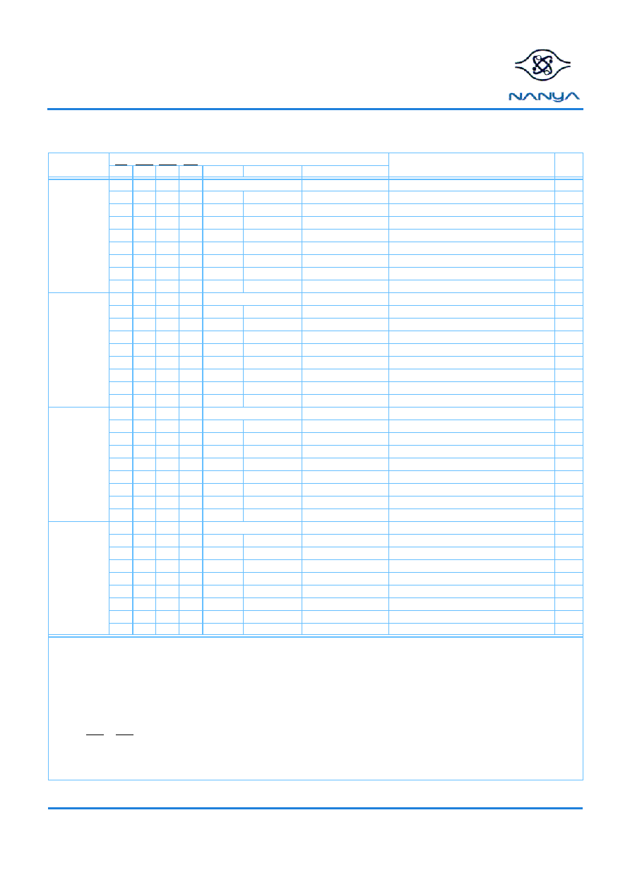
Current State Truth Table
(Part 1 of 3)(See note 1)
Current State
Command
Action
Notes
CS RAS CAS WE BS0,BS1
A11 - A0
Description
Idle
L
L
L
L
OP Code
Mode Register Set
Set the Mode Register
2
L
L
L
H
X
X
Auto or Self Refresh
Start Auto or Self Refresh
2, 3
L
L
H
L
BS
X
Precharge
No Operation
L
L
H
H
BS
Row Address Bank Activate
Activate the specified bank and row
L
H
L
L
BS
Column
Write w/o Precharge
ILLEGAL
4
L
H
L
H
BS
Column
Read w/o Precharge
ILLEGAL
4
L
H
H
L
X
X
Burst Termination
No Operation
L
H
H
H
X
X
No Operation
No Operation
H
X
X
X
X
X
Device Deselect
No Operation or Power Down
5
Row Active
L
L
L
L
OP Code
Mode Register Set
ILLEGAL
L
L
L
H
X
X
Auto or Self Refresh
ILLEGAL
L
L
H
L
BS
X
Precharge
Precharge
6
L
L
H
H
BS
Row Address Bank Activate
ILLEGAL
4
L
H
L
L
BS
Column
Write
Start Write; Determine if Auto Precharge
7, 8
L
H
L
H
BS
Column
Read
Start Read; Determine if Auto Precharge
7, 8
L
H
H
L
X
X
Burst Termination
No Operation
L
H
H
H
X
X
No Operation
No Operation
H
X
X
X
X
X
Device Deselect
No Operation
Read
L
L
L
L
OP Code
Mode Register Set
ILLEGAL
L
L
L
H
X
X
Auto or Self Refresh
ILLEGAL
L
L
H
L
BS
X
Precharge
Terminate Burst; Start the Precharge
L
L
H
H
BS
Row Address Bank Activate
ILLEGAL
4
L
H
L
L
BS
Column
Write
Terminate Burst; Start the Write cycle
8, 9
L
H
L
H
BS
Column
Read
Terminate Burst; Start a new Read cycle
8, 9
L
H
H
L
X
X
Burst Termination
Terminate the Burst
L
H
H
H
X
X
No Operation
Continue the Burst
H
X
X
X
X
X
Device Deselect
Continue the Burst
Write
L
L
L
L
OP Code
Mode Register Set
ILLEGAL
L
L
L
H
X
X
Auto or Self Refresh
ILLEGAL
L
L
H
L
BS
X
Precharge
Terminate Burst; Start the Precharge
L
L
H
H
BS
Row Address Bank Activate
ILLEGAL
4
L
H
L
L
BS
Column
Write
Terminate Burst; Start a new Write cycle
8, 9
L
H
L
H
BS
Column
Read
Terminate Burst; Start the Read cycle
8, 9
L
H
H
L
X
X
Burst Termination
Terminate the Burst
L
H
H
H
X
X
No Operation
Continue the Burst
H
X
X
X
X
X
Device Deselect
Continue the Burst
1. CKE is assumed to be active (high) in the previous cycle for all entries. The Current State is the state of the bank that the Command is
being applied to.
2. All Banks must be idle; otherwise, it is an illegal action.
3. If CKE is active (high) the SDRAM will start the Auto (CBR) Refresh operation, if CKE is inactive (low) than the Self Refresh mode is
entered.
4. The Current State refers to only one of the banks. If BS selects this bank then the action is illegal. If BS selects the bank not being refer-
enced by the Current State then the action may be legal depending on the state of that bank.
5. If CKE is inactive (low) then the Power Down mode is entered; otherwise there is a No Operation.
6. The minimum and maximum Active time (t
RAS
) must be satisfied.
7. The RAS to CAS Delay (t
RCD
) must occur before the command is given.
8. Column address A10 is used to determine if the Auto Precharge function is activated.
9. The command must satisfy any bus contention, bus turn around, and/or write recovery requirements.
10. The command is illegal if the minimum bank to bank delay time (t
RRD
) is not satisfied.

NT5SV16M4DT
NT5SV8M8DT
NT5SV4M16DT
64Mb Synchronous DRAM
REV 1.1
10/01
11
©
NANYA TECHNOLOGY CORP
. All rights reserved.
NANYA TECHNOLOGY CORP. reserves the right to change Products and Specifications without notice.
Read with
Auto Pre-
charge
L
L
L
L
OP Code
Mode Register Set
ILLEGAL
L
L
L
H
X
X
Auto or Self Refresh
ILLEGAL
L
L
H
L
BS
X
Precharge
ILLEGAL
4
L
L
H
H
BS
Row Address Bank Activate
ILLEGAL
4
L
H
L
L
BS
Column
Write
ILLEGAL
4
L
H
L
H
BS
Column
Read
ILLEGAL
4
L
H
H
L
X
X
Burst Termination
ILLEGAL
L
H
H
H
X
X
No Operation
Continue the Burst
H
X
X
X
X
X
Device Deselect
Continue the Burst
Write with Auto
Precharge
L
L
L
L
OP Code
Mode Register Set
ILLEGAL
L
L
L
H
X
X
Auto or Self Refresh
ILLEGAL
L
L
H
L
BS
X
Precharge
ILLEGAL
4
L
L
H
H
BS
Row Address Bank Activate
ILLEGAL
4
L
H
L
L
BS
Column
Write
ILLEGAL
4
L
H
L
H
BS
Column
Read
ILLEGAL
4
L
H
H
L
X
X
Burst Termination
ILLEGAL
L
H
H
H
X
X
No Operation
Continue the Burst
H
X
X
X
X
X
Device Deselect
Continue the Burst
Precharging
L
L
L
L
OP Code
Mode Register Set
ILLEGAL
L
L
L
H
X
X
Auto or Self Refresh
ILLEGAL
L
L
H
L
BS
X
Precharge
No Operation; Bank(s) idle after t
RP
L
L
H
H
BS
Row Address Bank Activate
ILLEGAL
4
L
H
L
L
BS
Column
Write
ILLEGAL
4
L
H
L
H
BS
Column
Read
ILLEGAL
4
L
H
H
L
X
X
Burst Termination
No Operation; Bank(s) idle after t
RP
L
H
H
H
X
X
No Operation
No Operation; Bank(s) idle after t
RP
H
X
X
X
X
X
Device Deselect
No Operation; Bank(s) idle after t
RP
Row
Activating
L
L
L
L
OP Code
Mode Register Set
ILLEGAL
L
L
L
H
X
X
Auto or Self Refresh
ILLEGAL
L
L
H
L
BS
X
Precharge
ILLEGAL
4
L
L
H
H
BS
Row Address Bank Activate
ILLEGAL
4, 10
L
H
L
L
BS
Column
Write
ILLEGAL
4
L
H
L
H
BS
Column
Read
ILLEGAL
4
L
H
H
L
X
X
Burst Termination
No Operation; Row Active after t
RCD
L
H
H
H
X
X
No Operation
No Operation; Row Active after t
RCD
H
X
X
X
X
X
Device Deselect
No Operation; Row Active after t
RCD
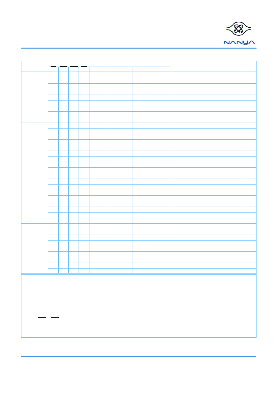
Current State Truth Table
(Part 2 of 3)(See note 1)
Current State
Command
Action
Notes
CS RAS CAS WE BS0,BS1
A11 - A0
Description
1. CKE is assumed to be active (high) in the previous cycle for all entries. The Current State is the state of the bank that the Command is
being applied to.
2. All Banks must be idle; otherwise, it is an illegal action.
3. If CKE is active (high) the SDRAM will start the Auto (CBR) Refresh operation, if CKE is inactive (low) than the Self Refresh mode is
entered.
4. The Current State refers to only one of the banks. If BS selects this bank then the action is illegal. If BS selects the bank not being refer-
enced by the Current State then the action may be legal depending on the state of that bank.
5. If CKE is inactive (low) then the Power Down mode is entered; otherwise there is a No Operation.
6. The minimum and maximum Active time (t
RAS
) must be satisfied.
7. The RAS to CAS Delay (t
RCD
) must occur before the command is given.
8. Column address A10 is used to determine if the Auto Precharge function is activated.
9. The command must satisfy any bus contention, bus turn around, and/or write recovery requirements.
10. The command is illegal if the minimum bank to bank delay time (t
RRD
) is not satisfied.
NT5SV16M4DT
NT5SV8M8DT
NT5SV4M16DT
64Mb Synchronous DRAM
REV 1.1
10/01
12
©
NANYA TECHNOLOGY CORP
. All rights reserved.
NANYA TECHNOLOGY CORP. reserves the right to change Products and Specifications without notice.
Write
Recovering
L
L
L
L
OP Code
Mode Register Set
ILLEGAL
L
L
L
H
X
X
Auto or Self Refresh
ILLEGAL
L
L
H
L
BS
X
Precharge
ILLEGAL
4
L
L
H
H
BS
Row Address Bank Activate
ILLEGAL
4
L
H
L
L
BS
Column
Write
Start Write; Determine if Auto Precharge
9
L
H
L
H
BS
Column
Read
Start Read; Determine if Auto Precharge
9
L
H
H
L
X
X
Burst Termination
No Operation; Row Active after t
DPL
L
H
H
H
X
X
No Operation
No Operation; Row Active after t
DPL
H
X
X
X
X
X
Device Deselect
No Operation; Row Active after t
DPL
Write
Recovering
with
Auto Pre-
charge
L
L
L
L
OP Code
Mode Register Set
ILLEGAL
L
L
L
H
X
X
Auto or Self Refresh
ILLEGAL
L
L
H
L
BS
X
Precharge
ILLEGAL
4
L
L
H
H
BS
Row Address Bank Activate
ILLEGAL
4
L
H
L
L
BS
Column
Write
ILLEGAL
4, 9
L
H
L
H
BS
Column
Read
ILLEGAL
4, 9
L
H
H
L
X
X
Burst Termination
No Operation; Precharge after t
DPL
L
H
H
H
X
X
No Operation
No Operation; Precharge after t
DPL
H
X
X
X
X
X
Device Deselect
No Operation; Precharge after t
DPL
Refreshing
L
L
L
L
OP Code
Mode Register Set
ILLEGAL
L
L
L
H
X
X
Auto or Self Refresh
ILLEGAL
L
L
H
L
BS
X
Precharge
ILLEGAL
L
L
H
H
BS
Row Address Bank Activate
ILLEGAL
L
H
L
L
BS
Column
Write
ILLEGAL
L
H
L
H
BS
Column
Read
ILLEGAL
L
H
H
L
X
X
Burst Termination
No Operation; Idle after t
RC
L
H
H
H
X
X
No Operation
No Operation; Idle after t
RC
H
X
X
X
X
X
Device Deselect
No Operation; Idle after t
RC
Mode
Register
Accessing
L
L
L
L
OP Code
Mode Register Set
ILLEGAL
L
L
L
H
X
X
Auto or Self Refresh
ILLEGAL
L
L
H
L
BS
X
Precharge
ILLEGAL
L
L
H
H
BS
Row Address Bank Activate
ILLEGAL
L
H
L
L
BS
Column
Write
ILLEGAL
L
H
L
H
BS
Column
Read
ILLEGAL
L
H
H
L
X
X
Burst Termination
ILLEGAL
L
H
H
H
X
X
No Operation
No Operation; Idle after two clock cycles
H
X
X
X
X
X
Device Deselect
No Operation; Idle after two clock cycles
Current State Truth Table
(Part 3 of 3)(See note 1)
Current State
Command
Action
Notes
CS RAS CAS WE BS0,BS1
A11 - A0
Description
1. CKE is assumed to be active (high) in the previous cycle for all entries. The Current State is the state of the bank that the Command is
being applied to.
2. All Banks must be idle; otherwise, it is an illegal action.
3. If CKE is active (high) the SDRAM will start the Auto (CBR) Refresh operation, if CKE is inactive (low) than the Self Refresh mode is
entered.
4. The Current State refers to only one of the banks. If BS selects this bank then the action is illegal. If BS selects the bank not being refer-
enced by the Current State then the action may be legal depending on the state of that bank.
5. If CKE is inactive (low) then the Power Down mode is entered; otherwise there is a No Operation.
6. The minimum and maximum Active time (t
RAS
) must be satisfied.
7. The RAS to CAS Delay (t
RCD
) must occur before the command is given.
8. Column address A10 is used to determine if the Auto Precharge function is activated.
9. The command must satisfy any bus contention, bus turn around, and/or write recovery requirements.
10. The command is illegal if the minimum bank to bank delay time (t
RRD
) is not satisfied.
NT5SV16M4DT
NT5SV8M8DT
NT5SV4M16DT
64Mb Synchronous DRAM
REV 1.1
10/01
13
©
NANYA TECHNOLOGY CORP
. All rights reserved.
NANYA TECHNOLOGY CORP. reserves the right to change Products and Specifications without notice.
Absolute Maximum Ratings
Symbol
Parameter
Rating
Units
Notes
V
DD
Power Supply Voltage
-0.3 to +4.6
V
1
V
DDQ
Power Supply Voltage for Output
-0.3 to +4.6
V
1
V
IN
Input Voltage
-0.3 to V
DD
+0.3
V
1
V
OUT
Output Voltage
-0.3 to V
DD
+0.3
V
1
T
A
Operating Temperature (ambient)
0 to +70
∞
C
1
T
STG
Storage Temperature
-55 to +125
∞
C
1
P
D
Power Dissipation
1.0
W
1
I
OUT
Short Circuit Output Current
50
mA
1
1. Stresses greater than those listed under "Absolute Maximum Ratings" may cause permanent damage to the device. This is a stress rating
only and functional operation of the device at these or any other conditions above those indicated in the operational sections of this spec-
ification is not implied. Exposure to absolute maximum rating conditions for extended periods may affect reliability.
Recommended DC Operating Conditions
(T
A
=
0
∞
C to 70
∞
C)
Symbol
Parameter
Rating
Units
Notes
Min.
Typ.
Max.
V
DD
Supply Voltage
3.0
3.3
3.6
V
1
V
DDQ
Supply Voltage for Output
3.0
3.3
3.6
V
1
V
IH
Input High Voltage
2.0
--
V
DD
+ 0.3
V
1, 2
V
IL
Input Low Voltage
-0.3
--
0.8
V
1, 3
1. All voltages referenced to V
SS
and V
SSQ
.
2. V
IH
(max) = V
DD
+ 1.2V for pulse width
5ns.
3. V
IL
(min) = V
SS
- 1.2V for pulse width
5ns.
Capacitance
(T
A
= 25
∞
C, f = 1MHz, V
DD
= 3.3V
±
0.3V)
Symbol
Parameter
Min.
Typ
Max.
Units
C
I
Input Capacitance (A0-A11, BS0, BS1, CS, RAS, CAS, WE, CKE, DQM)
2.5
3.0
3.8
pF
Input Capacitance (CK)
2.5
2.8
3.5
pF
C
O
Output Capacitance (DQ0 - DQ15)
4.0
4.5
6.5
pF

NT5SV16M4DT
NT5SV8M8DT
NT5SV4M16DT
64Mb Synchronous DRAM
REV 1.1
10/01
14
©
NANYA TECHNOLOGY CORP
. All rights reserved.
NANYA TECHNOLOGY CORP. reserves the right to change Products and Specifications without notice.
DC Electrical Characteristics
(T
A
= 0 to +70
∞
C, V
DD
= 3.3V
±
0.3V)
Symbol
Parameter
Min.
Max.
Units
I
I(L)
Input Leakage Current, any input
(0.0V
V
IN
V
DD
), All Other Pins Not Under Test = 0V
-1
+1
µ
A
I
O(L)
Output Leakage Current
(D
OUT
is disabled, 0.0V
V
OUT
V
DDQ
)
-1
+1
µ
A
V
OH
Output Level (LVTTL)
Output "H" Level Voltage (
IOUT
= -2.0mA)
2.4
--
V
V
OL
Output Level (LVTTL)
Output "L" Level Voltage (I
OUT
= +2.0mA)
--
0.4
V
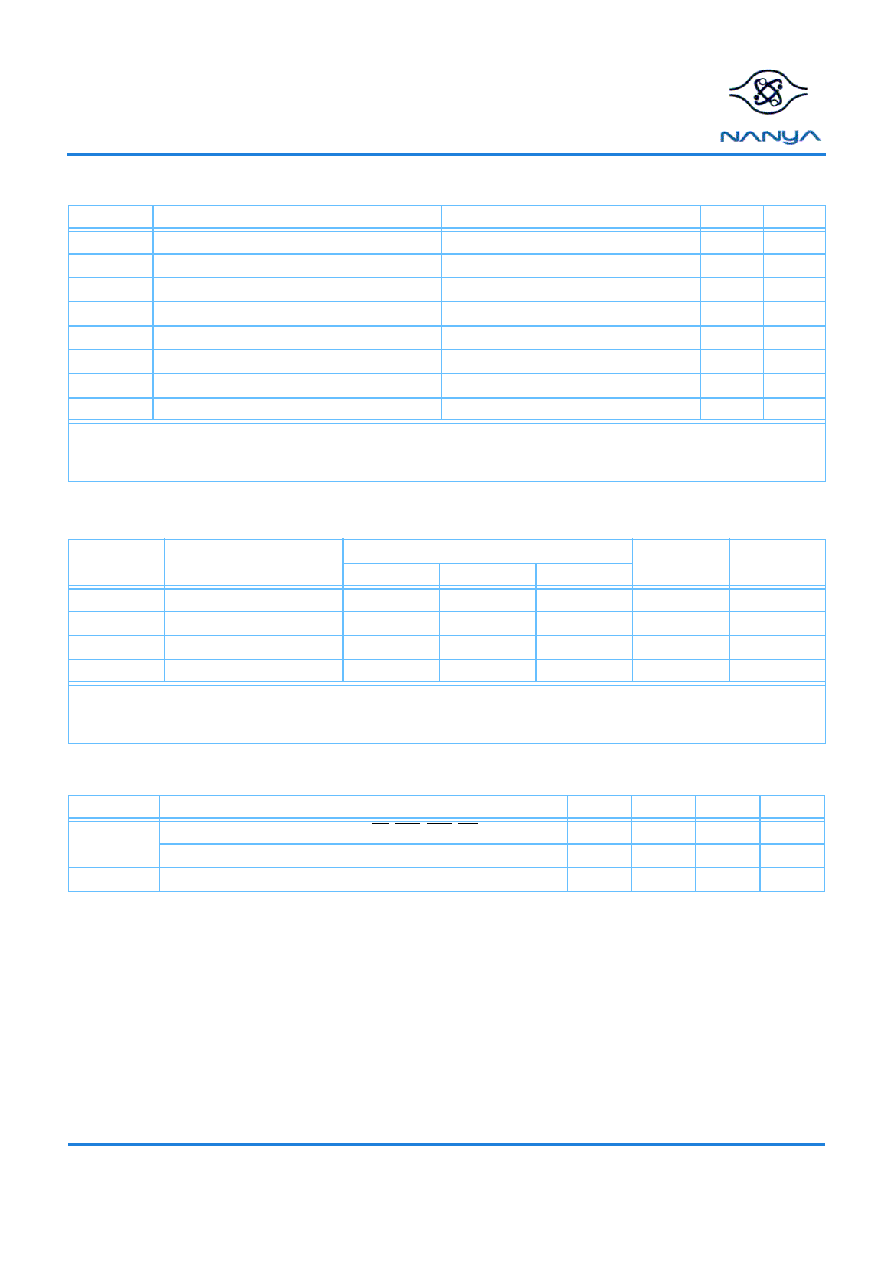
DC Output Load Circuit
Output
1200
50pF
3.3 V
870
V
OH
(DC) = 2.4V, I
OH
= -2mA
V
OL
(DC) = 0.4V, I
OL
= 2mA
NT5SV16M4DT
NT5SV8M8DT
NT5SV4M16DT
64Mb Synchronous DRAM
REV 1.1
10/01
15
©
NANYA TECHNOLOGY CORP
. All rights reserved.
NANYA TECHNOLOGY CORP. reserves the right to change Products and Specifications without notice.
Operating, Standby, and Refresh Currents
(T
A
= 0 to +70
∞
C, V
DD
= 3.3V
±
0.3V)
Parameter
Symbol
Test Condition
-6K
-7K
-7
Units
Notes
(6ns)
(7ns)
(7ns)
Operating Current
I
CC1
1 bank operation
t
RC
= t
RC
(min), t
CK
= min
Active-Precharge command cycling
without burst operation
60
55
mA
1, 2, 3
Precharge Standby Current
in Power Down Mode
I
CC2P
CKE
V
IL
(max), t
CK
= min,
CS = V
IH
(min)
1
mA
1
I
CC2PS
CKE
V
IL
(max), t
CK
= Infinity,
CS = V
IH
(min)
1
mA
1
Precharge Standby Current
in Non-Power Down Mode
I
CC2N
CKE
V
IH
(min), t
CK
= min,
CS = V
IH
(min)
10
mA
1, 5
I
CC2NS
CKE
V
IH
(min), t
CK
= Infinity,
5
mA
1, 7
No Operating Current
(Active state: 4 bank)
I
CC3N
CKE
V
IH
(min), t
CK
= min,
CS = V
IH
(min)
30
mA
1, 5
I
CC3P
CKE
V
IL
(max), t
CK
= min,
9
mA
1, 6
Operating Current (Burst
Mode)
I
CC4
t
CK
= min,
Read/ Write command cycling,
Multiple banks active, gapless data,
BL = 4
75
70
mA
1, 3, 4
Auto (CBR) Refresh Current
I
CC5
t
CK
= min, t
RC
= t
RC
(min)
CBR command cycling
120
110
mA
1
Self Refresh Current
I
CC6
CKE
0.2V
1
mA
1
1. Currents given are valid for a single device. The total current for a stacked device depends on the operation being performed
on the other deck.
2. These parameters depend on the cycle rate and are measured with the cycle determined by the minimum value of t
CK
and t
RC
.
Input signals are changed up to three times during t
RC
(min).
3. The specified values are obtained with the output open.
4. Input signals are changed once during t
CK
(min).
5. Input signals are changed once during three clock cycles.
6. Active Standby Current will be higher if Clock Suspend is entered during a burst read cycle (add 1mA per DQ).
7. Input signals are stable.
NT5SV16M4DT
NT5SV8M8DT
NT5SV4M16DT
64Mb Synchronous DRAM
REV 1.1
10/01
16
©
NANYA TECHNOLOGY CORP
. All rights reserved.
NANYA TECHNOLOGY CORP. reserves the right to change Products and Specifications without notice.
AC Characteristics
(T
A
= 0 to +70
∞
C, V
DD
= 3.3V
±
0.3V)
1. An initial pause of 200
µ
s, with DQM and CKE held high, is required after power-up. A Precharge All Banks command must
be given followed by a minimum of two Auto (CBR) Refresh cycles before or after the Mode Register Set operation.
2. The Transition time is measured between V
IH
and V
IL
(or between V
IL
and V
IH
)
3. In addition to meeting the transition rate specification, the clock and CKE must transit between V
IH
and V
IL
(or between V
IL
and V
IH
) in a monotonic manner.
4. Load Circuit A: AC timing tests have V
IL
= 0.4 V and V
IH
= 2.4 V with the timing referenced to the 1.40V crossover point
5. Load Circuit A: AC measurements assume t
T
= 1.0ns.
6. Load Circuit B: AC timing tests have V
IL
= 0.8 V and V
IH
= 2.0 V with the timing referenced to the 1.40V crossover point
7. Load Circuit B: AC measurements assume t
T
= 1.2ns.
.
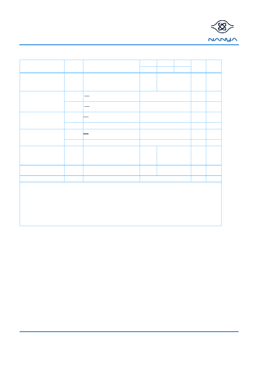
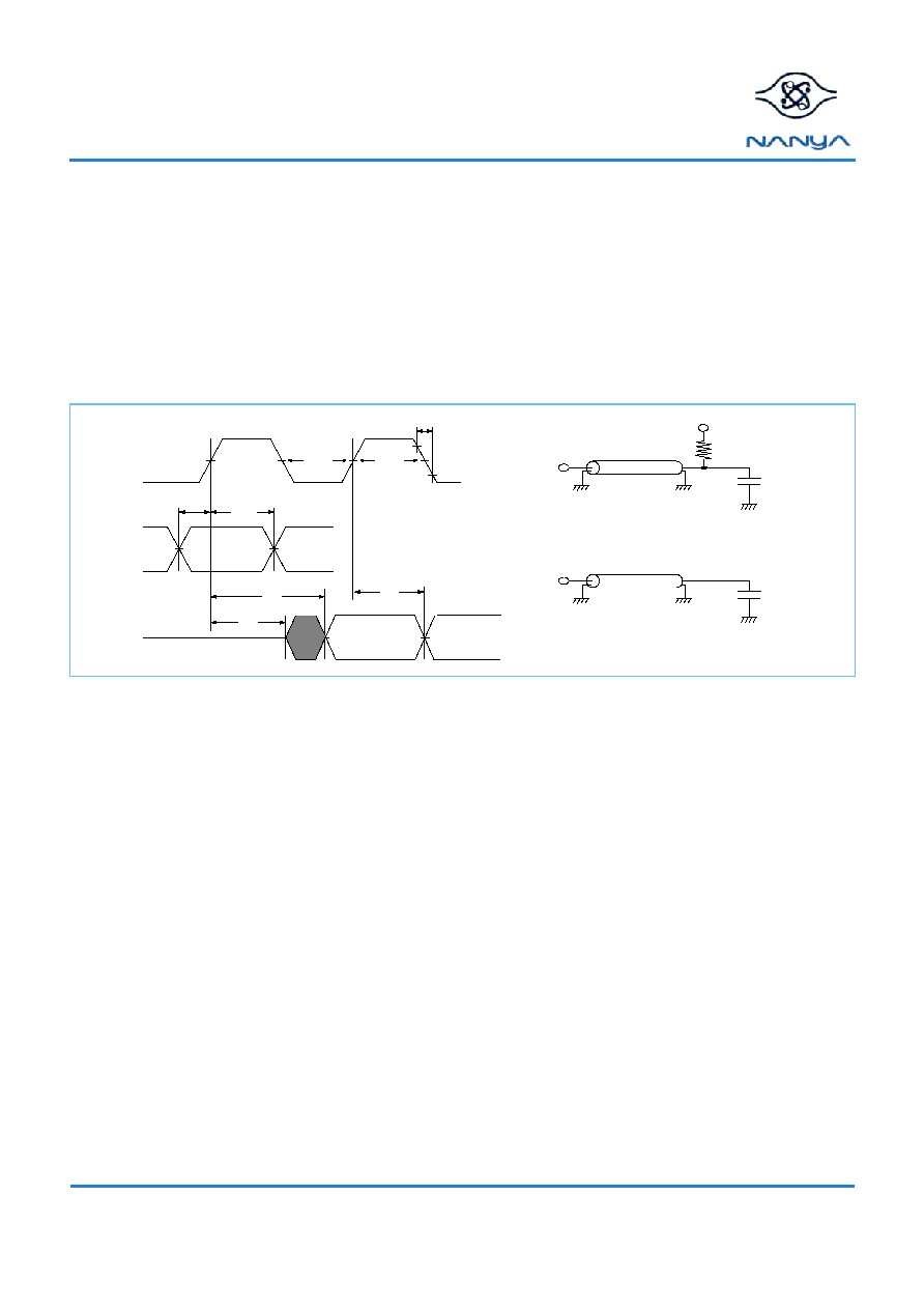
AC Characteristics Diagrams
Output
Input
Clock
t
OH
t
SETUP
t
HOLD
t
AC
t
LZ
1.4V
1.4V
1.4V
t
T
Vtt = 1.4V
Output
50
50pF
Z
o
= 50
AC Output Load Circuit (A)
t
CKH
t
CKL
Output
50pF
Z
o
= 50
AC Output Load Circuit (B)
V
IL
V
IH
NT5SV16M4DT
NT5SV8M8DT
NT5SV4M16DT
64Mb Synchronous DRAM
REV 1.1
10/01
17
©
NANYA TECHNOLOGY CORP
. All rights reserved.
NANYA TECHNOLOGY CORP. reserves the right to change Products and Specifications without notice.
Clock and Clock Enable Parameters
Symbol
Parameter
-6K
-7K
-7
Units
Notes
Min.
Max.
Min.
Max.
Min.
Max.
t
CK3
Clock Cycle Time, CAS Latency = 3
6
1000
7
1000
7
1000
ns
t
CK2
Clock Cycle Time, CAS Latency = 2
7.5
1000
7.5
1000
10
1000
ns
t
AC3 (A)
Clock Access Time, CAS Latency = 3
--
--
--
--
--
--
ns
1
t
AC2 (A)
Clock Access Time, CAS Latency = 2
--
--
--
--
--
--
ns
1
t
AC3 (B)
Clock Access Time, CAS Latency = 3
--
5.4
--
5.4
--
5.4
ns
2
t
AC2 (B)
Clock Access Time, CAS Latency = 2
--
5.4
--
5.4
--
6
ns
2
t
CKH
Clock High Pulse Width
2.5
--
2.5
--
3
--
ns
t
CKL
Clock Low Pulse Width
2.5
--
2.5
--
3
--
ns
t
CES
Clock Enable Set-up Time
1.5
--
1.5
--
2
--
ns
t
CEH
Clock Enable Hold Time
0.8
--
0.8
--
1
--
ns
t
SB
Power down mode Entry Time
0
6
0
7
0
7.5
ns
t
T
Transition Time (Rise and Fall)
0.5
10
0.5
10
0.5
10
ns
1. Access time is measured at 1.4V. See AC Characteristics: notes 1, 2, 3, 4, 5 and load circuit A.
2. Access time is measured at 1.4V. See AC Characteristics: notes 1, 2, 3, 6, 7 and load circuit B.
Common Parameters
Symbol
Parameter
-6K
-7K
-7
Units
Notes
Min.
Max.
Min.
Max.
Min.
Max.
t
CS
Command Setup Time
1.5
--
1.5
--
1.5
--
ns
t
CH
Command Hold Time
0.8
--
0.8
--
0.8
--
ns
t
AS
Address and Bank Select Set-up Time
1.5
--
1.5
--
1.5
--
ns
t
AH
Address and Bank Select Hold Time
0.8
--
0.8
--
0.8
--
ns
t
RCD
RAS to CAS Delay
15
--
15
--
20
--
ns
1
t
RC
Bank Cycle Time
48
--
52
--
63
--
ns
1
t
RAS
Active Command Period
36
100K
37
100K
42
100K
ns
1
t
RP
Precharge Time
15
--
15
--
20
--
ns
1
t
RRD
Bank to Bank Delay Time
12
--
14
--
14
--
ns
1
1. These parameters account for the number of clock cycle and depend on the operating frequency of the clock, as follows:
the number of clock cycles = specified value of timing / clock period (count fractions as a whole number).
Mode Register Set Cycle
Symbol
Parameter
-6K
-7K
-7
Units
Min.
Max.
Min.
Max.
Min.
Max.
t
RSC
Mode Register Set Cycle Time
12
--
14
--
14
--
ns
NT5SV16M4DT
NT5SV8M8DT
NT5SV4M16DT
64Mb Synchronous DRAM
REV 1.1
10/01
18
©
NANYA TECHNOLOGY CORP
. All rights reserved.
NANYA TECHNOLOGY CORP. reserves the right to change Products and Specifications without notice.
Read Cycle
Symbol
Parameter
-6K
-7K
-7
Units
Notes
Min.
Max.
Min.
Max.
Min.
Max.
t
OH
Data Out Hold Time
--
--
--
--
--
ns
1
3
--
3
--
3
--
ns
2, 4
t
LZ
Data Out to Low Impedance Time
--
0
--
0
--
ns
t
HZ3
Data Out to High Impedance Time
2.7
5.4
2.7
5.4
2.7
5.4
ns
3
t
HZ2
Data Out to High Impedance Time
2.7
5.4
2.7
5.4
3
6
ns
3
t
DQZ
DQM Data Out Disable Latency
2
--
2
--
2
--
CK
1. AC Output Load Circuit A.
2. AC Output Load Circuit B.
3. Referenced to the time at which the output achieves the open circuit condition, not to output voltage levels.
4. Data Out Hold Time with no load must meet 1.8ns (-5K, -7K, -75B).
Refresh Cycle
Symbol
Parameter
-6K
-7K
-7
Units
Notes
Min.
Max.
Min.
Max.
Min.
Max.
t
REF
Refresh Period
--
64
--
64
--
64
ms
1
t
SREX
Self Refresh Exit Time
10
--
10
--
10
--
ns
1. 4096 auto refresh cycles.
Write Cycle
Symbol
Parameter
-6K
-7K
-7
Units
Min.
Max.
Min.
Max.
Min.
Max.
t
DS
Data In Set-up Time
1.5
--
1.5
--
1.5
--
ns
t
DH
Data In Hold Time
0.8
--
0.8
--
0.8
--
ns
t
DPL
Data input to Precharge
12
--
14
--
14
--
ns
t
WR
Write Recovery Time
12
--
14
--
14
--
ns
t
DAL3
Data In to Active Delay
CAS Latency = 3
5
--
5
--
5
--
CK
t
DAL2
Data In to Active Delay
CAS Latency = 2
4
--
4
--
4
--
CK
t
DQW
DQM Write Mask Latency
0
--
0
--
--
CK
NT5SV16M4DT
NT5SV8M8DT
NT5SV4M16DT
64Mb Synchronous DRAM
REV 1.1
10/01
19
©
NANYA TECHNOLOGY CORP
. All rights reserved.
NANYA TECHNOLOGY CORP. reserves the right to change Products and Specifications without notice.
Clock Frequency and Latency
Symbol
Parameter
-6K
-7K
-7
Units
f
CK
Clock Frequency
166
133
143
133
143
100
MHz
t
CK
Clock Cycle Time
6
7.5
7
7.5
7
10
ns
t
AA
CAS Latency
3
2
3
2
3
2
CK
t
RP
Precharge Time
3
2
3
2
3
2
CK
t
RCD
RAS to CAS Delay
3
2
3
2
3
2
CK
t
RC
Bank Cycle Time
9
7
9
7
9
7
CK
t
RAS
Minimum Bank Active Time
6
5
6
5
6
5
CK
t
DPL
Data In to Precharge
2
2
2
2
2
2
CK
t
DAL
Data In to Active/Refresh
5
4
5
4
5
4
CK
t
RRD
Bank to Bank Delay Time
2
2
2
2
2
2
CK
t
WL
Write Latency
0
0
0
0
0
0
CK
t
DQW
DQM Write Mask Latency
0
0
0
0
0
0
CK
t
DQZ
DQM Data Disable Latency
2
2
2
2
2
2
CK
t
CSL
Clock Suspend Latency
1
1
1
1
1
1
CK
NT5SV16M4DT
NT5SV8M8DT
NT5SV4M16DT
64Mb Synchronous DRAM
REV 1.1
10/01
20
©
NANYA TECHNOLOGY CORP
. All rights reserved.
NANYA TECHNOLOGY CORP. reserves the right to change Products and Specifications without notice.
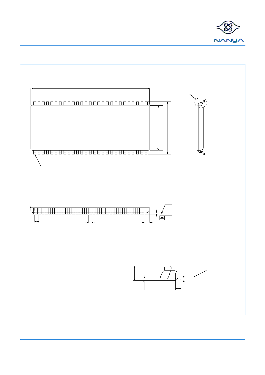
Package Dimensions
(400mil; 54 lead; Thin Small Outline Package)
Lead #1
0.80 Basic
0.35
1
0
.
1
6
±
0
.
1
3
22.22
±
0.13
1
1
.
7
6
±
0
.
2
0
-
0.05
+ 0.10
0.71REF
Detail A
0.10
Seating Plane
Detail A
0.5
±
0.1
0.05 Min
1
.
2
0
M
a
x
0.25 Basic
Gage Plane

NT5SV16M4DT
NT5SV8M8DT
NT5SV4M16DT
64Mb Synchronous DRAM
REV 1.1
10/01
21
©
NANYA TECHNOLOGY CORP
. All rights reserved.
NANYA TECHNOLOGY CORP. reserves the right to change Products and Specifications without notice.
Revision Log
Rev
Contents of Modification
05/01
Preliminary
09/01
Changed to Revision 1.0
Removed -75B speed grade
Added -7 speed grade.
Removed Icc6 low power product grade.
10/01
Changed to Revision 1.1
Changed tOH from 2.7ns to 3ns for all speed sort.