 | ÐлекÑÑоннÑй компоненÑ: NT68P61A | СкаÑаÑÑ:  PDF PDF  ZIP ZIP |
Äîêóìåíòàöèÿ è îïèñàíèÿ www.docs.chipfind.ru

NT68P61A
8-Bit Microcontroller for Monitor (24K OTP ROM Type)
1
V1.0
Features
T
40 pin DIP & 42 pin SDIP package
T
Operating Voltage Range: 4.5V to 5.5V
T
CMOS technology for low power consumption
T
Crystal oscillator or ceramic resonator* available
T
6502 8-bit CMOS CPU core
T
8MHz operation of frequency
T
24K bytes of OTP (one time programming) ROM
T
256 bytes of RAM (which stores EDID for DDC1/2B)
T
One 8-bit pre-loadable base timer
T
14 channels of 8 bit PWM outputs:
6 channel with 5V open drain and 8 channel with 12V
open drain
T
2 channel A/D converters with 6-bit resolution
T
24 bi-directional I/O port pins and 1 I/P pin
T
Hsync/Vsync signal processor
T
Hardware sync signals polarity & freq. evaluator
T
Built-In I
2
C bus interface
T
Supporting VESA DDC1/2B function
T
Six-interrupt sources
- INTV
(Vsync INT)
- INTE
(External INT with rising edge trigger)
- INTMR (Timer INT )
- INTA (Slave Address Matched INT)
- INTD (Shift Register INT)
- INTS
(SCL GO-LOW INT)
T
Hardware watch-dog timer function
T
Built-In Low Voltage reset circuit (LVRC)
General Description
NT68P61A is a monitor component
µ
C for auto-sync and
digital controlled applications. It contains a 6502
8-bit CPU core, 256 bytes of RAM used as working RAM
and stack area, 24K bytes of OTP ROM**, 14-channel 8-
bit PWM D/A converters, 2-channel A/D converters for
key detection saving I/O pins, one 8 bit pre-loadable
base timer, internal Hsync and Vsync signals processor
providing mode detection, watch-dog timer preventing
system from abnormal operation, and an I
2
C bus
interface. The LVRC enables NT68P61A operate
properly.
Users can store EDID data in the 128 bytes of RAM for
DDC1/2B, so that users can save the cost of dedicated
EEPROM for EDID. Half frequency output function can
save external one-shot circuit. All of these designs create
savings in component costs.
* The frequency deviation of ceramic resonator has
+/- 6% maximum.
** The NT6861 (MASK ROM type) will provide
4/8/12/16/24K bytes program ROM.

NT68P61A
2
Pin Configuration
[ O E ] D A C 2
D A C 1
D A C 0
[ D B 7 ] P 2 7
[ V P P ] R E S E T
V
D D
G N D
O S C O
O S C I
[ C E ] P 1 4
[ A 1 0 ] P 1 2 / H A L F H O
[ A 9 ] P 1 1 / A D 1
[ A 8 ] P 1 0 / A D 0
P 2 0 [ D B 0 ]
P 0 7 / H S Y N C O [ A 7 ]
P 3 1 / S C L [ A 1 3 ]
D A C 4 [ M O D E 0 ]
D A C 3 [ P G M ]
H S Y N C I
V S Y N C I / I N T V / [ A 1 4 ]
NT68P61A
1
2
3
4
5
6
7
8
9
1 0
1 1
1 2
1 3
1 4
1 5
1 6
2 5
2 6
2 7
2 8
2 9
3 0
3 1
3 2
3 3
3 4
3 5
3 6
3 7
3 8
3 9
4 0
P 1 5
[ A 1 1 ] P 1 3 / H A L F H I
P 1 6 / I N T E
1 7
1 8
1 9
2 0
2 4
2 3
2 2
2 1
D A C 5 [ M O D E 1 ]
D A C 6 [ M O D E 2 ]
D A C 7
P 2 1 [ D B 1 ]
P 2 2 [ D B 2 ]
P 0 6 / V S Y N C O [ A 6 ]
P 0 5 / D A C 1 3 [ A 5 ]
P 0 4 / D A C 1 2 [ A 4 ]
P 0 3 / D A C 1 1 [ A 3 ]
P 0 2 / D A C 1 0 [ A 2 ]
P 0 1 / D A C 9 [ A 1 ]
P 0 0 / D A C 8 [ A 0 ]
P 3 0 / S D A [ A 1 2 ]
[ D B 6 ] P 2 6
[ D B 5 ] P 2 5
[ D B 4 ] P 2 4
[ D B 3 ] P 2 3
* [ ]: OTP Mode
[ O E ] D A C 2
D A C 1
D A C 0
[ V P P ] R E S E T
V
D D
N C
G N D
O S C O
O S C I
P 1 5
[ A 1 1 ] P 1 3 / H A L F H I
[ A 9 ] P 1 1 / A D 1
[ A 8 ] P 1 0 / A D 0
P 0 0 / D A C 8 [ A 0 ]
P 1 6 / I N T E
P 0 1 / D A C 9 [ A 1 ]
P 0 2 / D A C 1 0 [ A 2 ]
P 0 3 / D A C 1 1 [ A 3 ]
P 0 4 / D A C 1 2 [ A 4 ]
P 0 6 / V S Y N C O [ A 6 ]
P 0 7 / H S Y N C O [ A 7 ]
D A C 6 [ M O D E 2 ]
N C
D A C 5 [ M O D E 1 ]
D A C 4 [ M O D E 0 ]
D A C 3 [ P G M ]
H S Y N C I
V S Y N C I / I N T V
D A C 7 [ A 1 4 ]
NT68P61AU
1
2
3
4
5
6
7
8
9
1 0
1 1
1 2
1 3
1 4
1 5
1 6
2 7
2 8
2 9
3 0
3 1
3 2
3 3
3 4
3 5
3 6
3 7
3 8
3 9
4 0
4 1
4 2
[ C E ] P 1 4
[ A 1 0 ] P 1 2 / H A L F H O
[ D B 7 ] P 2 7
[ D B 6 ] P 2 6
[ D B 5 ] P 2 5
[ D B 4 ] P 2 4
[ D B 3 ] P 2 3
1 7
1 8
1 9
2 0
2 1
P 0 5 / D A C 1 3 [ A 5 ]
P 3 1 / S C L [ A 1 3 ]
P 3 0 / S D A [ A 1 2 ]
P 2 0 [ D B 0 ]
P 2 1 [ D B 1 ]
P 2 2 [ D B 2 ]
2 6
2 5
2 4
2 3
2 2
* [ ]: OTP Mode
Block Diagram
T i m i n g G e n e r a t o r
C P U c o r e
6 5 0 2
Interrupt
Controller
H / V S y n c S i g n a l s
P r o c e s s o r
S R A M + S T A C K
2 5 6 B y t e s
W a t c h D o g T i m e r
P W M D A C s
I/O Ports
O S C I
O S C O
V
D D
G N D
H S Y N C I
I N T E
S C L
S D A
D A C 0 - D A C 7
P 0 0 - P 0 7
P 1 0 - P 1 5
P 2 0 - P 2 7
V S Y N C O
A/D Converter
A D 0 - A D 1
8 Bit Base Timer
P 3 0 - P 3 1
IIC BUS
P 1 6
H S Y N C O
H A L F H I
H A L F H O
D A C 8 - D A C 1 3
V S Y N C I / I N T V
O T P P r o g r a m R O M
2 4 K B y t e s
L V R C

NT68P61A
3
Pin Descriptions
Pin No.
Designation
Reset Init.
I/O
Description
40 Pin
42 Pin
1
1
DAC2
[ OE ]
O
[ I ]
Open drain 12V, D/A converter output 2
[OTP ROM program output enable]
2
2
DAC1
O
Open drain 12V, D/A converter output 1
3
3
DAC0
O
Open drain 12V, D/A converter output 0
4
4
RESET
[ VPP ]
I
[ P ]
Schmitt trigger input pin, low active reset**
[OPT ROM program supply voltage]
5
5
V
DD
P
Power
6
7
GND
P
Ground
7
8
OSCO
O
Crystal OSC output
8
9
OSCI
I
Crystal OSC input
9
10
P15
I/O
Bi-directional I/O pin
10
11
P14
[ CE ]
I/O
[ I ]
Bi- directional I/O pin
[OTP ROM program chip enable]
11
12
P13/HALFHI
[ A11 ]
P13
I/O
[ I ]
Bi- directional I/O pin, shared with half hsync input
[OTP ROM program address buffer]
12
13
P12/HALFHO
[ A10 ]
P12
I/O
[ I ]
Bi- directional I/O pin, shared with half hsync output
[OTP ROM program address buffer]
13
14
P11/AD1
[ A9 ]
P11
I/O
[ I ]
Bi- directional I/O pin, shared with A/D converter channel
1 input
[OTP ROM program address buffer]
14
15
P10/AD0
[ A8 ]
P10
I/O
[ I ]
Bi- directional I/O pin, shared with A/D converter
channel 0 input
[OTP ROM program address buffer]
15
16
P16/INTE
P16
I
Schmitt trigger input pin
with internal pull high,
shared
with external Rising-edge trigger interrupt
16 - 23
17 - 24
P27 - P20
[ DB7 ] -
[ DB0 ]
I/O
[ I/O ]
Bi- directional I/O pin, push-pull structure with high current
drive/sink capability
[OTP ROM program data buffer]
24
25
P30/SDA
[ A12 ]
P30
I/O
[ I ]
Open drain 5V Bi-direction I/O pin P30, shared with SDA
pin of I
2
C bus schmitt trigger buffer
[OTP ROM program address buffer]
25
26
P31/SCL
[ A13 ]
P31
I/O
[ I ]
Open drain 5V Bi-direction I/O pin P31, shared with SCL
pin of I
2
C bus schmitt trigger buffer
[OTP ROM program address buffer]
26
27
P00/DAC8
[ A0 ]
P00
I/O
[ I ]
Bi- directional I/O pin, shared with open drain 5V D/A
converter output 8
[OTP ROM program address buffer]
* [ ]: OTP Mode
** This RESET pin must be pulled high by external pulled-up resistor (5K
suggestion), or it will stay low
voltage to reset system all the time.

NT68P61A
4
Pin Descriptions (continued)
Pin No.
Designation
Reset Init.
I/O
Description
40 Pin
42 Pin
27
28
P01/DAC9
[ A1 ]
P01
I/O
[ I ]
Bi- directional I/O pin, shared with open drain 5V D/A
converter output 9
[OTP ROM program address buffer]
28
29
P02/DAC10
[ A2 ]
P02
I/O
[ I ]
Bi- directional I/O pin, shared with open drain 5V D/A
converter output 10
[OTP ROM program address buffer]
29
30
P03/DAC11
[ A3 ]
P03
I/O
[ I ]
Bi- directional I/O pin, shared with open drain 5V D/A
converter output 11
[OTP ROM program address buffer]
30
31
P04/DAC12
[ A4 ]
P04
I/O
[ I ]
Bi- directional I/O pin, shared with open drain 5V D/A
converter output 12
[OTP ROM program address buffer]
31
32
P05/DAC13
[ A5 ]
P05
I/O
[ I ]
Bi- directional I/O pin, shared with open drain 5V D/A
converter output 13
[OTP ROM program address buffer]
32
33
P06/VSYNCO
[ A6 ]
P06
I/O
[ I ]
Bi- directional I/O pin, shared with vsync out
[OTP ROM program address buffer]
33
34
P07/HSYNCO
[ A7 ]
P07
I/O
[ I ]
Bi-directional I/O pin, shared with hsync out
[OTP ROM program address buffer]
34
35
DAC7
[ A14 ]
O
Open drain 12V, D/A converter output
[OTP ROM program address buffer]
35
36
DAC6
[ MODE2 ]
O
[ I ]
Open drain 12V, D/A converter output
[OTP ROM mode select]
36
38
DAC5
[ MODE1 ]
O
[ I ]
Open drain 12V, D/A converter output
[OTP ROM mode select]
37
39
DAC4
[ MODE0 ]
O
[ I ]
Open drain 12V, D/A converter output
[OTP ROM mode select]
38
40
DAC3
[ PGM ]
O
[ I ]
Open drain 12V, D/A converter output
[OTP ROM program control]
39
41
HSYNCI
I
Debouncing & schmitt trigger input pin for video horizontal
sync signal, internal pull high, shared with composite sync
input
40
42
VSYNCI/INTV
[A14]
VSYNCI
I
[ I ]
Debouncing & schmitt trigger input pin for video vertical
sync signal, internal pull high, shared with external
interrupt source
-
6
NC
I/O
Bi-directional I/O pin, with internal pulled up 22K
resister, only 42 pin SDIP available
-
37
NC
I/O
Bi-directional I/O pin, with internal pulled up 22K
resister, only 42 pin SDIP available
* [ ]: OTP Mode

NT68P61A
5
Functional Descriptions
1. 6502 CPU
The 6502 is an 8-bit CPU that provides 56 instructions, decimal and binary arithmetic, thirteen addressing modes, true
indexing capability, programmable stack pointer with variable length stack, a wide selection of addressable memory, and
interrupt input options.
The CPU clock cycle is 4MHz (8MHz system clock divided by 2). Refer to 6502 data sheet for more details.
Accumulator A
Index Register Y
0
7
7
Index Register X
7
0
0
Stack Pointer SP
0
N
Status Register P
0
7
Carry
Zero
IRQ Disable
Decimal Mode
B R K C o m m a n d
Overflow
Negative
7
Program Counter PCH
8
1 5
7
0
P C L
1 = T R U E
1 = Result ZERO
1 = D I S A B L E
1 = T R U E
1 = N E G
1 = T R U E
1 = B R K
V
B
D
I
Z
C
Figure 1. 6502 CPU Registers and Status Flags

NT68P61A
6
2. Instruction Set List
Instruction Code
Meaning
Operation
ADC
Add with carry
A + M + C
A, C
AND
Logical AND
A
·
M
A
ASL
Shift left one bit
C
M7
·
·
·
M0
0
BCC
Branch if carry clears
Branch on C = 0
BCS
Branch if carry sets
Branch on C = 1
BEQ
Branch if equal to zero
Branch on Z = 1
BIT
Bit test
A
·
M, M7
N, M6
V
BMI
Branch if minus
Branch on N = 1
BNE
Branch if not equal to zero
Branch on Z = 0
BPL
Branch if plus
Branch on N = 0
BRK
Break
Forced Interrupt PC+2
PC
BVC
Branch if overflow clears
Branch on V = 0
BVS
Branch if overflow sets
Branch on V = 1
CLC
Clear carry
0
C
CLD
Clear decimal mode
0
D
CLI
Clear interrupt disable bit
0
J
CLV
Clear overflow
0
V
CMP
Compare accumulator to memory
A
-
M
CPX
Compare with index register X
X
-
M
CPY
Compare with index register Y
Y
-
M
DEC
Decrement memory by one
M
-
1
M
DEX
Decrement index X by one
X
-
1
X
DEY
Decrement index Y by one
Y
-
1
Y
EOR
Logical exclusive-OR
A
M
A
INC
Increment memory by one
M + 1
M
INX
Increment index X by one
X + 1
X
INY
Increment index Y by one
Y + 1
Y
NT68P61A
7
Instruction Set List (continued)
Instruction Code
Meaning
Operation
JMP
Jump to new location
(PC+1)
PCL, (PC+2)
PCH
JSR
Jump to subroutine
PC + 2
, (P+1)
PCL,
(PC+2)
PCH
LDA
Load accumulator with memory
M
A
LDX
Load Index register X with memory
M
X
LDY
Load Index register Y with memory
M
Y
LSR
Shift right one bit
0
M7
·
·
·
M0
C
NOP
No operation
No operation (2 cycles)
ORA
Logical OR
A + M
A
PHA
Push accumulator on stack
A
PHP
Push status register on stack
P
PLA
Pull accumulator from stack
A
PLP
Pull status register from stack
P
ROL
Rotate left through carry
C
M7
·
·
·
M0
C
ROR
Rotate right through carry
C
M7
·
·
·
M0
C
RTI
Return from interrupt
P
, PC
RTS
Return from subroutine
PC
, PC+1
PC
SBC
Subtract with borrow
A
-
M
-
C
A, C
SEC
Set carry
1
C
SED
Set decimal mode
1
D
SEI
Set interrupt disable status
1
J
STA
Store accumulator in memory
A
M
STX
Store index register X in memory
X
M
STY
Store index register Y in memory
Y
M
TAX
Transfer accumulator to index X
A
X
TAY
Transfer accumulator to index Y
A
Y
TSX
Transfer stack pointer to index X
S
X
TXA
Transfer index X to accumulator
X
A
TXS
Transfer index X to stack Pointer
X
S
TYA
Transfer index Y to accumulator
Y
A
* Refer to 6502 programming data book for more details.
NT68P61A
8
3. OTP ROM: 24K X 8 bits
The OTP ROM storing application program code, executed by 6502 CPU, has a capacity of 24K X 8 bits, addressed from
$A000 to $FFFF. It is programmed by the universal EPROM writer through a conversion adapter.
In PROGRAMMING mode, OTP ROM is integrated with system and cannot be directly accessed. When using the OTP
ROM alone, first enter the PROGRAMMING mode by setting: RESET = VPP.
At this time, through multiplex pins, normal procedures are used to program and verify the OTP ROM block with the
universal programmer.
OTP ROM Mega Cell D.C. Electrical Characteristics (READ Mode)
(V
DD
= 5V , T
A
= 25
°
C, unless otherwise specified)
Symbol
Parameter
Min.
Typ.
Max.
Unit
Test Conditions
Note
V
IH
V
DD
-0.3
V
DD
+0.3
V
1
V
IL
Input Voltage
-0.3
0.3
V
1
I
IL
Input Current
+/-10
µ
A
I
OH
-400
µ
A
V
DD
=5V, V
OH
= 4.5V
I
OL
Output Voltage
1
µ
A
V
DD
=5V, V
OL
= 0.5V
I
DD
Operating Current
1
µ
A
f = 4MHz
2
ISTB1
Standby Current
100
µ
A
3
Notes: 1. All inputs and outputs are CMOS compatible
2. f = 4MHz, Iout = 0mA, CE = V
IH
, V
DD
= 5V
3. CE = V
IH
, OE = V
IL
, V
DD
= 5V
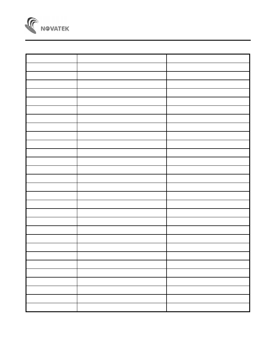
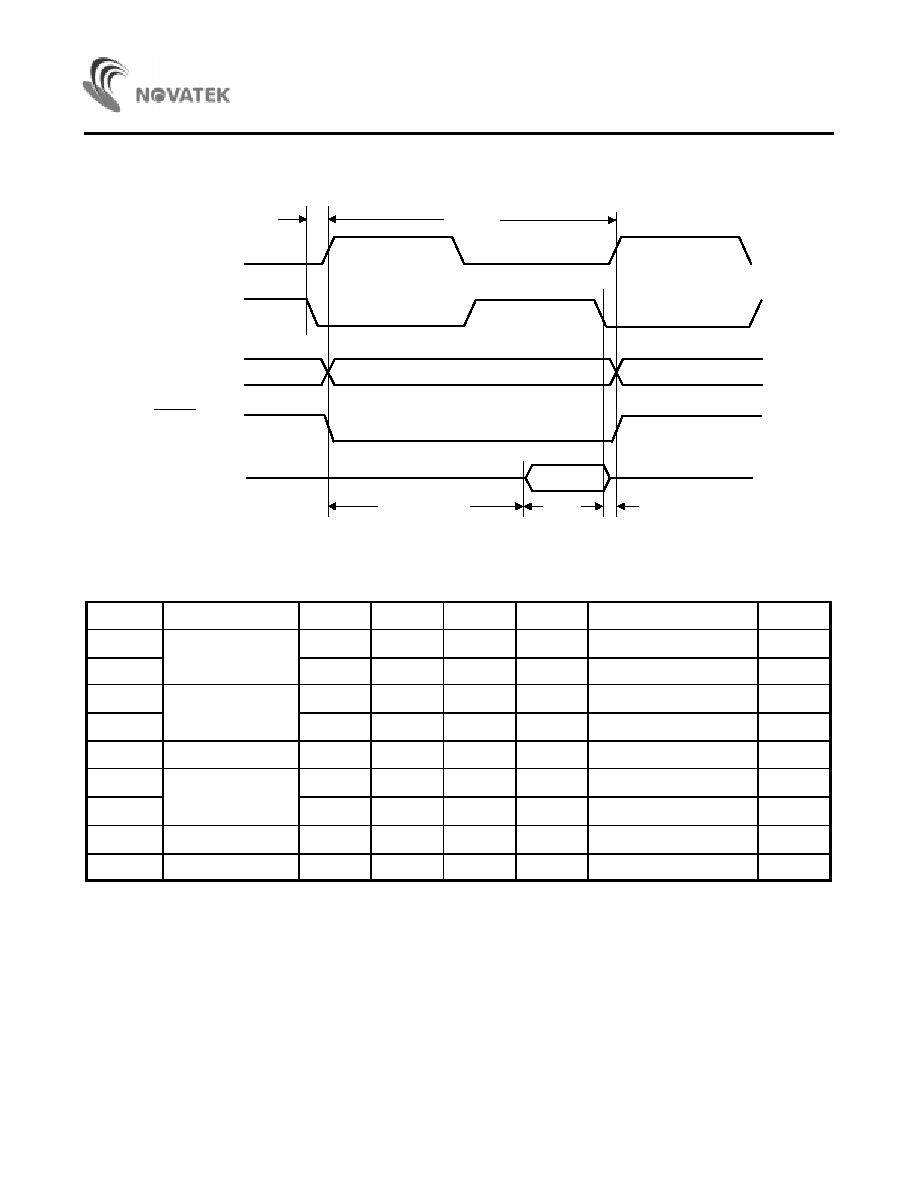
OTP ROM Mega Cell l A.C. Electrical Characteristics (READ Mode)
(V
DD
= 5V, T
A
= 25
°
C, unless otherwise specified)
Symbol
Parameter
Min.
Max.
Unit
Conditions
Tcyc
Cycle Time
250
ns
T12
Nonoverlap Time to PH1 & PH2
5
65
ns
Tacc
Address Access Time
145
ns
Tce
OTPCE to Output Valid
145
ns
4.5V < V
DD
< 5.5V
Tst
Output Data Setup Time
20
ns
Toh
Output Data Hold Time
0
ns
OTP ROM MEGA CELL A.C. Test Conditions
Output Load
1 CMOS Gate and CL = 10pF
Input Pulse Rise and Fall Times
10ns Max.
Input Pulse Levels
0V to 5V
Timing Measurement Reference Level
Inputs 0V and 5V outputs 0.3V and 4.7V
NT68P61A
9
OTP ROM Mega Cell Timing Waveforms (READ Mode)
Tcyc
T 1 2
Tacc & Tce
Tst
T o h
P H 1
P H 2
A0 - A14
O T P C E
DB0 - DB7
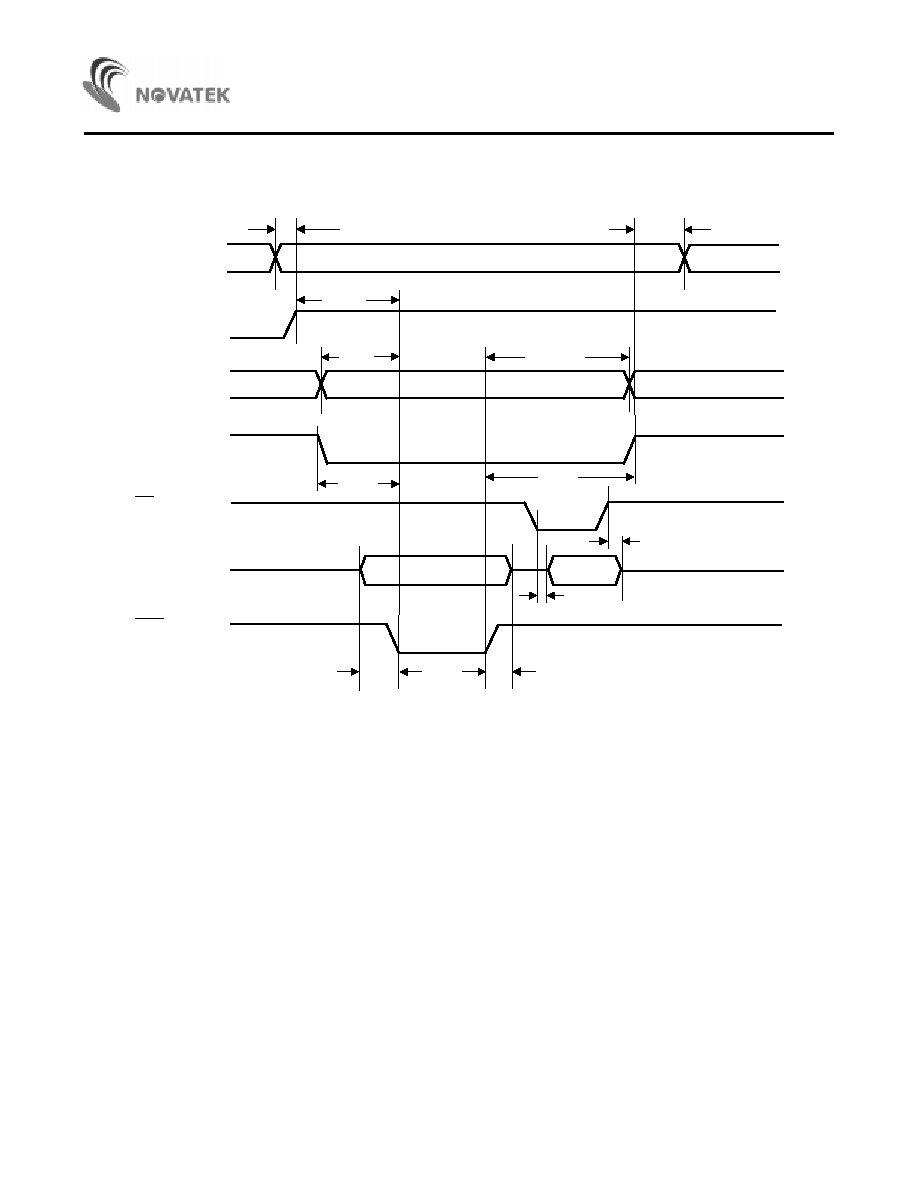
OTP ROM Mega Cell A.C. Electrical Characteristics (PROGRAMMING Mode)
(T
A
= 25
°
C, unless otherwise specified)
Symbol
Parameter
Min.
Typ.
Max.
Unit
Test Conditions
Note
V
DD
Supply Voltage
6
6.5
V
4
VPP
10.5
12.75
V
V
IH
Input Voltage
2
V
DD
+0.3
V
V
IL
-0.3
0.8
V
IIL
Input Current
+/-10
µ
A
I
OH
Output Current
-400
µ
A
V
DD
= 5V, V
OH
= 4.5V
I
OL
1
mA
V
DD
= 5V, V
OL
= 0.5V
I
DD
Programming
30
mA
IPP
Current
20
mA
VPP = 12.75V
Note: 4. For reliability concern, we suggested V
DD
= 6V & VPP = 12.75V for test OTP ROM AC characteristics in
PROGRAMMING mode, using the same condition for the universal programmer supply voltage.
NT68P61A
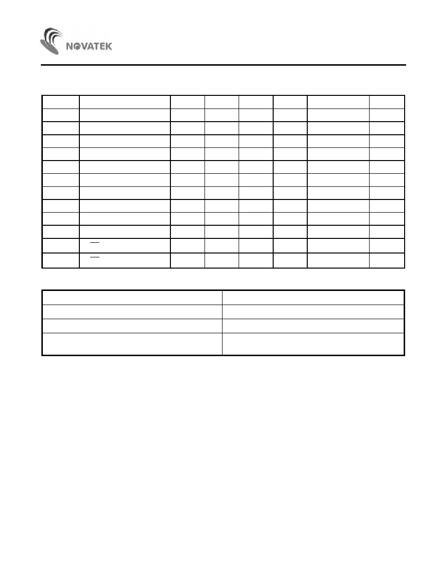
10
OTP ROM Mega Cell D.C. Electrical Characteristics (PROGRAMMING Mode)
(T
A
= 25
°
C, unless otherwise specified)
Symbol
Parameter
Min.
Typ.
Max.
Unit
Test Conditions
Note
Tms
Mode Decode Setup Time
2
ms
Tmh
Mode Decode Hold Time
2
ms
Tas
Address Setup Time
2
ms
Tah
Address Hold Time
2
ms
Tces
CE Setup Time
2
ms
Tceh
CE Hold Time
2
ms
Tds
Data Setup Time
2
ms
Tdh
Data Hold Time
2
ms
Tvs
VPP Setup Time
2
ms
Tpw
Program Pulse Width
100
ms
Tdv
OE to Output Valid
150
ns
Tdf
OE to Output in High-Z
90
ns
CE = V
IL
OTP ROM Mega Cell A.C. Test Conditions
Output Load
1 TTL Gate and CL = 100pF
Input Pulse Rise and Fall Times
10ns Max.
Input Pulse Levels
0.45V to 2.4V
Timing Measurement Reference Level
Inputs 0.8V and 2.2V
Outputs 0.8V and 2.4V
Note: 5. V
DD
must be applied simultaneously or before VPP and cut off simultaneously or after V
PP
.
6. Removing the device from power or setting the device with V
PP
= 12.75V may cause permanent damage
to the device.
NT68P61A
11
OTP ROM Mega Cell Timing Waveforms (PROGRAM Mode)
A0 - A14
DB0 - DB7
C E
O E
P G M
V P P
MODE DEC.
TEST = VPP, MODE [0..2] = 000;
D IN
D O U T
T m s
T m h
Tds
T p w
Tdh
Tdv
Tdf
Tvs
Tas
Tces
Tceh
Tah

NT68P61A
12
OTP ROM Mega cell Mode Selection
RESET
= 12.75V,
OSCI = V
IL
,
P16 = V
IH
, DAC0 = V
IL
Mode [0..2]
Mode
CE
OE
VPP
DB0 -
DB7
not VPP
- - -
Normal Operating
-
-
-
-
VPP
000
Output Disable
-
V
IH
-
high-Z
VPP
000
Program
V
IH
V
IH
VPP
data in
VPP
000
Program Verify
V
IH
V
IL
VPP
data out
VPP
000
Program Inhibit (Standby)
V
IL
-
VPP
high-Z
VPP
001
Security (Program)
V
IH
-
VPP
data in
VPP
010
Word-line Stress
-
-
VPP
-
VPP
011
Bit-line Stress
-
-
VPP
"0"
VPP
100
OTP Row (after pkg)
V
IH
V
IH
VPP
data in
VPP
101
OTP Column (after pkg)
V
IH
V
IH
VPP
data in
* The security byte is at address $0000.
READ
NT68P61A's OTP ROM mega cell has 2 control pins. CE
(Chip Enable) controls the operation power and is used
for device selection. The OE (Output Enable) controls
the output buffers.
OUTPUT DISABLE
If OE = V
IH
, the outputs will be in a high impedance
state. Two or more ROMs can be connected together on
a common bus.
STANDBY
By applying a low power level to the CE input, the chip
enters STANDBY reducing the operating current to
100
µ
A.
PROGRAM
Initially, all bits are in "1" state which is the erased state.
The program operation is to introduce "0" data into the
desired bit locations by electrical programming. When
the VPP input is at 12.75V and CE is at V
IH
, the chip
enters the PROGRAMMING mode.
PROGRAM VERIFY
The VERIFY mode is to check if the desired data is
correctly programmed on the programmed bit. The
VERIFY is accomplished with CE at V
IH
, VPP input is at
12.75V, and OE = V
IL
.
PROGRAM INHIBIT
Using this mode, programming of two or more OTP
ROMs in parallel with different data is accomplished. All
inputs except for CE and OE may be commonly
connected, and a TTL high level program pulse is
applied to the CE of the desired device only and TTL
high level signal is applied to the other devices.
NT68P61A
13
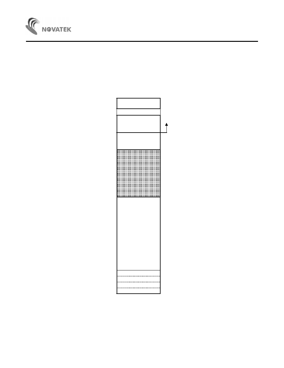
4. RAM: 256 X 8 bits
256 X 8-bit SRAM is used for data memory and stack. The RAM addressing range is from $0080 to $017F. From $0100 to
$017F is used as the EDID data buffer when activating DDC1/2B mode transmission. The contents of RAM are
undetermined at power-up and are not affected by system reset. Software programmers can allocate stack area in the
RAM by setting stack pointer register S. Because the 6502 default stack pointer is $01FF, programmers must set register
S to FFH when starting the program, so the stack area will map $01FF - $0180 to $00FF - $0080.
as;
LDX
#$FF
TXS
R A M
Unused
$ 0 0 0 0
$ 0 0 8 0
$ 0 1 0 0
$ 0 0 F F
$A000
$ F F F F
stack pointer
$ F F F E
$ F F F D
$ F F F C
R S T - L
R S T - H
I R Q - L
I R Q - H
R E S E T v e c t o r
IRQ vector
$ 0 1 7 F
E D I D
$ 0 1 8 0
(24K Bytes)
O T P
R O M
$ 0 0 2 5
System Registers
U n u s e d
$BFFF
NT68P61A
14
5. System Registers
Addr.
Register
INIT
Bit7
Bit6
Bit5
Bit4
Bit3
Bit2
Bit1
Bit0
$0000
PT0
FFH
P07
P06
P05
P04
P03
P02
P01
P00
RW
$0001
PT1
7FH
-
P16
P15
P14
P13
P12
P11
P10
RW
$0002
PT2DIR
FFH
P27OE
P26OE
P25OE
P24OE
P23OE
P22OE
P21OE
P20OE
W
$0003
PT2
FFH
P27
P26
P25
P24
P23
P22
P21
P20
RW
$0004
PT3
03H
-
-
-
-
-
-
P31
P30
RW
$0005
MD CON
07H
-
-
-
-
-
-
-
-
-
INSEN
-
HSEL
S/ C
S/ C
MD1/ 2
MD1/ 2
R
W
$0006
HV CON
2FH
HCNTOV
VCNTOV
HSYNCI
VSYNCI
HPOLI
VPOLI
HPOLO
VPOLO
R
W
$0007
HCNT L
00H
HCL7
HCL6
HCL5
HCL4
HCL3
HCL2
HCL1
HCL0
R
$0008
HCNT H
00H
-
-
-
-
HCH3
HCH2
HCH1
HCH0
R
$0009
VCNT L
00H
VCL7
VCL6
VCL5
VCL4
VCL3
VCL2
VCL1
VCL0
R
$000A
VCNT H
00H
-
-
-
-
VCH3
VCH2
VCH1
VCH0
R
$000B
SYNCON
FFH
NOHALF
ENHALF
-
FRUN
FRFREQ
HALFPOL
ENH
ENV
W
$000C
ENDAC
FFH
ENAD1
ENAD0
ENDK13
ENDK12
ENDK11
ENDK10
ENDK9
ENDK8
W
$000D
AD0 REG
C0H
CEND
CSTA
AD05
AD04
AD03
AD02
AD01
AD00
R
W
$000E
AD1 REG
00H
-
-
AD15
AD14
AD13
AD12
AD11
AD10
R
$000F
IEX
00H
-
-
IEINTS
IEINTD
IEINTA
IEINTR
IEINTE
IEINTV
W
NT68P61A
15
System Registers (continued)
Addr.
Register
INIT
Bit7
Bit6
Bit5
Bit4
Bit3
Bit2
Bit1
Bit0
$0010
IRQX
00H
-
-
IRQINTS
IRQINTD
IRQINTA
IRQINTR
IRQINTE
IRQINTV
R
$0011
CLR FLG
00H
CLRHOV
CLRVOV
CLRINTS
CLRINTD
CLRINTA
CLRINTR
CLRINTE
CLRINTV
W
$0012
CLR WDT
-
0
1
0
1
0
1
0
1
W
$0013
II ADR
FFH
AR7
AR6
AR5
AR4
AR3
AR2
AR1
-
W
$0014
II DAT
00H
SR7
SR6
SR5
SR4
SR3
SR2
SR1
SR0
RW
$0015
II STS
08H
-
-
START
START
STOP
STOP
ENDDC
TRX
RXAK
-
R
W
$0016
BT
00H
BT7
BT6
BT5
BT4
BT3
BT2
BT1
BT0
W
$0017
BT CON
03H
-
-
-
-
-
-
TBS
ENBT
W
$0018
DACH0
80H
DKVL7
DKVL6
DKVL5
DKVL4
DKVL3
DKVL2
DKVL1
DKVL0
RW
$0019
DACH1
80H
DKVL7
DKVL6
DKVL5
DKVL4
DKVL3
DKVL2
DKVL1
DKVL0
RW
$001A
DACH2
80H
DKVL7
DKVL6
DKVL5
DKVL4
DKVL3
DKVL2
DKVL1
DKVL0
RW
$001B
DACH3
80H
DKVL7
DKVL6
DKVL5
DKVL4
DKVL3
DKVL2
DKVL1
DKVL0
RW
$001C
DACH4
80H
DKVL7
DKVL6
DKVL5
DKVL4
DKVL3
DKVL2
DKVL1
DKVL0
RW
$001D
DACH5
80H
DKVL7
DKVL6
DKVL5
DKVL4
DKVL3
DKVL2
DKVL1
DKVL0
RW
$001E
DACH6
80H
DKVL7
DKVL6
DKVL5
DKVL4
DKVL3
DKVL2
DKVL1
DKVL0
RW
$001F
DACH7
80H
DKVL7
DKVL6
DKVL5
DKVL4
DKVL3
DKVL2
DKVL1
DKVL0
RW
$0020
DACH8
80H
DKVL7
DKVL6
DKVL5
DKVL4
DKVL3
DKVL2
DKVL1
DKVL0
RW
$0021
DACH9
80H
DKVL7
DKVL6
DKVL5
DKVL4
DKVL3
DKVL2
DKVL1
DKVL0
RW
$0022
DACH10
80H
DKVL7
DKVL6
DKVL5
DKVL4
DKVL3
DKVL2
DKVL1
DKVL0
RW
$0023
DACH11
80H
DKVL7
DKVL6
DKVL5
DKVL4
DKVL3
DKVL2
DKVL1
DKVL0
RW
$0024
DACH12
80H
DKVL7
DKVL6
DKVL5
DKVL4
DKVL3
DKVL2
DKVL1
DKVL0
RW
$0025
DACH13
80H
DKVL7
DKVL6
DKVL5
DKVL4
DKVL3
DKVL2
DKVL1
DKVL0
RW
Note: The line above a writable signal name indicate an active low signal
The dash line in these control register indicate an undefined bit
The address of control register from $0026 to $007F are not used.
NT68P61A
16
6. Timing Generator
This block generates the system timing and control signal to be supplied to the CPU and on-chip peripherals. A crystal
quartz, ceramic resonator, or an external clock signal provided to the OSCI pin generates 8MHz system clock,
(4 MHz for CPU), Although internal circuits have a feedback resistor and capacitor included, components may be
externally added to ensure proper operation. The typical clock frequency is 8MHz. This frequency will affect the operation
of on-chip peripherals whose operating frequency is based on the system clock .
8MHz
O S C I
O S C O
NT68P61A
O S C I
NT68P61A
(1)
(2)
Unconnected
External Clock
O S C O
Figure 2. Oscillator Connections
7. A/D Converter
The analog to digital converter is a single 6-bit successive approximation converter. Analog voltage is supplied from
external sources to the A/D input pins and the results of the conversion are stored in the 6-bit data latch registers
($000D & $000E). The A/D converter is controlled by the control bits in the A/D control register ENDAC. Refer to the A/D
channel format table A/D input pins activation. A conversion is started by setting a '0' to the CONVERSION START bit
( CSTA ) in the A/D control register ($000D). This automatically sets the CONVERSION END bit ( CEND ) to '1'. When a
conversion has been finished, CEND
bit automatically clears to '0'. The A/D conversion data in the AD LATCH registers
($000D & $000E) is valid digital data.
The analog voltage to be measured should be stable during the conversion operation. The variation should exceed
1/2 LSB for accuracy in measurement. Please refer Figure 3 for checking the linearity of A/D.
A/D Channel Format Table
ENAD1
ENAD0
P11 line
P10 line
0
0
AD1
AD0
0
1
AD1
P10
1
0
P11
AD0
1
1
P11
P10

NT68P61A
17
A/D Channel Control Register
Addr.
Register
INIT
Bit7
Bit6
Bit5
Bit4
Bit3
Bit2
Bit1
Bit0
$000C
ENDAC
FFH
ENAD1
ENAD0
ENDK13
ENDK12
ENDK11
ENDK10
ENDK9
ENDK8
W
$000D
AD0 REG
C0H
CEND
CSTA
AD05
AD04
AD03
AD02
AD01
AD00
R
W
$000E
AD1 REG
00H
-
-
AD15
AD14
AD13
AD12
AD11
AD10
R
Input Voltage
Digital Value
Input Voltage
Digital Value
Input Voltage
Digital Value
0.12
0 ($00)
1.79
23 ($17)
3.5
46 ($2E)
0.37
1 ($01)
2.03
27 ($1B)
3.75
49 ($31)
0.53
7 ($07)
2.27
30 ($1E)
3.99
52 ($34)
0.78
10 ($0A)
2.51
33 ($21)
4.22
56 ($38)
1
14 ($0E)
2.76
36 ($24)
4.46
63 ($3F)
1.28
17 ($11)
3
40 ($28)
4.7
63 ($3F)
1.54
20 ($14)
3.25
43 ($2B)
4.95
63 ($3F)
Input Voltage
Digital Value
0
0.2
0.4
0.6
0.8
1
0
10
20
30
40
50
60
70
Linear Range
0.3
0.7
These digitals have 1 LSB deviation
±
V
D D
Figure 3. A/D Converter Linearity Diagram
NT68P61A
18
8. PWM DACs (Pulse Width Modulation D/A Converters)
There are 14 PWM D/A converters with 8-bit resolution in NT68P61A. Eight of these D/A (DAC0 - DAC7) converters are
open-drain output structures with 12V applied (maximum), and the other six D/A converters (DAC8 - DAC13) are
open-drain output structures with 5V applied (maximum). The PWM frequency is 31.25 KHz on 8 MHz system clock. Use
of a different oscillator frequency will result in different PWM frequency. As DAC8 - DAC13 are shared with I/O port pins,
user can write '0' to corresponding enable bit in the ENDAC control register to activate each of DACH8 - 13. There are 14-
channel readable DACH registers corresponding to 14 D/A converters. Each PWM output pulse width is programmable by
setting the 8 bit digital to the corresponding DACH registers. When these DACH registers are set to 00H, the DAC will
output LOW (GND level) and each bit addition will add 125ns pulse width. After reset, all DAC outputs are set to 80H (1/2
duty output). Refer to Figure 4 for the detailed timing diagram of PWM D/A output.
0 1
0 2
m
2 5 5 ( F F )
8 M H z F o s c
2 5 5
0
1
2
m
m + 1
m + 2
2 5 5
0
1
P W M v a l u e :
0 0
Figure 4. The DAC Output Timing Diagram and Wave Table
DKVL7
DKVL6
DKVL5
DKVL4
DKVL3
DKVL2
DKVL1
DKVL0
DAC Output Duty Cycle
0
0
0
0
0
0
0
0
GND
0
0
0
0
0
0
0
1
1/256 Vref.
0
0
0
0
0
0
1
0
2/256 Vref.
0
0
0
0
0
0
1
1
3/256 Vref.
0
0
0
0
0
1
0
0
4/256 Vref.
-
-
-
-
-
-
-
-
-
-
-
-
-
-
-
-
-
-
-
-
-
-
-
-
X /256 Vref.
1
1
1
1
1
1
1
0
254/256 Vref.
1
1
1
1
1
1
1
1
255/256 Vref.
The DAC value correspondent to PWM output
* Vref. is 12V or 5V

NT68P61A
19
Addr.
Register
INIT
Bit7
Bit6
Bit5
Bit4
Bit3
Bit2
Bit1
Bit0
$000C
ENDAC
FFH
ENAD1
ENAD0
ENDK13
ENDK12
ENDK11
ENDK10
ENDK9
ENDK8
W
$0018
DACH0
80H
DKVL7
DKVL6
DKVL5
DKVL4
DKVL3
DKVL2
DKVL1
DKVL0
RW
$0019
DACH1
80H
DKVL7
DKVL6
DKVL5
DKVL4
DKVL3
DKVL2
DKVL1
DKVL0
RW
$001A
DACH2
80H
DKVL7
DKVL6
DKVL5
DKVL4
DKVL3
DKVL2
DKVL1
DKVL0
RW
$001B
DACH3
80H
DKVL7
DKVL6
DKVL5
DKVL4
DKVL3
DKVL2
DKVL1
DKVL0
RW
$001C
DACH4
80H
DKVL7
DKVL6
DKVL5
DKVL4
DKVL3
DKVL2
DKVL1
DKVL0
RW
$001D
DACH5
80H
DKVL7
DKVL6
DKVL5
DKVL4
DKVL3
DKVL2
DKVL1
DKVL0
RW
$001E
DACH6
80H
DKVL7
DKVL6
DKVL5
DKVL4
DKVL3
DKVL2
DKVL1
DKVL0
RW
$001F
DACH7
80H
DKVL7
DKVL6
DKVL5
DKVL4
DKVL3
DKVL2
DKVL1
DKVL0
RW
$0020
DACH8
80H
DKVL7
DKVL6
DKVL5
DKVL4
DKVL3
DKVL2
DKVL1
DKVL0
RW
$0021
DACH9
80H
DKVL7
DKVL6
DKVL5
DKVL4
DKVL3
DKVL2
DKVL1
DKVL0
RW
$0022
DACH10
80H
DKVL7
DKVL6
DKVL5
DKVL4
DKVL3
DKVL2
DKVL1
DKVL0
RW
$0023
DACH11
80H
DKVL7
DKVL6
DKVL5
DKVL4
DKVL3
DKVL2
DKVL1
DKVL0
RW
$0024
DACH12
80H
DKVL7
DKVL6
DKVL5
DKVL4
DKVL3
DKVL2
DKVL1
DKVL0
RW
$0025
DACH13
80H
DKVL7
DKVL6
DKVL5
DKVL4
DKVL3
DKVL2
DKVL1
DKVL0
RW
DAC control register ($000C) and DAC value register ($0018 - $0025)
Control Bit Description:
Addr.
Register
INIT
Bit7
Bit6
Bit5
Bit4
Bit3
Bit2
Bit1
Bit0
$000C
ENDAC
FFH
ENAD1
ENAD0
ENDK13
ENDK12
ENDK11
ENDK10
ENDK9
ENDK8
W
$0018
DACH0
80H
DKVL7
DKVL6
DKVL5
DKVL4
DKVL3
DKVL2
DKVL1
DKVL0
RW
ENDK8 : Enable DAC channel 8; When clearing this bit
to '0', the I/O port, P00, will change to DAC channel 8.
When setting this bit to '1', the I/O port will
restore to P00.
ENDK9 - ENDK13 : The manipulation is the same as
ENDK8
bit, and control DAC channel 9 - 13.
DACH0 (DKVL0 - DKVL7): Setting DAC output waveform
of DAC channel 8. Please check Figure 3 for the timing
diagram
and wave table.
DACH1 - DACH13: The manipulation is the same as
DACH0 register, and control DAC channel 1 - 13.

NT68P61A
20
9. RESET
NT68P61A can be reset by the external reset pin or by
the internal watch-dog timer. This resets or starts the
microcontroller from a power-down condition. During the
time that this reset pin is held low (*reset line must be
held low for at least two CPU clock cycles), writing to or
from the
µ
C is inhibited. When positive edge is detected
on the reset input, the
µ
C will immediately begin reset
sequence.
After a system initialization time of six CPU clock cycles,
the mask interrupt flag will be set and the
µ
C will load the
program counter from the memory vector locations
$FFFC and $FFFD. This is the start location for program
control. To improve noise immunity a Schmitt Trigger
buffer is provided at the RESET
.
Reset status is as follows:
1. PORT0 PORT1. PORT2. PORT3 pins will act as
I/O ports with HIGH output.
2. Sync processor counters reset and VCNT | HCNT
latches cleared
3. All sync outputs are disabled
4. Base timer is disabled and cleared
5. A/D converter is disabled and stopped
6. DDC1/2B function is disabled
7. PWM DAC0 - DAC7 output 50% duty
waveform and DAC8 - DAC13 is disabled
8. Watch-dog timer is cleared and enabled
This RESET
pin must be pulled high by external pulled-
up resistor (5K
suggestion), or it will stay low voltage to
reset system all the time.
10. Watch-dog timer (WDT) and Low Voltage
Reset Circuit (LVRC)
NT68P61A implements a watch-dog timer reset to avoid
system shut-down or malfunction. The clock of the WDT
is from on-chip RC oscillator not requiring any external
components. The WDT runs regardless if the clock of the
OSCI/OSCO pins of the device has been stopped. The
WDT time interval is about 0.5 second. The WDT must
be cleared within every 0.5 second when software is in
normal sequence, otherwise the WDT will overflow and
cause reset. The WDT is cleared and enabled after
system is reset. It cannot be disabled by software. Users
can clear the WDT by writing 55H to CLRWDT register.
NT68P61A will check voltage level of power supply.
When the voltage level of power supply is below a
threshold of 4.0V, the LVRC will issue a reset output to
the chip. After the power supply is restored to 4.0V and
above, the LVRC will keep reset signal low for 10mS and
then restore to high voltage. A power glitch of pulse
width less than 1
µ
s will be ignored and no reset will
occur. This allows the
µ
C enter the reset state in a good
condition. Refer to Figure 5 for the timing diagram.
as;
LDA
#$55
STA
$0012
Addr.
Register
INIT
Bit7
Bit6
Bit5
Bit4
Bit3
Bit2
Bit1
Bit0
$0012
CLR WDT
-
0
1
0
1
0
1
0
1
W
Vcc = 5.0 V
4.0 V
H o l d 1 0 m S
System Reset
G N D
Figure 5. LVR Reset Timing Diagram
NT68P61A
21
11. Interrupt Controller
The
µ
C will complete the current instruction being
executed before recognizing the interrupt request. At this
time, the interrupt mask bit in the status register will be
examined. If the interrupt mask bit is not set,
µ
C will
begin interrupt sequence. The program counter and
processor status register are stored in the stack.
µ
C will
then set the interrupt mask flag HIGH so that no further
interrupts occur. At the end of this cycle, the program
counter will be loaded from addresses $FFFE & $FFFF,
transferring program control to the memory vector
located at these addresses.
Six interrupt sources are available in this system:
- INTV INT (Vsync INT): Rising edge of every Vsync
pulse
- INTE INT (External INT): Rising edge of external
interrupt pulse
- INTMR INT (Timer INT): As the Base Timer counter
overflow and counting from $FF to $00
- INTA INT (Address Matched INT): External device
calling NT68P61A in DDC2 mode communication
- INTD INT (Shift Register INT): Shift register is
empty or receiving a new byte data in DDC1 & DDC2
mode communication
- INTS INT (SCL Go-Low INT): External device
proceed a DDC2 communication
Three memory mapped registers are used to control the
interrupt operation. The IRQX is set by the rising edge of
external pins (INTV & INTE), base timer overflow (INTR),
SCL line go-low (INTS), and serial bus interrupt (INTA &
INTD). The serial bus interrupt is generated by the I
2
C
circuit as described in under I
2
C bus interface sections.
The interrupt enable (IEX) bit will effects the interrupt
process if the IRQX has already been set. Once IEX bit
is set, its corresponding interrupt will generate an
interrupt source for 6502 CPU. The IRQX will be set no
matter the IEX bit enable or not. The interrupt request is
generated when IRQX and IEX are both '1'. The IRQX
remains in HIGH state unless the CLRIRQ register is
cleared (write '1' to correspondent bit in CLRIRQ
register). The interrupt enable register (IEX) and interrupt
request register (IRQX) are memory mapped registers
which can only be accessed or tested by program. These
registers are cleared to '0' at initialization after the chip is
reset .
When interrupt occurs, CPU jumps to $FFFE & $FFFF to
execute interrupt service routine and finds which one of
the interrupt sources is active by checking the IRQX.
Upon entering the interrupt service routine, the IRQX that
caused the interrupt service must be cleared in the
interrupt service routine program. CPU clears IRQX by
writing '1' to the corresponding bit in CLRIRQ register. If
more than one interrupt is pending and waiting to be
served, each is executed by priority. Priority is defined by
the programmer.
Control bit description:
ADDR.
REGISTER
INIT
Bit7
Bit6
Bit5
Bit4
Bit3
Bit2
Bit1
Bit0
$000F
IEX
00H
-
-
IEINTS
IEINTD
IEINTA
IEINTR
IEINTE
IEINTV
W
$0010
IRQX
00H
-
-
IRQINTS
IRQINTD
IRQINTA
IRQINTR
IRQINTE
IRQINTV
R
$0011
CLR FLG
00H
CLRHOV
CLRVOV
CLRINTS
CLRINTD
CLRINTA
CLRINTR
CLRINTE
CLRINTV
W
IRQINTS is the interrupt flag for SCL- At DDC2B TRANSMISSION mode, it is set when SCL line changes from '1' to '0'.
IEINTS enable 6502 interrupt for INTS. - When this bit is set to '1' and IRQINTS flag is set, 6502 will accept interrupt
source and jump to interrupt service routine assigned by interrupt vector.
CLRINTS clears INTS interrupt flag. - Before returning from interrupt service routine, this flag must be cleared.
The manipulation of other interrupt source is the same as INTS.
CLRHOV & CLRVOV: Clear the overflow flag of H/V counter and reset H/V counter to zero.
NT68P61A
22
12. I/O PORTs
NT68P61A has 25 pins dedicated to input and output.
These pins are grouped into 4 ports .
12.1. Port0: P00 - P07
Port0 is an 8-bit bi-directional CMOS I/O port with PMOS
as internal pull-up (Figure 6). Each pin of Port0 may be
bit programmed as an input or output port without the
software controlling the data direction register. When
Port0 works as output, the data to be output is latched to
the port data register and output to the pin. Port0 pins
that have '1's written to them are pulled high by the
internal PMOS pull-ups. In this state they can be used as
input, then the input signal can be read. This port outputs
high after reset .
P00 - P05 are shared with DAC8 - DAC13 respectively. If
user sets ENDK8 - ENDK13 LOW in ENDAC register,
P00 - P05 will act as DAC8 - DAC13 respectively
(Figure 7). After the chip is reset, ENDK
- ENDK13 will
enter HIGH state and P00 - P05s will act as I/O ports.
P06, P07 are shared with VSYNCO & HSYNCO
respectively. If user sets ENH , ENV
to low in SYNCON
register, P06, P07 will act as VSYNCO & HSYNCO
respectively (Figure 8). After the chip is reset, ENH ,
ENV , will enter high state and P06, BP07 will act as I/O
pins.
Addr.
Register
INIT
Bit7
Bit6
Bit5
Bit4
Bit3
Bit2
Bit1
Bit0
$0000
PT0
FFH
P07
P06
P05
P04
P03
P02
P01
P00
R
W
$000B
SYNCON
FFH
NOHALF
ENHALF
-
FRUN
FRFREQ
HALFPOL
ENH
ENV
W
$000C
ENDAC
FFH
ENAD1
ENAD0
ENDK13
ENDK12
ENDK11
ENDK10
ENDK9
ENDK8
W
V c c
I/O
Data Out
Data In
Figure 6. I/O Structure
P W M
O u t p u t
P W M
D a t a I n
Figure 7. PWM Output Structure
V c c
O / P
D a t a O u t

NT68P61A
23
Figure 8. Output Structure

NT68P61A
24
12.2. Port1: P10 - P16
Port10-Port15 are 6-bit bi-directional CMOS I/O ports
with PMOS as the internal pull-up (Figure 6). Port16 is
an input pin only. Each bi-directional I/O pin may be bit
programmed as an input or output port without software
controlling the data direction register. When Port1 works
as output, the data to be output is latched to the port
data register and output to the pin. Port1 pins that have
'1's written to them are pulled high after reset.
P10, P11 are shared with AD0 & AD1 input pins
respectively. If user clears the ENADX
bit in the ENDAC
control register to low, A/D converters will activate
simultaneously. After the chip is reset, ENADX
bits enter
HIGH state and P10, P11 act as I/O pins.
P12, P13 are shared with half signals input and output
pins by accessing SYNCON control register. If user
clears the ENHALF
bit to low, P13 will switch to HALFHI
pin (input pin) and P12 will switch to HALFHO pin
(output pin, Figure 8). Refer to half frequency function in
the H/V sync processor paragraph concerning HALFHI &
HALFHO pin. After the chip is reset, the ENHALF
bits
will enter HIGH state and P12, P13 will act as I/O pins.
P16 has a Schmitt Trigger input buffer (Figure 9) and is
shared with the external interrupt pin if set the IEINTE bit
in IEX control register. Refer to 'Interrupt Controller'
section above for function details.
Addr.
Register
INIT
Bit7
Bit6
Bit5
Bit4
Bit3
Bit2
Bit1
Bit0
$0001
PT1
7FH
-
P16
P15
P14
P13
P12
P11
P10
RW
$000C
ENDAC
FFH
ENAD1
ENAD0
ENDK13
ENDK12
ENDK11
ENDK10
ENDK9
ENDK8
W
$000D
AD0 REG
C0H
CEND
CSTA
AD05
AD04
AD03
AD02
AD01
AD00
R
W
$000E
AD1 REG
00H
-
-
AD15
AD14
AD13
AD12
AD11
AD10
R
$000F
IEX
00H
-
-
IEINTS
IEINTD
IEINTA
IEINTR
IEINTE
IEINTV
W
D a t a I n p u t
I / P
V c c
Figure 9. Schmitt Input Structure
V c c
I / O
D a t a O u t
.
D a t a O E
D a t a I n
Figure 10. I/O Structure

NT68P61A
25
12.3.
Port2: P20 - P27
Port2, an 8-bit bi-directional I/O port (Figure 10), which may be programmed as an input or output pin by the software
control. When setting the PT2DIR control bit to '0', its corresponding pin will act as output pin. Clearing PT2DIR bit to '1',
acts as an input pin. When programmed as an input, it has an internal pull-up resistor. When programmed as an output,
the data to be output is latched to the port data register and output to the pin with push-pull structure. If programmed as an
output pin, user can read out its correspondent control bit about what user has written before. If programmed as an input
pin, user can read out what the I/O pin status outside. This port acts as an input port after reset.
Addr.
Register
INIT
Bit7
Bit6
Bit5
Bit4
Bit3
Bit2
Bit1
Bit0
$0002
PT2DIR
FFH
P27OE
P26OE
P25OE
P24OE
P23OE
P22OE
P21OE
P20OE
W
$0003
PT2
FFH
P27
P26
P25
P24
P23
P22
P21
P20
RW
12.4. Port3: P30 - P31
Port3 is an 2 bit bi-directional open-drain I/O port (Figure 11). Each pin of Port3 may be bit programmed as an input or
output pin with open drain structure. When Port3 works as an output, the data to be output is latched to the port data
register and output to the pin. For Port3 pins that have '1's written to them, user must connect PORT3 with external pulled-
up resistor and then PORT3 can be used as input (the input signal can be read). This port outputs high after reset .
P30, BP3 include Schmitt Trigger buffer for noise immunity and can be configured as the I
2
C pins SDA & SCL respectively.
If set ENDDC
to LOW in IISTS control register, P30, P31 will act as SDA, SCL respectively. After the chip is reset,
ENDDC
will be in HIGH and PORT3 will act as I/O pins.
Addr.
Register
INIT
Bit7
Bit6
Bit5
Bit4
Bit3
Bit2
Bit1
Bit0
$0004
PT3
03H
-
-
-
-
-
-
P31
P30
RW
$0015
II STS
0FH
-
-
START
START
STOP
STOP
ENDDC
TRX
RXAK
R
W
I/O
Data Out
Data In
Figure 11. Open Drain I/O Structure
NT68P61A
26
13. H/V Sync Signals Processor
The functions of the sync processor include polarity
detection, Hsync & Vsync signals counting,
programmable sync signals output, free running signal
generator and composite sync separation. The processor
properly handles either composite or separate sync
signal inputs as well as no sync signal input. The input at
HSYNCI can be either a pure horizontal sync signal or a
composite sync signal. For the sync waveform refer to
Figures 12 and 13.
The sync processor block diagram is shown in
Figure 17. Both VSYNCI & HSYNCI pins have a Schmitt
Trigger and filtering process to improve noise immunity.
Any pulse that is shorter than 125ns will be regarded as
a glitch and will be ignored.
13.1. V & H Counter Register: VCNTL/H, HCNTL/H
Vsync counter: VCNTL/H, the 12-bit read only register,
contains information of the Vsync frequency. An internal
counter counts the numbers of 8
µ
s pulse between two
Vsync pulses. When the next Vsync signal is recognized,
the counter is stopped and the VCNT register latches the
counter value. The counted data can be converted to the
time duration between two successive Vsync pulses by
8
µ
s. If no Vsync comes, the counter will overflow and set
VCNTOV bit (in HVCON register) to HIGH (see Figure
14). Once the VCNTOV sets to HIGH, it keeps in HIGH
state unless cleared by CLRVOV bit (in CLRFLG
register) to HIGH. When user clears the CLRVOV bit, the
VCNT counter will be reset to zero and begin to count
again.
Hsync counter: HCNTL/H, the other 12-bit read only
register pairs contain the numbers of Hsync pulse
between two Vsync pulses (see Figure 15), and the data
can be read to determine if the frequency is valid and to
determine the VIDEO mode. If the HSEL
bit sets to
HIGH, the internal counter counts the Hsync pulses
between two Vsync pulses. If the HSEL
bit clears to
LOW, the internal counter will be reset and begin
counting the Hsync pulses in each 8.192ms interval (see
Figure 16). The counted value will be latched by the
HCNTL/H register pairs which are updated by every
Vsync pulse or 8.192ms interval. If the counter
overflows, the HCNTOV bit (in HVCON register) will be
set to HIGH. Once the HCNTOV sets to HIGH, it remains
in the overflow HIGH state unless cleared by CLRHOV
(in CLRFLG register) to HIGH. When user clears the
CLRHOV bit, the HCNT counter will be reset to zero.
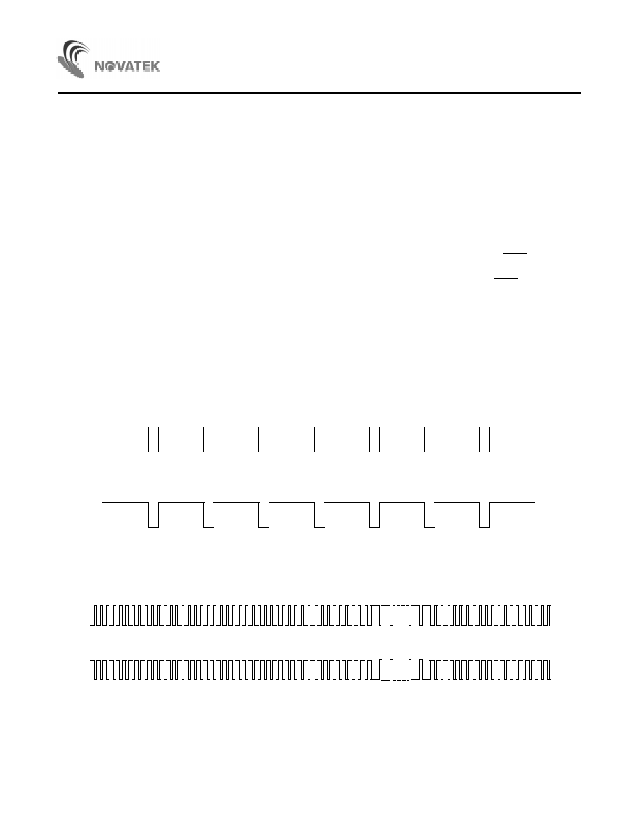
(a) Positive polarity
(b) Negative polarity
Figure 12. Separate H Sync. Waveform
(a) Positive Polarity
(b) Negative Polarity
Figure 13. Composite H Sync. Waveform

NT68P61A
27
VSYNCI
Sampling Clock
8
µ
s
å
å
å
Latch VCNT register
Reset V sync. counter
Start pulse counting
Latch VCNT register
Reset V sync. counter
Start pulse counting
å
å
å
Figure 14. Vsync Counter Operation
HSYNCI
VSYNCI
å
å
å
Latch HCNT register
Reset H sync. counter
Start pulse counting
Latch HCNT register
Reset H sync. counter
Start pulse counting
å
å
å
Figure 15. Hsync Counter Operation Using Vsync Pulse
HSYNCI
å
å
å
HSEL = Low
8.192 ms
å
å
å
Latch HCNT register
Reset H sync. counter
Start pulse counting
Latch HCNT register
Reset H sync. counter
Start pulse counting
Figure 16. Hsync Counter Operation Using 8.192ms Time Interval

NT68P61A
28
Enable
Enable
Enable
Enable
R e s e t
R e s e t
8
µ
s
8.192 ms
HSEL
Control
Logic
V sync.
Latch
H sync.
Latch
S y n c
Separator
H
H P O L I
V P O L I
V
H
H P O L O
V P O L O
H & V
Sync.
Polarity
Detector
H Sync.
Output
Control
F R E E _ R U N
Control
V S Y N C
I N P U T
H S Y N C
I N P U T
H S Y N C O
0
1
1
0
V S Y N C O
H C N T L
H C N T H
Digital
Filter
V C N T L
V C N T H
S / C
V
0
1
V
Schmitt
Trigger
Digital
Filter
Schmitt
Trigger
H sync.
counter
V sync.
counter
V Sync.
Output
Control
S / C
Figure 17. Sync. Processor Block Diagram

NT68P61A
29
13.2. Sync Processor Control Register:
Composite sync: User has to determine whether the
incoming signal is separate sync or composite sync and
set S/ C
& HSEL bit properly. If composite sync signal
is input, after set S/ C
to '0', the sync separator block will
be activated ( please refer figure 18). During Vsync pulse
the Hsync will be inserted Hsync pulse by hardware
circuit and the pulse width of inserted pulse is 2
µ
s fixed.
According to the last Hsync pulse outside the Vsync
pulse duration, the hardware will arrange the interval of
these hardware interpolated pulse. So the insertion of
these Hsync pulse will be continued inside the Vsync
pulse duration no matter what the Hsync pulse originally
exist or not. These inserted Hsync pulse have 0.5
µ
s
phase deviation maximum. The Vsync pulse can be
extracted by hardware from composite signal, and the
output of Vsync signal delay time will be limited bellow
20ns. For inserting Hsync pulse safely, the extracted
Vsync pulse will be widen about 9
µ
s. Because evenly
putting the Hsync pulse, the last inserted Hsync pulse
will have different frequency from original ones.
System will not implement this insertion function, user
must clear INSEN
bit in the MD_CON control register to
activate this function.
After reset, the HSEL , S/ C
& INSEN
bits default value
is HIGH and clear the VCNT | HCNT counter latches to
zero.
Polarity: The detection of Hsync or Vsync polarity is
achieved by hardware circuits sample the sync signal's
voltage level periodically. The user can read HPOLI &
VPOLI bit in HVCON register, from which bit = '1'
representing positive polarity and '0', negative polarity.
The user can read HSYNCI and VSYNCI bit in HVCON
register to detect H & V sync input signal. The user can
control the polarity of H & V sync output signal by
writing the appropriate data to the HPOLO and VPOLO
bits in the HVCON register, '1' represents positive
polarity and '0', negative polarity.
Sync output: In pin assignment, VSYNCO & HSYNCO
represent Vsync & Hsync output which are shared with
P06 & P07 respectively. If set ENV
& ENH
to '0' in
SYNCON register, P06 & P07 will act as VSYNCO &
HSYNCO pin. When input sync is separate signal, the
V/HSYNCO will output the same signal as input sync
signal without delay. But if input sync is composite
signal, the VSYNCO signal will have a delay time of
about 4
µ
s to 8
µ
s. The HSYNCO has no delay output and
still has Vsync pulse among Hsync pulse (i.e. the signal
on HSYNCI pin directly output to HSYNCO pin.)
Free run signal output: The user can set FRUN
to '0' bit
in SYNCON register, then VSYNCO will output 61Hz
Vsync signal and HSYNCO will output 62.5KHz Hsync
signal default (Refer to Figure 20). When FRFREQ
bit
clears to '0', the HSYNCO pin will output 41.7 KHz Hsync
signal. The free run signal has negative or positive
polarity depending on the HPOLO & VPOLO bit setting in
the HV_CON control register, '1' is positive and '0' is
negative polarity. After chip reset, ENV
,
ENH
,
FRFREQ
& FRUN
will enter HIGH state and P06 & P07 will act as
I/O pins.
Half frequency input and output: In this pin assignment,
when ENHALF
sets to
'0' in SYNCON register, the
HALFHO pin will act as an output pin and output half of
input signal in the HALFHI pin with 50% duty
(Refer to Figure 21). If NOHALF
sets
to '0', HALFHO will
output the same signal in the HALFHI pin and user can
control its polarity output of HALFHO by setting
HALFPOL bit, '1' for positive and '0' for negative polarity.
After chip reset, ENHALF
,
NOHALF
& HALFPOL will be
in the HIGH state and P13 & P17 will act as I/O pins.

NT68P61A
30
å
å
å
Composite H sync. waveform (H EOR V)
(1) HSYNCI
å
å
å
(2) HSYNCI
Composite H sync. waveform (H OR V)
å
å
å
2
µ
s
No matter Hsync pulse existing or not,
the output signal of Hsync will be inserted.
H S Y N C O
Inserted Hsync Pulse
V S Y N C O
Original
Hsync Pulse
Original
Hsync Pulse
Widen 9
µ
s
Figure 18. Composite H & V Sync. Processing
NT68P61A
31
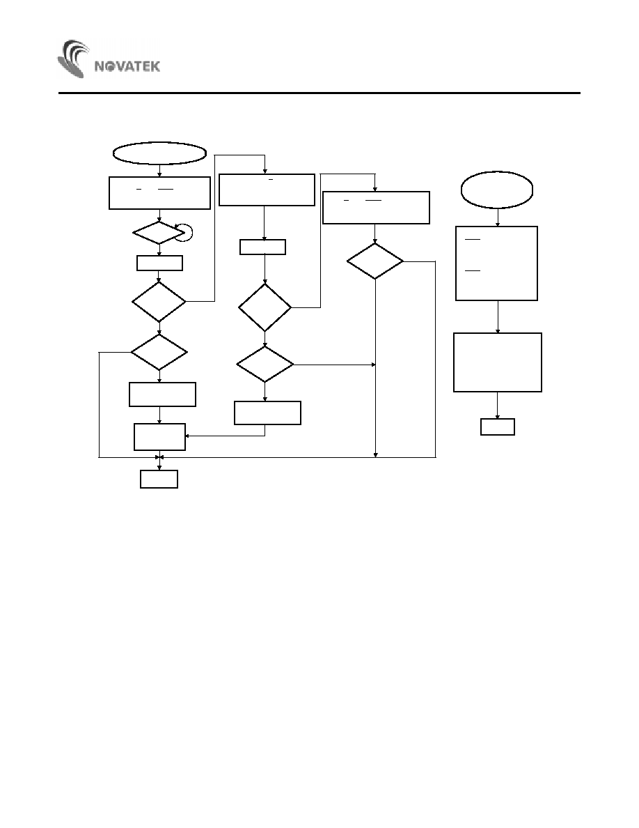
VCNTOV = '1'
?
HCNTH = '00'
?
N o
Y e s
Y e s
N o
R e a d V C N T | H C N T
Counter Register
N O R M A L M o d e
S e p e r a t e S y n c .
Freq.
Calculating
Set S/C = '0'
Clear VCNTOV & HCNTOV
Open INTV & clear INTV flag
VCNTOV = '1'
?
N o
Y e s
Y e s
N o
Return
S T A N D - B Y M o d e
Off Mode
W o r n g M o d e
Y e s
N o
Suspend Mode
Return
Freq.
Calculating
1. Extract HCNTL/H 12 bit data
2. 12 bit data * Vsync. freq.
= Hsync. freq.
3. Its reciprocal
is Hsync. time duration.
1. Extract VCNTL/H 12 bit data
2. HSEL = '1'
12 bit data X 8
µ
s
= Vsync. time duration
3. Its reciprocal
is Vsync. freq.
4. HSEL = '0'
12 bit data X 8.192ms
= Vsync. freq.
Set S/C = '1' & HSEL = '0'
C l e a r V C N T O V & H C N T O V D e l a y 1 0 m s
N O R M A L M o d e
C o m p o s i t e S y n c .
HCNTH ='00'
?
HCNTH = '00'
?
S y n c . M o d e
P r o c e s s i n g
INTV ?
N o
Y e s
D e l a y 6 0 m s
D e l a y 3 1 m s
R e a d V C N T | H C N T
Counter Register
System Default:
Open INTV & clear INTV flag
S/C = '1' & HSEL = '1'
Figure 19. H & V Sync. Software Control Flowchart (for reference only)
NT68P61A
32
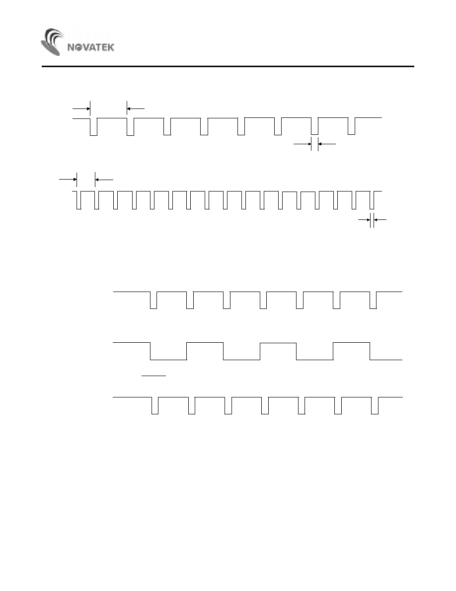
(a) Free run output Vsync. signal
6 1 H z
(1) 62.5KHz
(2) 41.7KHz
Pulse width 64
µ
s
(b) Option 2 of free run output Hsync. signal
Pulse width 1
µ
s
Figure 20. Free Running Sync. Waveform
H A L F H I
HALFHO: Half freq. output signal (50% duty)
HALFHO output signal when NOHALF bit clears to LOW
(the same signal as in the HALFHI pin)
Figure 21. Half Freq. Sync. Waveform

NT68P61A
33
13.3. Power Saving Mode Detect:
The VIDEO mode is listed below. Power saving is from mode 2 to mode 4. All modes can be detected by setting the
control register properly. Refer to Figure 15 control flow chart for software reference.
Mode
H-Sync
V-Sync
(1) Normal
Active
Active
(2) Stand by
Inactive
Active
(3) Suspend
Active
Inactive
(4) Off
Inactive
Inactive
Control bit description:
Addr.
Register
INIT
Bit7
Bit6
Bit5
Bit4
Bit3
Bit2
Bit1
Bit0
$0005
MD CON
07H
-
-
-
-
-
-
-
-
-
INSEN
-
HSEL
S/ C
S/ C
MD1/
2
MD1/
2
R
W
$0006
HV CON
2FH
HCNTOV
VCNTOV
HSYNCI
VSYNCI
HPOLI
VPOLI
HPOLO
VPOLO
R
W
$0007
HCNT L
00H
HCL7
HCL6
HCL5
HCL4
HCL3
HCL2
HCL1
HCL0
R
$0008
HCNT H
00H
-
-
-
-
HCH3
HCH2
HCH1
HCH0
R
$0009
VCNT L
00H
VCL7
VCL6
VCL5
VCL4
VCL3
VCL2
VCL1
VCL0
R
$000A
VCNT H
00H
-
-
-
-
VCH3
VCH2
VCH1
VCH0
R
$000B
SYNCON
FFH
NOHALF
ENHALF
-
FRUN
FRFREQ
HALFPOL
ENH
ENV
W
$0011
CLR FLG
00H
CLRHOV
CLRVOV
CLRINTS
CLRINTD
CLRINTA
CLRINTR
CLRINTE
CLRINTV
W
MDCON control register:
S/ C : The SYNC MODE control. If the input of V & H
Sync are separate signals, set this bit to
'1' (system default). If the input is composite
signal, clear this bit. Under the COMPOSITE
mode,
NT68P61A will extract the V Sync form H Sync
signal.
HSEL : When clearing this bit, system will reset
HCNTL|H counter to zero. The number of Hsync
pulse at the 8.192ms interval is obtained.
INSEN
:
User can clear this bit for inserting Hsync pulse
when processing the composite signal. System
will disable this function after reset.
HVCON control register:
HCNTOV: The overflow bit of H Sync. After setting
HSEL
bit
'1' without any input Vsync pulses and
there are more than 4096 Hsync pulses
coming ,this bit will be set. It will keep '1' and
user can clears it by setting CLRHOV bit to '1'
at the CLRFLG control register. After cleared,
the H Sync counter will reset to '0' and start
counting for every Hsync pulse.
VCNTOV: The overflow bit of V Sync. The operation is
the same as HCNTOV. After cleared, the
Vsync counter will reset to '0' and start
counting for every 8
µ
s.
HSYNCI & VSYNCI:User can instantaneously detect
input of H & V Sync pulse at any
time.
HPOLI & VPOLI: The polarity of input H & V Sync pulse
- '1' for positive polarity and '0' for
negative polarity.
HPOLO & VPOLO:To control the output polarity of H & V
Sync pulse - '1' for positive polarity
and '0' for negative polarity.
HCNTL|H & VCNTL|H control registers:
The 12 bits counter for H & V Sync pulse.
SYNCON control register:
ENH
& ENV : Enable the output of H & V Sync. The P06
& P07 will switch to VSYNCO & HSYNCO
output.
FRUN : Open free run signal at the VSYNCO & HSYNCO
output.
FRFREQ
: Select the free run frequency of H Sync
output.
ENHALF : P12 & P13 will switch to HALFHO & HALFHI
pin. The HALFHO will output the half signal at
the HALFHI pin with 50% duty.
NOHALF : User must clear ENHALF
first. The HALFHO
will output the same signal at the HALFHI
pin.
HALFPOL: User must clear ENHALF
first and control
the

NT68P61A
34
polarity at the HALFHO output pin - '1' for
positive polarity and '0' for negative polarity
.
14. BASE TIMER (BT)
The Base Timer is an 8-bit counter whose clock source must be chosen with 1
µ
s or 1ms by setting or clearing the TBS bit
('0' for 1
µ
s and '1' for 1ms). The BT can be enabled/disabled by the ENBT
bit in the BTCON register. When user clearing
this control bit to '0', the BT will start counting, otherwise setting this bit to '1' will stop the counting. After chip is reset, the
TBS and ENBT
bits are set to '1' (the BT is disabled). BT, can be preset by writing BT7 - BT0 to the BT register (write
only) at any time and the BT will start count-up from preset value. When the value reaches FFH, it generates a timer
interrupt if the timer interrupt is enabled. When it reaches the maximum value of FFH, the base timer will wrap around and
begin counting at 00H. The timer interval can be within 256 ms maximum if set TBS to '1'. The timer interval can be within
256
µ
s maximum if set TBS to '0'.
B T 7
T M R I N T
1
µ
s
1 m s
T B S
1
0
B T 6
B T 5
B T 4
B T 3
B T 2
B T 1
B T 0
Control bit description:
Addr.
Register
INIT
Bit7
Bit6
Bit5
Bit4
Bit3
Bit2
Bit1
Bit0
$0016
BT
00H
BT7
BT6
BT5
BT4
BT3
BT2
BT1
BT0
W
$0017
BT CON
03H
-
-
-
-
-
-
TBS
ENBT
W
BT control register :
BT0 - BT7: Preloaded value of the base timer. The timer will count-up from this value.
BTCON control register:
ENBT : When clearing this bit, the base timer will be activated.
TBS: Select the input clock source of base timer - '1' for 1ms and '0' for 1
µ
s.

NT68P61A
35
15. I
2
C Bus Interface: DDC1 & DDC2B Slave Mode
I
2
C bus interface is a two-wire, bi-directional serial bus which provides a simple, efficient way for data communication
between devices. Its structure minimizes the cost of connecting various peripheral devices. In short, the wired-AND
connection of all I
2
C interface to I
2
C bus is the most important structure. Two modes of operation have been implemented
in NT68P61A: UNI-DIRECTIONAL mode (DDC1 mode) and BI-DIRECTIONAL mode (DDC2B mode). If the MD1/ 2
bit is
set to '1', the device will operate in the DDC1 mode, and if the MD 1/ 2
bit is cleared to '0', the device will operate in the
DDC2B mode. All of these I
2
C functions will be activated only when ENDDC
bit clears to '0' (in IISTS register). When I
2
C
bus
function is activated, the P30 & P31 will switch to SCL & SDA pin. System works on the DDC1 mode transmission default.
The SCL pin will remain high and SDA will transfer one bit of data at every rising edge of Vsync pulse.
Shift Register (IIDAT)
clock source
V S Y N C
S D A
S C L
M D 1 / 2
0
1
15.1. DDC1 Bus Interface
Vsync input and SDA pin: In DDC1 data transfer, the
Vsync input pin is used as an input clock for data
transmission and SDA output pin, as serial data line.
This function comprises of two data buffers: one is a
preloaded data buffer for user placing one bit of data in
advance, and one is shift register for system shifting out
one bit of data to the SDA pin. These two data buffer
cooperate properly. Refer to Figure 18. After system
reset, the I
2
C bus interface is in DDC1 mode.
Data transfer: In advance, put one byte transmitted data
into IIDAT register and activate I
2
C bus by setting
ENDDC
bit to '0' and open INTD interrupt source by
setting IEINTD to '1'. On the first 9 rising edge of Vsync,
system will shift out any invalid bit in shift register to
SDA pin to empty shift register. When shift register is
empty and on next rising edge of Vsync, it will load data
in the IIDAT register to internal shift register. At the same
time, NT68P61A will shift out MSB bit and generate an
INTD interrupt to remind user to replace next byte data
into IIDAT register. After eight rising clocks, there are
eight bits shifted out in proper order and the shift register
becomes empty again. At the ninth rising clock, it will
shift the ninth bit (null bit '1') out to SDA. And on the next
rising edge of Vsync clock, system will generate a INTD
interrupt again. NT68P61A will also load new data in the
IIDAT register to internal shift register and shift out one
bit immediately. User must input new data to IIDAT
register properly before the shift register is empty (the
next INTD interrupt).
Vsync clock: In the separate sync signal, the Vsync pulse
is used as a data transfer clock. Its frequency allows
25KHz maximum. If no Vsync input signal is found,
NT68P61A can not transmit any data to SDA pin
regardless what the Vsync has extracted from composite
Hsync signal.
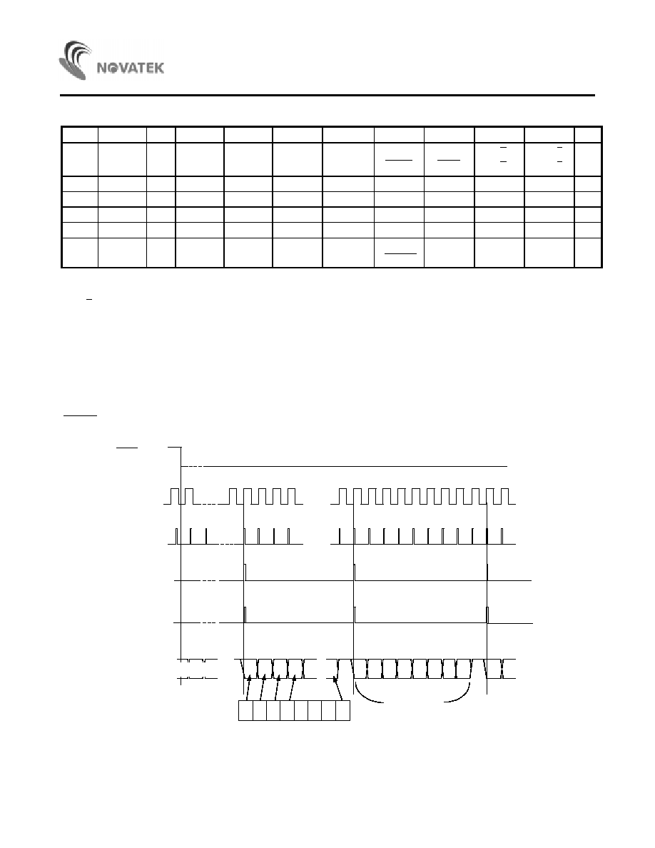
NT68P61A
36
Control bit description:
Addr.
Register
INIT
Bit7
Bit6
Bit5
Bit4
Bit3
Bit2
Bit1
Bit0
$0005
MD CON
07H
-
-
-
-
-
-
-
-
-
INSEN
-
HSEL
S/ C
S/ C
MD1/
2
MD1/
2
R
W
$000F
IEX
00H
-
-
IEINTS
IEINTD
IEINTA
IEINTR
IEINTE
IEINTV
W
$0010
IRQX
00H
-
-
IRQINTS
IRQINTD
IRQINTA
IRQINTR
IRQINTE
IRQINTV
R
$0011
CLR FLG
00H
CLRHOV
CLRVOV
CLRINTS
CLRINTD
CLRINTA
CLRINTR
CLRINTE
CLRINTV
W
$0014
II DAT
00H
SR7
SR6
SR5
SR4
SR3
SR2
SR1
SR0
RW
$0015
II STS
08H
-
-
START
START
STOP
STOP
ENDDC
TRX
RXAK
-
TXAK
R
W
MDCON control register:
MD1/ 2 : Select the DDC mode - '1' for DDC1 and '0' for DDC2B mode. System will be DDC1 mode by default.
When transmission mode is changed form DDC1 to DDC2B, system automatically clears this bit.
IEX control register:
At DDC1 mode, only open INTD interrupt, as well as open INTS interrupt to detect if has changed to DDC2B mode.
II_DAT control register: Data buffer for transmission.
II_STS control register:
ENDDC : When clearing this bit, system will activate DDC transmission. P30 & P31 will switch to SDA & SCL pin.
1
2
3
4
9
1
2
3
4
5
6
7
INTV
8
9
1
2
Vsync Pulse
ENDDC
(in IISTS register)
INTD
8
7
6
8
7
6
5
4
3
2
1
Shift
register
SDA
1
8
7
Null
Bit
5
4
3
1
8
6
2
Null
Bit
å
å
å
5
7
MSB
LSB
Second Byte Data
First Byte Data
Invalid data
User can load next byte data to IIDAT register
Load data in the IIDAT register to shift register
å
å
å
å
å
å
å
å
å
å
å
å
å
å
å
å
å
å
å
å
å
å
å
å
Figure 22. DDC1 Mode Timing Diagram

NT68P61A
37
15.2 DDC2B Slave Mode Bus Interface
The DDC2B I
2
C Bus Interface features are as follows:
- SLAVE mode (NT68P61A addressed by a master
which drive SCL signal)
- Fully compatible with I
2
C bus standard
- Interrupt and generation of acknowledge handled by
user for communication
- Interrupt driven byte by byte data transfer
- Calling address identification interrupt
- Detection of START and STOP signals
Enable I
2
C and INTS: The NT68P61A included the use in
applications requiring storage and serial transmission of
configuration and control information. User can place
address data into IIADR register and set IEINTS to '1' (in
IEX register) in advance. In the DDC1 mode (after
clearing ENDDC
to '0') and when the low level on the
SCL pin occurs, NT68P61A will remind user by
generating a INTS interrupt and switch to DDC2B mode
automatically. When user sets MD1/ 2
to '1' at this time,
the NT68P61A will still proceed with a DDC1
communication. The DDC2B bus consists of two wires,
SCL and SDA; SCL is for the data transmission clock
and SDA is for the data line. Data transfers follow the
format shown in Figure 19. The standard communication
of I
2
C bus protocol includes four parts: a START signal,
slave ADDRESS, transferred data (proceed byte by byte)
and a STOP signal. In the wired-AND connection, any
slow devices can hold the SCL line LOW to force the fast
device into a wait state until the slow device is ready for
the next bit or byte transfer in a type of handshake
procedure.
8
7
6
5
1
8
7
A C K
5
4
3
1
8
6
2
å
å
å
7
å
å
å
1 - 7
S C L
8
9
å
å
å
1 - 7
8
9
å
å
å
1 - 7
8
9
S D A
S T A R T
C O N D I T I O N
S T O P
C O N D I T I O N
A D D R E S S
R / W
A C K
D A T A
A C K
D A T A
A C K
4
å
å
å
I I D A T R e g .
b i t s t r e a m
M S B
M S B
M S B
L S B
L S B
A C K
Figure 23. DDC2B Data Transfer

NT68P61A
38
Start condition: When SCL & SDA lines are in HIGH
state, an external device (master) may initiate
communication by sending a START signal (defined as
SDA from high to low transition while SCL is in high
state). When there is a START condition, NT68P61A will
set the 'START' bit to '1' and user can poll this status bit
to control DDC2B transmission at any time. This bit will
keep '1' until user clears it. After sending a START signal
for DDC2B communication, an external device can
repeatedly send start conditions without sending a STOP
signal to terminate this communication. This is used by
the external device to communicate with another slave or
with the same slave in different mode (READ or WRITE
mode) without releasing the bus.
Address matched and INTA: After the START condition,
a slave address is sent by external device. When I
2
C bus
interface changes to DDC2B mode, NT68P61A will first
act as a receiver to receive this one byte data. This
address data is 7 bits long followed by the eighth bit that
indicates the data transfer direction (R/ W ). When
NT68P61A system receives address data from external
device, it will store if in IIDAT register. System support
'A0' address by default and another one set of DDC2
address for user. When user enable DDC2 function, the
system will compare address data getting from external
device with the default address 'A0' and data in the
$0013 II_ADR control register written by user. Either of
these address matched, the system will generate an
INTA interrupt flag and this DDC2 communication will be
continued. If user sets IEINTA bit to '1' in advanced and
address data matched, the NT68P61A system will
generate a INTA interrupt. Under the address matching
condition, the NT68P61A will send an acknowledgment
to external device. If address data not matched, the
NT68P61A will not generate INTA interrupt and not care
the data change on SDA line in the future.
Data Transmission direction: At INTA interrupt servicing
routine, user must check the LSB of address data in
IIDAT register. According to I
2
C bus protocol, this bit
indicates the DDC2B data transfer direction in later
transmission - a '1' indicates a request for 'READ
MODE' action (external read data from system); a '0'
indicates a 'WRITE MODE' action (external write data to
system). For READ mode and WRITE mode timing
diagram refer to Figure 24 and 25. The data transfer can
be proceeded byte by byte in a direction specified by the
R/ W
bit after a successful slave address is received.
User must set TRX bit in the IISTS register for
NT68P61A transmission mode - '1' for READ mode and
'0' for WRITE mode.
Data validity and transfer: The data on the SDA line mu
be stable during the HIGH period of the clock on the SCL
line. The HIGH and LOW state of the SDA line can only
change when the clock signal on the SCL line is LOW.
Each byte data is eight bits long and one clock pulse for
one bit of data transfer. Data is transferred with the most
significant bit (MSB) first. If a receiver (external device or
NT68P61A) cannot receive another complete byte of
data until it has performed some other function, for
example servicing an internal interrupt, it can hold the
clock line SCL LOW to force the transmitter into a wait
state. Data transfer then continues when the receiver is
ready for another byte of data and release clock line
SCL. Each byte data is followed by an acknowledge bit.
Acknowledge: The acknowledgment will be generated at
ninth clock by whom receive data. In the WRITE mode,
NT68P61A system must respond to this
acknowledgment. After receiving one byte data from
external device, NT68P61A will automatically send an
acknowledgment by pulling SDA line to 'LOW'. In the
READ MODE, external device must respond to this
acknowledgment and at every byte data sent, user can
read RXAK bit in IISTS register to check if external sent
a ACK or not.
The INTD interrupt: After NT68P61A receive the START
condition, it will generate an INTD interrupt at the falling
edge of the ninth clock. User can control the flow of
DDC2B transmission at this INTD interrupt.
The INTD on the WRITE mode: NT68P61A read data
from external device. At INTD interrupt, the SCL will be
hold LOW by NT68P61A. When getting one byte data
from II_DAT register, user can write '00' into II_DAT
register and the SCL will be released. External device
can continue sending next byte data to NT68P61A.
Refer to Figure 24.
The INTD on the READ mode: External device read data
from NT68P61A. At INTD interrupt, the SCL will be hold
LOW by NT68P61A. User can check RXACK bit in the
IISTS register whether external device has sent an ACK
or not after one byte data transfer. If external device has
sent an ACK, the RXACK will be '0' (assume the
acknowledgment is LOW signal). When user puts one
new byte data into II_DAT register, the SCL will be
released for generation of SCL transmission clock. The
next byte data will be shifted out properly. Refer to
Figure 25.
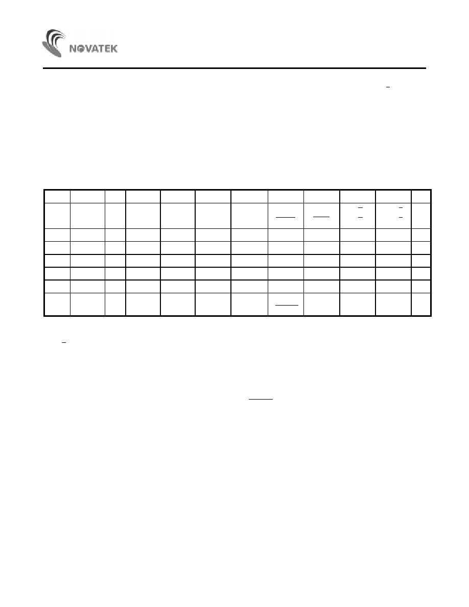
NT68P61A
39
STOP condition: When SCL & SDA lines have been
released (remain in 'HIGH' state), DDC2B data transfer
is always terminated by a STOP condition generated by
external device. A STOP signal is defined as a low to
high transition of SDA while SCL is in HIGH state. When
there is a STOP condition, NT68P61A will set the 'STOP'
bit to '1' and user can poll this status bit to control
DDC2B transmission at any time. This bit keeps '1' until
user clears it. Notice the SCL and SDA lines must
conform to I
2
C bus specifications. (Refer to Figure 26).
Refer to the standard I
2
C bus specification for details.
Changing to DDC1 mode: After an external device
terminates DDC2 transmission, set MDI/ 2
to 1 for
changing to DCC1 mode. When the SCL line has been
released (pulled-up), user can force NT68P61A to DDC1
mode communication at any time. This function is
supporting the 'error' recovery protocol in the VESA DDC
standard Ver 2.0.
Control bit description:
Addr.
Register
INIT
Bit7
Bit6
Bit5
Bit4
Bit3
Bit2
Bit1
Bit0
$0005
MD CON
07H
-
-
-
-
-
-
-
-
-
INSEN
-
HSEL
S/ C
S/ C
MD1/
2
MD1/
2
R
W
$000F
IEX
00H
-
-
IEINTS
IEINTD
IEINTA
IEINTR
IEINTE
IEINTV
W
$0010
IRQX
00H
-
-
IRQINTS
IRQINTD
IRQINTA
IRQINTR
IRQINTE
IRQINTV
R
$0011
CLR FLG
00H
CLRHOV
CLRVOV
CLRINTS
CLRINTD
CLRINTA
CLRINTR
CLRINTE
CLRINTV
W
$0013
II ADR
FFH
AR7
AR6
AR5
AR4
AR3
AR2
AR1
-
W
$0014
II DAT
00H
SR7
SR6
SR5
SR4
SR3
SR2
SR1
SR0
RW
$0015
II STS
08H
-
-
START
START
STOP
STOP
ENDDC
TRX
RXAK
-
R
W
MDCON control register:
MD1/ 2 : Select the DDC mode - '1' for DDC1 and '0' for
DDC2B mode. System will be DDC1 mode by
default.
When transmission mode is changed form
DDC1 to DDC2B, system will automatically
clear
this bit.
IEX control register:
In DDC2 mode, user use INTS, INTA & INTD interrupt
and II_STS control register to control DDC2B
transmission.
II_DAT control register: Data buffer for transmission
II_ADR control register: User can define the address of
DDC2B device. If an external
device sends the same address
data as this control register
(calling NT68P61A), NT68P61A
will generate an INTA interrupt.
II_STS control register:
ENDDC : When clearing this bit, the system will activate
DDC transmission. P30 and P31 will switch to
SDA and SCL pin.
TRX: In the READ mode of DDC2B transmission, user
must set this bit '1'.
RXAK: In the WRITE mode of DDC2B transmission,
after
one byte has been sent out to the SDA line,
there will be an INTD interrupt. At INTD interrupt
service routine, user can check this bit to see if
external device has responded to NT68P61A.

NT68P61A
40
1
0
1
0
0
0
0
0
S C L
S D A
( e x t e r n a l d e v i c e )
D A T A
D A T A
S T A R T
S T O P
I N T S
I N T A
I N T D
S D A
( N T 6 8 P 6 1 A )
A
A
A
R / W
w a i t
w a i t
w a i t
w a i t
(b) WRITE_Mode Timing Diagram
(a) WRITE_Mode Data Format
D A T A
0
A
A
A
D a t a t r a n s f e r r e d
f r o m e x t e r n a l d e v i c e
F r o m e x t e r n a l d e v i c e t o N T 6 8 P 6 1 A
F r o m N T 6 8 P 6 1 A t o e x t e r n a l d e v i c e
A = a c k n o w l e d g e
S = S T A R T
P = S T O P
N T 6 8 P 6 1 A A d d r e s s
S
R / W
D A T A
P
Figure 24. DDC2B Write_Mode Spec.
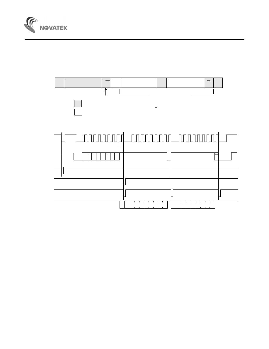
NT68P61A
41
1
0
1
0
0
0
0
1
S C L
S D A
( e x t e r n a l d e v i c e )
D A T A
D A T A
S T A R T
S T O P
I N T S
I N T A
I N T D
S D A
( N T 6 8 P 6 1 A )
A
R / W
w a i t
w a i t
w a i t
w a i t
(b) READ_Mode Timing Diagram
(a) Read_Mode Data Format
D A T A
P
1
A
A
D a t a t r a n s f e r r e d
f r o m e x t e r n a l d e v i c e
F r o m e x t e r n a l d e v i c e t o N T 6 8 P 6 1 A
F r o m N T 6 8 P 6 1 A t o e x t e r n a l d e v i c e
A = a c k n o w l e d g e
A = n o a c k n o w l e d g e
Ô ¾ ÔÕÂÓÕ
Ñ ¾ ÔÕÐÑ
Â
Â
S
N T 6 8 P 6 1 A A d d r e s s
R / W
D A T A
A
Figure 25. DDC2B Read_Mode Spec.
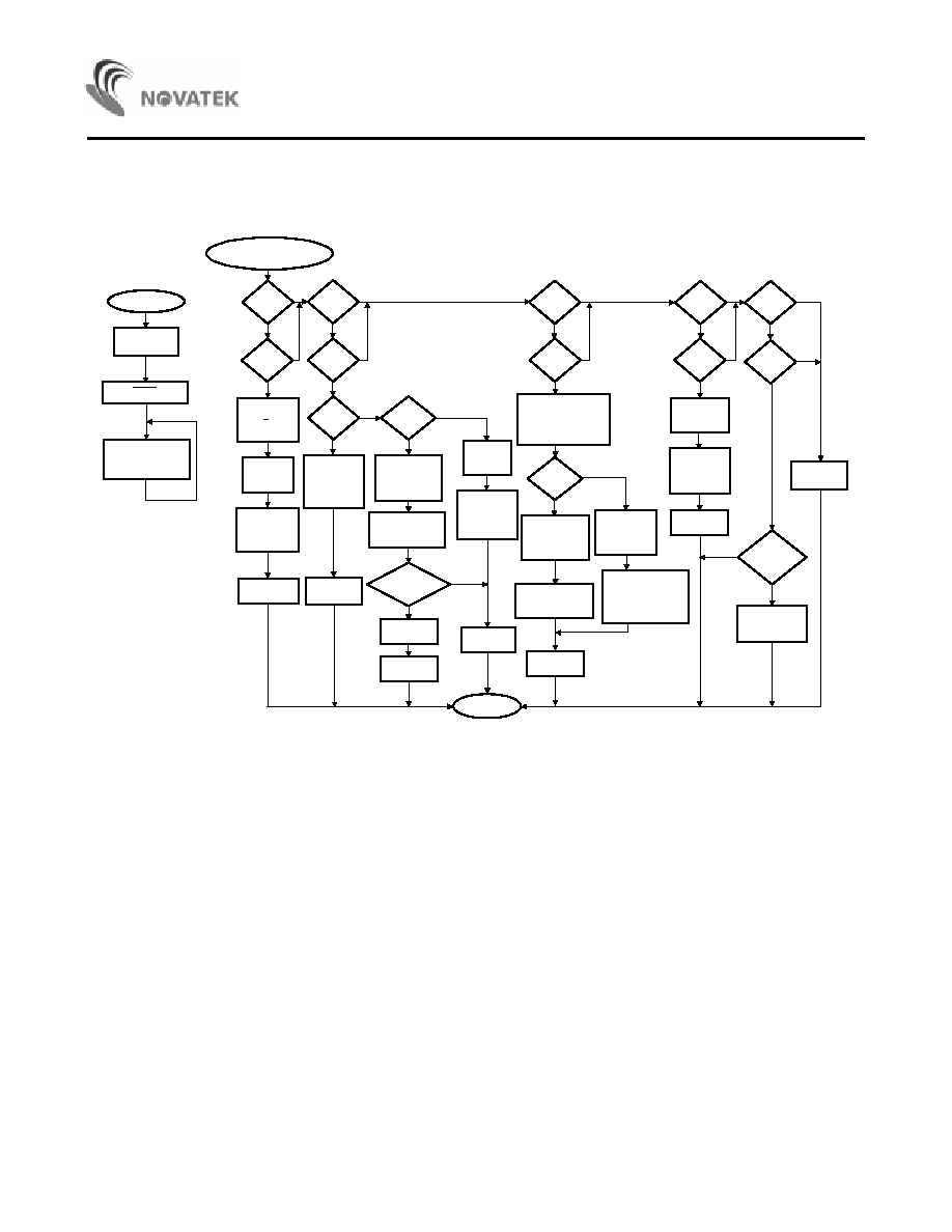
NT68P61A
42
Open
INTV & INTS
Wait Interrupt
or
Doing something
Main Program
Interrupt Service Routine
Polling
INTS ?
DDC2
yes
No
Open
INTA & INTR
Change To
DDC2 Mode
MD 1/2 = 0
(Auto Switch)
Put Addr.
Into
IIADR Reg.
INTV ?
Open
INTS & INTD
DDC1
yes
No
Reset EDID
Buffer Index
Put One Byte
Data Into
IIDAT Reg.
Change To
DDC1 Mode
MD_CON = 1
No
Return
yes
DDC2 Operate
Over ?
yes
Open
INTA & INTV
DDC1
Transfer ?
yes
yes
No
No
DDC2B
Write_Mode
Operation
?
From EDID
Buffer Index
Put One Byte
Data Into
IIDAT Reg.
Read One Byte
Data From
IIDAT Reg.
To Set EDID
Buffer Index
Write '00'
To IIDAT
For releasing SCL
INTA ?
yes
Open
INTA & INTD
Reset EDID Buffer Index
From IIDAT Reg.
LSB
To Decide
Write/Read Mode
yes
No
Put First Byte
Data Into
IIDAT Reg.
For releaseing SCL
& For Transfer data
No
Other INT.
Service
No
From EDID
Buffer Index
Put One Byte
Data Into
IIDAT Reg.
yes
yes
yes
yes
No
No
No
No
Need
Polling
INTS ?
Need
Polling
INTA ?
Open
INTA & INTD
Need
Polling
INTD ?
INTD ?
Write '00'
To IIDAT
For releasing SCL
Setting IISTS:
TRX = 0
(Recv. Mode)
Setting IISTS:
TRX = 0
(Recv. Mode)
DDC2B
Read_Mode
Operation
DDC2B
Write_Mode
Operation
?
Setting IISTS:
TRX = 1
(Trans. Mode)
Need
Polling
INTV ?
Set ENDDC = 0
Open
INTS & INTD
Reset EDID
Buffer Index
Need
Polling
INTR ?
INTR ?
DDC2 Idle
For 2 Sec. ?
Return To
DDC1 Mode
Open INTV
No
No
yes
yes
yes
NO
Figure 26. DDC1/2B Software Flow Chart
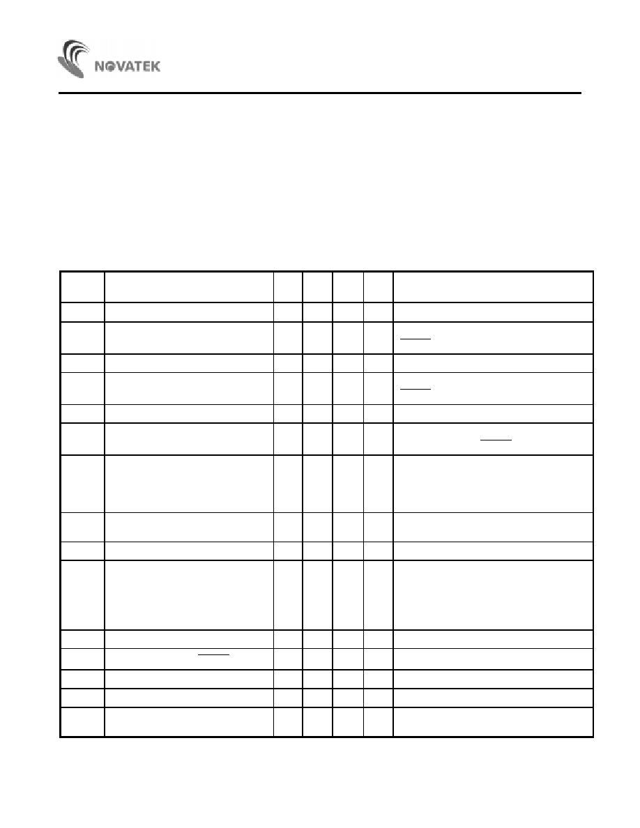
NT68P61A
43
Absolute Maximum Ratings*
DC Supply Voltage V
DD
- V
SS
. . . . . . . . . . . .-0.3V to 7V
Input Voltage . . . . . . . . . . . . . . GND -0.2V to V
CC
+0.2V
Operating Temperature . . . . . . . . . . . . . . . . 0
°
C to
+70
°
C
Storage Temperature . . . . . . . . . . . . . . . -50
°
C to
+125
°
C
*Comments
Stresses above those listed under "Absolute Maximum
Ratings" may cause permanent damage to this device.
These are stress ratings only. Functional operation of
this device at these or any other conditions above those
indicated in the operational sections of this specification
is not implied or intended. Exposed to the absolute
maximum rating conditions for extended periods may
affect device reliability.
DC Electrical Characteristics
(V
DD
= 5V, T
A
= 25
°
C, oscillator freq. = 8MHz, unless otherwise specified)
Symbol
Parameter
Min
.
Typ.
Max
.
Unit
Conditions
I
DD
Operating Current
20
mA
No loading
VIH1
Input High Voltage
2
V
P00 - P07, P10-P16, P20-P27, P30, P31,
RESET
,
VSYNCI, HSYNCI, HALFHI, INTE
VIH2
Input High Voltage
3
V
SCL, SDA pins
VIL1
Input Low Voltage
0.8
V
P00 - P07, P10 - P16, P20 - P27, P30, P31,
RESET
,
VSYNCI, HSYNCI, HALFHI, INTE
VIL2
Input Low Voltage
1.5
V
SCL, SDA pins
IIH
Input High Current
-200
-350
µ
A
P00 - P07, P10 - P16 ,P20 -P27, VSYNCI,
HSYNCI, HALFHI, RESET
(VIH = 2.4V)
VOH1
Output High Voltage
2.4
V
P00 - P07, P10 - P15 (I
OH
= -100
µ
A)
VSYNCO, HSYNCO (I
OH
= -4mA)
HALFHO (I
OH
= -4mA)
P20-P27 (I
OH
= -10mA)
VOH2
Output High Voltage (DAC8 -
DAC13)
5
V
external applied voltage
VOH3
Output High Voltage (DAC0 - DAC7)
12
V
external applied voltage
VOL
Output Low Voltage
0.4
V
P00 - P07, P10 - P15, DAC0 - 13 (I
OL
=
4mA) SCL/P30, SDA/P31 (I
OL
= 5mA)
VSYNCO, HSYNCO (I
OL
= 4mA)
HALFHO (I
OL
= 4mA)
P20 - P27 (I
OL
= 10mA)
VLVR
Low Voltage Threshold
4.0
V
ROL
Pull Down Resistor ( RESET
)
25K
50K
75K
ROH1
Pull Up Resistor (INTE)
11K
22K
33K
ROH2
Pull Up Resistor (PORT0 & PORT1)
11K
22K
33K
ROH3
Pull Up Resistor (HSYNCI &
VSYNCI)
11K
22K
33K

NT68P61A
44
AC Electrical Characteristics
(V
DD
= 5V, T
A
= 25
°
C, oscillator freq. = 8MHz, unless otherwise specified)
Symbol
Parameter
Min.
Typ.
Max.
Unit
Condition
Fsys
System Clock
8
MHz
t
CNVT
A/D Conversion Time
375
µ
s
Voffset
A/D Converter Offset Error
39
mV
Vin = 2V for A/D converter
Vlinear
A/D Input Dynamic Range of Linearity
Conversion
0.3
0.7
V
DD
tinst
The Inserted Hsync Pulse Width
2
µ
s
Composite sync
(Refer Figure 18)
tdev
The time deviation at the end edge of
inserted Hsync pulse
250
ns
Composite mode &
insertion function activated
t
RESET
Reset Pulse Width Low
2
t
CYCLE
t
CYCLE
= 2/Fsys
Fvsync
Vsync Input Frequency
32
25K
Hz
t
VSYNC
= 1/Fvsync
t
VPW
Vsync Input Pulse Width
8
300
µ
s
Fhsync
Hsync Input Frequency
30
120
KHz
t
HSYNC
= 1/Fhsync
t
HPW1
Hsync Input Pulse Width High
0.5
7
µ
s
t
HPW2
Hsync Input Pulse Width Low
8
µ
s
Composite sync
t
ERROR1
Counting Deviation of Base Timer
1
µ
s
1
µ
s clock source
t
ERROR2
Counting Deviation of Base Timer
1
ms
1ms clock source

NT68P61A
45
DDC1 Mode
Symbol
Parameter
Min.
Typ.
Max.
Unit
Condition
t
VPW
Vsync High Time
0.5
300
us
Fvsync
Vsync Input Frequency
32
25K
Hz
t
VSYNC
= 1/Fvsync
t
DD
Data Valid
200
500
ns
t
MODE
Time for Transition to DDC2B
Mode
500
ns
Bit 0
Null Bit
Bit 7
Bit 6
S C L
S D A
V S Y N C
t
MODE
t
DD
t
VPW
Composite
Hsync Input
Extracted
Vsync Output
(no loading)
å
å
å
t
HPW1
t
HPW2

NT68P61A
46
DDC2B Mode
Symbol
Parameter
Min.
Typ.
Max.
Unit
fSCL
SCL Clock Frequency
100
KHz
t
BUF
Bus Free Between a STOP and START Condition
4.7
µ
s
t
HD
; STA
Hold Time for START Condition
4
µ
s
t
LOW
LOW Period of the SCL Clock
4.7
µ
s
t
HIGH
HIGH Period of the SCL Clock
4
µ
s
t
SU
; STA
Set-up Time for a Repeated START Condition
4.7
µ
s
t
HD
; DAT
Data Hold Time
300
ns
t
SU
; DAT
Data Set-up Time
300
ns
t
R
Rise Time of Both SDA and SCL Signals
1
µ
s
t
F
Fall Time of Both SDA and SCL Signals
300
ns
t
SU
; STO
Set-up Time for STOP Condition
4
µ
s
S C L
S D A
t
BUF
t
HD
; STA
t
SU
; DAT
t
HIGH
t
R
t
F
t
HD
; DAT
t
LOW
S T O P
S T A R T
t
SU
; S T A
t
HD
; ST A
S T O P
t
SU
; ST O
S T A R T

NT68P61A
47
Ordering Information
Part No.
Package
NT68P61A
40L DIP

NT68P61A
48
Package Information
DIP 40L Outline Dimensions
unit: inches/mm
1
2 1
4 0
E
1
S
A
2
A
L
E
e
A
D
C
B
1
B
A
1
B a s e P l a n e
S e a t i n g P l a n e
2 0
e
1
Symbol
Dimensions in inches
Dimensions in mm
A
0.210 Max.
5.33 Max.
A
1
0.010 Min.
0.25 Min.
A
2
0.155±0.010
3.94±0.25
B
0.018 +0.004
0.46 +0.10
-0.002
-0.05
B
1
0.050 +0.004
1.27 +0.10
-0.002
-0.05
C
0.010 +0.004
0.25 +0.10
-0.002
-0.05
D
2.055 Typ. (2.075 Max.)
52.20 Typ. (52.71 Max.)
E
0.600±0.010
15.24±0.25
E
1
0.550 Typ. (0.562 Max.)
13.97 Typ. (14.27 Max.)
e
1
0.100±0.010
2.54±0.25
L
0.130±0.010
3.30±0.25
0
°
~ 15
°
0
°
~ 15
°
e
A
0.655±0.035
16.64±0.89
S
0.093 Max.
2.36 Max.
Notes:
1. The maximum value of dimension D includes end flash.
2. Dimension E
1
does not include resin fins.
3. Dimension S includes end flash.