
NT68P62-01
8-Bit Microcontroller for Monitor (32K OTP ROM Type)
1
V2.2
Features
n
Operating voltage range: 4.5V to 5.5V
n
CMOS technology for low power consumption
n
6502 8-bit CMOS CPU core
n
8 MHz operation frequency
n
32K bytes of OTP (one time programming) ROM
n
512 bytes of RAM
n
One 8-bit base timer
n
13 channels of 8-bit PWM outputs with 5V open drain
n
4 channel A/D converters with 6-bit resolution
n
25 bi-directional I/O port pins (8 dedicated I/O pins)
n
Hsync/vsync signals processor for separate &
composite signal, including hardware sync signals
polarity detection and freq. counters with 2 sets of
Hsync counting interval
n
Hsync/Vsync polarity controlled output, 5 selectable
free run output signals and self-test patterns, auto-
mute function, half freq. I/O function
n
Two built-in I
2
C bus interfaces support VESA
DDC1/2B+
n
Two layers of interrupt management
NMI interrupt sources
- INTE0 (External INT with selectable edge trigger)
- INTMUTE (Auto Mute Activated)
IRQ interrupt sources
- INTS0/1 (SCL Go-low INT)
- INTA0/1 (Slave Address Matched INT)
- INTTX0/1 (Shift Register INT)
- INTRX0/1 (Shift Register INT)
- INTNAK0/1 (No Acknowledge)
- INTSTOP0/1 (Stop Condition Occurred INT)
- INTE1 (External INT with Selectable Edge Trigger)
- INTV (VSYNC INT)
- INTMR (Base Timer INT)
- INTADC (AD Conversion Done INT)
n
Hardware watch-dog timer function
n
40-pin P-DIP and 42-pin S-DIP packages
General Description
The NT68P62 is a new generation of monitor
�
C for auto-
sync and digital control applications. Particularly, this chip
supports various and efficient functions to allow users to
easily develop USB monitors. It contains the 6502 8-bit
CPU core, 512 bytes of RAM used as working RAM and
stack area, 32K bytes of OTP ROM, 13-channel of 8-bit
PWM D/A converters, 4-channel A/D converters for keys
detection which can save I/O pins, one 8-bit pre-loadable
base timer, internal Hsync and Vsync signals processor,
and a watch-dog timer which prevents the system from
abnormal operation and two I
2
C bus interface. The user
can store EDID data in the 128 bytes of RAM for DDC1/2B,
so that user can reduce a dedicated EEPROM for EDID.
And Half frequency output function can save external one-
shot circuit. All of these designs are committed to offer our
user saving component cost. The 42 pin S-DIP IC provides
two additional I/O pins � port40 & port41, Part number
NT68P62U represents the S-DIP IC. For future reference,
port40 & port42 is only available for the 42 pin S-DIP IC.

NT68P62-01
2
Pin Configurations
40-Pin P-DIP
[PGM] DAC2
DAC1/ADC3
[OE] DAC0/ADC2
[DB7] P27
[VPP] RESET
V
DD
GND
OSCO
OSCI
[CE] P14/PATTERN
[A10] P12/HALFO
[A9] P11/ADC1
[A8] P10/ADC0
P20 [DB0]
P07/HSYNCO [A7]
P31/SCL0 [A13]
DAC4/SCL1 [MODE1]
DAC3 [MODE0]
HSYNCI
VSYNCI/INTV [A14]
NT68P62
1
2
3
4
5
6
7
8
9
10
11
12
13
14
15
16
25
26
27
28
29
30
31
32
33
34
35
36
37
38
39
40
P15/INTE0
[A11] P13/HALFI
P16/INTE1
17
18
19
20
24
23
22
21
DAC5/SDA1 [MODE2]
DAC6 [RESET]
CREG
P21 [DB1]
P22 [DB2]
P06/VSYNCO [A6]
P05/DAC12 [A5]
P04/DAC11 [A4]
P03/DAC10 [A3]
P02/DAC9 [A2]
P01/DAC8 [A1]
P00/DAC7 [A0]
P30/SDA0 [A12]
[DB6] P26
[DB5] P25
[DB4] P24
[DB3] P23
* [ ]: OTP Mode
42-Pin S-DIP
[PGM] DAC2
DAC1/ADC3
[OE] DAC0/ADC2
[VPP] RESET
V
DD
P40
GND
OSCO
OSCI
P15/INTE0
[A11] P13/HALFI
[A9] P11/ADC1
[A8] P10/ADC0
P00/DAC7 [A0]
P16/INTE1
P01/DAC8 [A1]
P02/DAC9 [A2]
P03/DAC10 [A3]
P04/DAC11 [A4]
P06/VSYNCO [A6]
P07/HSYNCO [A7]
DAC6 [RESET]
P41
DAC5/SDA1 [MODE2]
DAC4/SCL1 [MODE1]
DAC3 [MODE0]
HSYNCI
VSYNCI/INTV [A14]
CREG
NT68P62U
1
2
3
4
5
6
7
8
9
10
11
12
13
14
15
16
27
28
29
30
31
32
33
34
35
36
37
38
39
40
41
42
[CE] P14/PATTERN
[A10] P12/HALFO
[DB7] P27
[DB6] P26
[DB5] P25
[DB4] P24
[DB3] P23
17
18
19
20
21
P05/DAC12 [A5]
P31/SCL0 [A13]
P30/SDA0 [A12]
P20 [DB0]
P21 [DB1]
P22 [DB2]
26
25
24
23
22
* [ ]: OTP Mode
Block Diagram
Timing Generator
CPU core
6502
Interrupt
Controller
H/V Sync Signals
Processor
SRAM + STACK
512 Bytes
Watch Dog Timer
PWM DACs
I/O Ports
OSCI
OSCO
V
DD
GND
HSYNCI
INTE0/1
SCL0
SDA0
DAC0 - DAC7
P00 - P07
P10 - P16
P30 - P31
VSYNCO
A/D Converter
ADC0 - ADC3
8-Bit Base Timer
P40 - P41
IIC BUS
P20 - P27
HSYNCO
HALFI
HALFO
DAC8 - DAC12
VSYNCI/INTV
OTP Program ROM
32K Bytes
PATTERN
SCL1
SDA1
Voltage
Regulator
CREG

NT68P62-01
3
Pin Description
Pin No.
40 Pin
42 Pin
Designation
Reset Init.
I/O
Description
1
1
DAC2
[ PGM ]
O
[ I ]
Open drain 5V, D/A converter output 2
[OTP ROM program control]
2
2
DAC1/ADC3
DAC1
O
Open drain 5V, D/A converter output 1, shared with A/D
converter channel 3 input
3
3
DAC0/ADC2
[ OE ]
DAC0
O
Open drain 5V, D/A converter output 0, shared with A/D
converter channel 2 input
[OTP ROM program output enable]
4
4
RESET
[ VPP ]
I
[ P ]
Schmitt Trigger input pin, low active reset with internal
pulled down 50K
register *
[OTP ROM program supply voltage]
5
5
V
DD
P
Power
6
7
GND
P
Ground
7
8
OSCO
O
Crystal OSC output
8
9
OSCI
I
Crystal OSC input
9
10
P15/INTE0
I/O
Bi-directional I/O pin with internal pulled up 22K
register,
shared with input pin of external interrupt source0 (NMI),
with schmitt trigger, selectable triggered, and internal pulled
up 22K
register
10
11
P14/PATTERN
[ A15/CE ]
I/O
[ I ]
Bi-directional I/O pin with internal pulled up 22K
register,
shared with the output of self test pattern
[ OTP ROM program address buffer & chip enable ]
11
12
P13/HALFI
[ A11 ]
P13
I/O
[ I ]
Bi-directional I/O pin with internal pulled up 22K
register,
shared with half hsync input, shared with A/D converter
channel 3 input
[ OTP ROM program address buffer ]
12
13
P12/HALFO
[ A10 ]
P12
I/O
[ I ]
Bi-directional I/O pin with internal pulled up 22K
register,
shared with half hsync output
[ OTP ROM program address buffer ]
13
14
P11/ADC1
[ A9 ]
P11
I/O
[ I ]
Bi-directional I/O pin with internal pulled up 22K
register,
shared with A/D converter channel 1 input
[ OTP ROM program address buffer ]
14
15
P10/ADC0
[ A8 ]
P10
I/O
[ I ]
Bi-directional I/O pin with internal pulled up 22K
register,
shared with A/D converter channel 0 input
[ OTP ROM program address buffer ]
15
16
P16/INTE1
P16
I/O
Bi-directional I/O pin with internal pulled up 22K
register,
shared with input pin of external interrupt source1, with
Schmitt Trigger, selectable triggered, and an internal pulled
up 22K
register

NT68P62-01
4
Pin Description (continued)
Pin No.
40 Pin
42 Pin
Designation
Reset Init.
I/O
Description
16 - 23
17 - 24
P27 � P20
[ DB7 ] � [ DB0]
I/O
[ I/O ]
Bi-directional I/O pin, push-pull structure with high current
drive/sink capability
[ OTP ROM program data buffer ]
24
25
P30/SDA0
[ A12 ]
P30
I/O
[ I ]
Open drain 5V bi-directional I/O pin P30, shared with SDA0
pin of I
2
C bus Schmitt Trigger buffer
[ OTP ROM program address buffer ]
25
26
P31/SCL0
[ A13 ]
P31
I/O
[ I ]
Open drain 5V bi-directional I/O pin P31, shared with SCL0
pin of I
2
c bus Schmitt Trigger buffer
[ OTP ROM program address buffer ]
26
27
P00/DAC7
[ A0 ]
P00
I/O
[ I ]
Bi-directional I/O pin with internal pulled up 22K
register,
shared with open drain 5V D/A converter output 8
[ OTP ROM program address buffer ]
27
28
P01/DAC8
[ A1 ]
P01
I/O
[ I ]
Bi-directional I/O pin with internal pulled up 22K
register,
shared with open drain 5V D/A converter output 9
[ OTP ROM program address buffer ]
28
29
P02/DAC9
[ A2 ]
P02
I/O
[ I ]
Bi-directional I/O pin with internal pulled up 22K
register,
shared with open drain 5V D/A converter output 10
[ OTP ROM program address buffer ]
29
30
P03/DAC10
[ A3 ]
P03
I/O
[ I ]
Bi-directional I/O pin with internal pulled up 22K
register,
shared with open drain 5V D/A converter output 11
[ OTP ROM program address buffer ]
30
31
P04/DAC11
[ A4 ]
P04
I/O
[ I ]
Bi-directional I/O pin with internal pulled up 22K
register,
shared with open drain 5V D/A converter output 12
[ OTP ROM program address buffer ]
31
32
P05/DAC12
[ A5 ]
P05
I/O
[ I ]
Bi-directional I/O pin with internal pulled up 22K
register,
shared with open drain 5V D/A converter output 13
[ OTP ROM program address buffer ]
32
33
P06/VSYNCO
[ A6 ]
P06
I/O
[ I ]
Bi-directional I/O pin with internal pulled up 22K
register,
shared with vsync out
[ OTP ROM program address buffer ]
33
34
P07/HSYNCO
[ A7 ]
P07
I/O
[ I ]
Bi-directional I/O pin with internal pulled up 22K
register,
shared with hsync out
[ OTP ROM program address buffer ]
34
35
CREG
O
On chip voltage regulator output, external regulating
cap.(10�F ~ 100�F) should be connected here
35
36
DAC6
[ RESET ]
O
[ I ]
Open drain 5V, D/A converter output 6
[ OTP ROM reset ]
36
38
DAC5/SDA1
[ MODE2 ]
O
[ I ]
Open drain 5V, D/A converter output 5, shared with open
drain SDA1 line of I
2
C bus, Schmitt Trigger buffer
[ OTP ROM mode select ]

NT68P62-01
5
Pin Description (continued)
Pin No.
Designation
Reset Init.
I/O
Description
40 Pin
42 Pin
37
39
DAC4/SCL1
[ MODE1 ]
O
[ I ]
Open drain 5V, D/A converter output 4, shared with open
drain SCL1 line of I
2
C bus, Schmitt Trigger buffer
[ OTP ROM mode select ]
38
40
DAC3
[ MODE0 ]
O
[ I ]
Open drain 5V, D/A converter output 3
[ OTP ROM mode select ]
39
41
HSYNCI
I
Debouncing & Schmitt Trigger input pin for video horizontal
sync signal, internal pull high, shared with composite sync
input
40
42
VSYNCI/INTV
[ A14 ]
VSYNCI
I
[ I ]
Debouncing & Schmitt trigger input pin for video vertical
sync signal, internal pull high, shared with input pin of
external interrupt source intv with Schmitt Trigger,
selectable triggered, and internal pulled up 22K
register
[ OTP ROM program address buffer ]
-
6
P40
I/O
Bi-directional I/O pin with internal pulled up 22K
register,
only 42 pin S-DIP available
-
37
P41
I/O
Bi-directional I/O pin with internal pulled up 22K
register,
only 42 pin S-DIP available
* This RESET pin must be pulled high by external pulled-up register (5K
suggestion), or it will remain in low voltage to
continually rest system.

NT68P62-01
6
Functional Description
1. 6502 CPU
The 6502 is an 8-bit CPU that provides 56 instructions, decimal and binary arithmetic, thirteen addressing modes, true
indexing capability, programmable stack pointer and variable length stack, a wide selection of addressable memory ranges,
and interrupt input options.
The CPU clock cycle is 4MHz (8MHz system clock divided by 2). Please refer to the 6502 data sheet for more detailed
information.
Accumnlator A
Index Register Y
0
7
7
Index Register X
7
0
0
Stack Pointer SP
0
Status Register P
0
7
Carry
Zero
IRQ Disable
Decimal Mode
BRK Command
Overflow
Negative
Figure 1.1. The 6502 CPU Registers and Status Flags
7
Program Counter PCH
8
15
7
0
PCL
1=TRUE
1=Result ZERO
1=DISABLE
1=TRUE
1=NEG
1=TRUE
1=BRK
N
V
C
Z
I
D
B
NT68P62-01
7
2. Instruction Set List
Instruction Code
Meaning
Operation
ADC
Add with carry
A + M + C
A, C
AND
Logical AND
A
�
M
A
ASL
Shift left one bit
C
M7 ... M0
0
BCC
Branch if carry clears
Branch on C
0
BCS
Branch if carry sets
Branch on C
1
BEQ
Branch if equal to zero
Branch on Z
1
BIT
Bit test
A
�
M, M7
N, M6
V
BMI
Branch if minus
Branch on N
1
BNE
Branch if not equal to zero
Branch on Z
0
BPL
Branch if plus
Branch on N
0
BRK
Break
Forced Interrupt PC+2
PC
BVC
Branch if overflow clears
Branch on V
0
BVS
Branch if overflow sets
Branch on V
1
CLC
Clear carry
0
C
CLD
Clear decimal mode
0
D
CLI
Clear interrupt disable bit
0
I
CLV
Clear overflow
0
V
CMP
Compare Accumulator to memory
A
M
CPX
Compare with index register X
X
M
CPY
Compare with index register Y
Y
M
DEC
Decrement memory by one
M
1
M
DEX
Decrement index X by one
X
1
X
DEY
Decrement index Y by one
Y
1
Y
EOR
Logical exclusive-OR
A
M
A
INC
Increment memory by one
M + 1
M
INX
Increment index X by one
X + 1
X
INY
Increment index Y by one
Y + 1
Y
NT68P62-01
8
Instruction Set List (continued)
Instruction Code
Meaning
Operation
JMP
Jump to new location
(PC+1)
PCL, (PC+2)
PCH
JSR
Jump to subroutine
PC+2
, (PC+1)
PCL, (PC+2)
PCH
LDA
Load accumulator with memory
M
A
LDX
Load index register X with memory
M
X
LDY
Load index register Y with memory
M
Y
LSR
Shift right one bit
0
M7 ... M0
C
NOP
No operation
No operation (2 cycles)
ORA
Logical OR
A + M
A
PHA
Push accumulator on stack
A
PHP
Push status register on stack
P
PLA
Pull accumulator from stack
A
PLP
Pull status register from stack
P
ROL
Rotate left through carry
C
M7 ... M0
C
ROR
Rotate right through carry
C
M7 ... M0
C
RTI
Return from interrupt
P
, PC
RTS
Return from subroutine
PC
, PC+1
PC
SBC
Subtract with borrow
A
M
C
A, C
SEC
Set carry
1
C
SED
Set decimal mode
1
D
SEI
Set interrupt disable status
1
I
STA
Store accumulator in memory
A
M
STX
Store index register X in memory
X
M
STY
Store index register Y in memory
Y
M
TAX
Transfer accumulator to index X
A
X
TAY
Transfer accumulator to index Y
A
Y
TSX
Transfer stack pointer to index X
S
X
TXA
Transfer index X to accumulator
X
A
TXS
Transfer index X to stack pointer
X
S
TYA
Transfer index Y to accumulator
Y
A
* Refer to 6502 programming data book for more details.

NT68P62-01
9
3. RAM: 512 X
8 bits
The built-in 512 X 8-bit SRAM is used for data memory and stack area. The RAM addressing range is from $0080 to $027F.
The contents of RAM are undetermined at power-up and are not affected by system reset. Software programmers can
allocate stack area in the RAM by setting stack pointer register (S). Because the 6502 default stack pointer is $01FF,
programmers must set S register to FFH when starting the program.
as;
LDX #$FF
TXS
RAM
Unused
ROM
$0000
$0080
$8000
$FFFF
stack pointer
$FFFE
$FFFD
$FFFC
RST-L
RST-H
IRQ-L
IRQ-H
RESET vector
IRQ vector
$027F
$0280
( 32 K Bytes )
OTP
$003D
System Registers
Unused
$7FFF
( 512 Bytes )
$FFFB
$FFFA
NMI-L
NMI-H
NMI vector
$01FF
4. ROM: 32K X
8 bits
NT68P62 provides 32K ROM space for programming. The ROM space is located from $8000 to $FFFF.
The addresses, from $FFFA to $FFFF, are reserved for the 6502 CPU vectors, thus users must arrange them by
themselves.
NT68P62-01
10
5. System Registers
Addr.
Register
INIT
Bit7
Bit6
Bit5
Bit4
Bit3
Bit2
Bit1
Bit0
R/W
Control Registers for I/O Port0 & Port1
$0000
PT0
FFH
P07
P06
P05
P04
P03
P02
P01
P00
RW
$0001
PT1
7FH
-
P16
P15
P14
P13
P12
P11
P10
RW
Control Register to Control Port2 I/O Direction
$0002
PT2DIR
FFH
P27OE
P26OE
P25OE
P24OE
P23OE
P22OE
P21OE
P20OE
W
Control Registers for I/O Port2 - 4
$0003
PT2
FFH
P27
P26
P25
P24
P23
P22
P21
P20
RW
$0004
PT3
03H
-
-
-
-
-
-
P31
P30
RW
$0005
PT4
03H
Only available for the 42 Pin SDIP version
-
P41
P40
RW
Control Registers for Synprocessor
FFH
-
-
-
-
INSEN
-
HSEL
S/
C
R
$0006
SYNCON
FFH
-
-
-
-
INSEN
ENHSEL
HSEL
S/
C
W
FFH
-
-
HSYNCI
VSYNCI
HPOLI
VPOLI
HPOLO
VPOLO
R
$0007
HV CON
FFH
ENHOUT
ENHOUT
-
-
-
-
HPOLO
VPOLO
W
$0008
HCNT L
00H
HCL7
HCL6
HCL5
HCL4
HCL3
HCL2
HCL1
HCL0
R
HCNTOV
-
-
-
HCH3
HCH2
HCH1
HCH0
R
$0009
HCNT H
00H
CLRHOV
-
-
-
-
-
-
-
W
$000A
VCNT L
00H
VCL7
VCL6
VCL5
VCL4
VCL3
VCL2
VCL1
VCL0
R
VCNTOV
-
VCH5
VCH4
VCH3
VCH2
VCH1
VCH0
R
$000B
VCNT H
00H
CLRVOV
-
-
-
-
-
-
-
W
$000C
FREECON
FFH
ENPAT
PAT1
-
-
-
FREQ2
FREQ1
FREQ0
W
$000D
HALFCON
FFH
ENHALF
NOHALF HALFPOL
-
-
-
-
-
W
$000E
AUTOMUTE
FFH
ENHDIFF
ENPOL
ENOVER
-
HDIFFVL3 HDIFFVL2
HDIFFVL1 HDIFFVL0
W
Control Registers to Enable PWM 8 - 15 Channels
$000F
ENDAC
FFH
-
-
ENDK12
ENDK11
ENDK10
ENDK9
ENDK8
ENDK7
W
Control Registers for ADC 0 - 3 Channels
$0010
ENADC
FFH
CSTA
-
-
-
ENADC3
ENADC2
ENADC1
ENADC0
W
$0011
AD0 REG
C0H
-
-
AD05
AD04
AD03
AD02
AD01
AD00
R
$0012
AD1 REG
00H
-
-
AD15
AD14
AD13
AD12
AD11
AD10
R
$0013
AD2 REG
00H
-
-
AD25
AD24
AD23
AD22
AD21
AD20
R
$0014
AD3 REG
00H
-
-
AD35
AD34
AD33
AD32
AD31
AD30
R

NT68P62-01
11
System Registers (continued)
Addr.
Register
INIT
Bit7
Bit6
Bit5
Bit4
Bit3
Bit2
Bit1
Bit0
R/W
Control Register for Polling (Read) Interrupt Groups & Clearing (Write) INTE0 & INTMUTE Interrupt Requests
-
-
-
-
-
-
INTE0
INTMUTE
R
$0016
NMIPOLL
00H
-
-
-
-
-
-
CLRE0
CLRMUTE
W
$0017
IRQPOLL
00H
-
-
-
-
-
IRQ2
IRQ1
IRQ0
R
Control Registers of Interrupt Enable
$0018
IENMI
00H
-
-
-
-
-
-
INTE0
INTMUTE
RW
$0019
IEIRQ0
00H
-
-
INTS0
INTA0
INTTX0
INTRX0
INTNAK0
INTSTOP0
RW
$001A
IEIRQ1
00H
-
-
INTS1
INTA1
INTTX1
INTRX1
INTNAK1
INTSTOP1
RW
$001B
IEIRQ2
00H
-
-
-
-
INTADC
INTV
INTE1
INTMR
RW
Control Registers for Polling (Read) & Clearing (Write) Interrupt Requests
-
-
INTS0
INTA0
INTTX0
INTRX0
INTNAK0
INTSTOP0
R
$001C
IRQ0
00H
-
-
CLRS0
CLRA0
CLRTX0
CLRRX0
CLRNAK0 CLRSTOP0
W
-
-
INTS1
INTA1
INTTX1
INTRX1
INTNAK1
INTSTOP1
R
$001D
IRQ1
00H
-
-
CLRS1
CLRA1
CLRTX1
CLRRX1
CLRNAK1 CLRSTOP1
W
-
-
-
-
INTADC
INTV
INTE1
INTMR
R
$001E
IRQ2
00H
-
-
-
-
CLRADC
CLRV
CLRE1
CLRMR
W
Selection of Edge Triggered for INTV, INTE0 & 1 Interrupts
$001F
TRIGGER
FFH
-
-
-
-
-
INTVR
INTE1R
INTE0R
R/W
Control Registers for Clearing Watch Dog Timer
$0020
CLR WDT
-
0
1
0
1
0
1
0
1
W
Control Register for DDC1/2B+ of Channel 0
$0021
CH0ADDR
A0H
ADR7
ADR6
ADR5
ADR4
ADR3
ADR2
ADR1
-
W
$0022
CH0TXDAT
00H
TX7
TX6
TX5
TX4
TX3
TX2
TX1
TX0
W
$0023
CH0RXDAT
00H
RX7
RX6
RX5
RX4
RX3
RX2
RX1
RX0
R
E0H
ENDDC
MD1/
2
-
START
STOP
-
TXACK
-
W
$0024
CH0CON
-
-
SRW
START
STOP
-
-
-
R
$0025
CH0CLK
FFH
MODE
MRW
RSTART
-
-
DDC2BR2
DDC2BR1
DDC2BR0
W
Control Register for DDC1/2B+ of Channel 1
$0026
CH1ADDR
A0H
ADR7
ADR6
ADR5
ADR4
ADR3
ADR2
ADR1
-
W
$0027
CH1TXDAT
00H
TX7
TX6
TX5
TX4
TX3
TX2
TX1
TX0
W
$0028
CH1RXDAT
00H
RX7
RX6
RX5
RX4
RX3
RX2
RX1
RX0
R

NT68P62-01
12
System Registers (continued)
Addr.
Register
INIT
Bit7
Bit6
Bit5
Bit4
Bit3
Bit2
Bit1
Bit0
R/W
ENDDC
MD1/
2
-
START
STOP
-
TXACK
-
W
$0029
CH1CON
E0H
-
-
SRW
START
STOP
-
-
-
R
$002A
CH1CLK
FFH
MODE
MRW
RSTART
-
-
DDC2BR2
DDC2BR1
DDC2BR0
W
Control Registers for Base Timer
$002E
BT
00H
BT7
BT6
BT5
BT4
BT3
BT2
BT1
BT0
W
$002F
BTCON
03H
-
-
-
-
-
-
BTCLK
ENBT
W
Control Registers for PWM Channel 0 - 13
$0030
DACH0
80H
DKVL7
DKVL6
DKVL5
DKVL4
DKVL3
DKVL2
DKVL1
DKVL0
RW
$0031
DACH1
80H
DKVL7
DKVL6
DKVL5
DKVL4
DKVL3
DKVL2
DKVL1
DKVL0
RW
$0032
DACH2
80H
DKVL7
DKVL6
DKVL5
DKVL4
DKVL3
DKVL2
DKVL1
DKVL0
RW
$0033
DACH3
80H
DKVL7
DKVL6
DKVL5
DKVL4
DKVL3
DKVL2
DKVL1
DKVL0
RW
$0034
DACH4
80H
DKVL7
DKVL6
DKVL5
DKVL4
DKVL3
DKVL2
DKVL1
DKVL0
RW
$0035
DACH5
80H
DKVL7
DKVL6
DKVL5
DKVL4
DKVL3
DKVL2
DKVL1
DKVL0
RW
$0036
DACH6
80H
DKVL7
DKVL6
DKVL5
DKVL4
DKVL3
DKVL2
DKVL1
DKVL0
RW
$0037
-
-
-
-
-
-
-
-
-
$0038
DACH7
80H
DKVL7
DKVL6
DKVL5
DKVL4
DKVL3
DKVL2
DKVL1
DKVL0
RW
$0039
DACH8
80H
DKVL7
DKVL6
DKVL5
DKVL4
DKVL3
DKVL2
DKVL1
DKVL0
RW
$003A
DACH9
80H
DKVL7
DKVL6
DKVL5
DKVL4
DKVL3
DKVL2
DKVL1
DKVL0
RW
$003B
DACH10
80H
DKVL7
DKVL6
DKVL5
DKVL4
DKVL3
DKVL2
DKVL1
DKVL0
RW
$003C
DACH11
80H
DKVL7
DKVL6
DKVL5
DKVL4
DKVL3
DKVL2
DKVL1
DKVL0
RW
$003D
DACH12
80H
DKVL7
DKVL6
DKVL5
DKVL4
DKVL3
DKVL2
DKVL1
DKVL0
RW
NT68P62-01
13
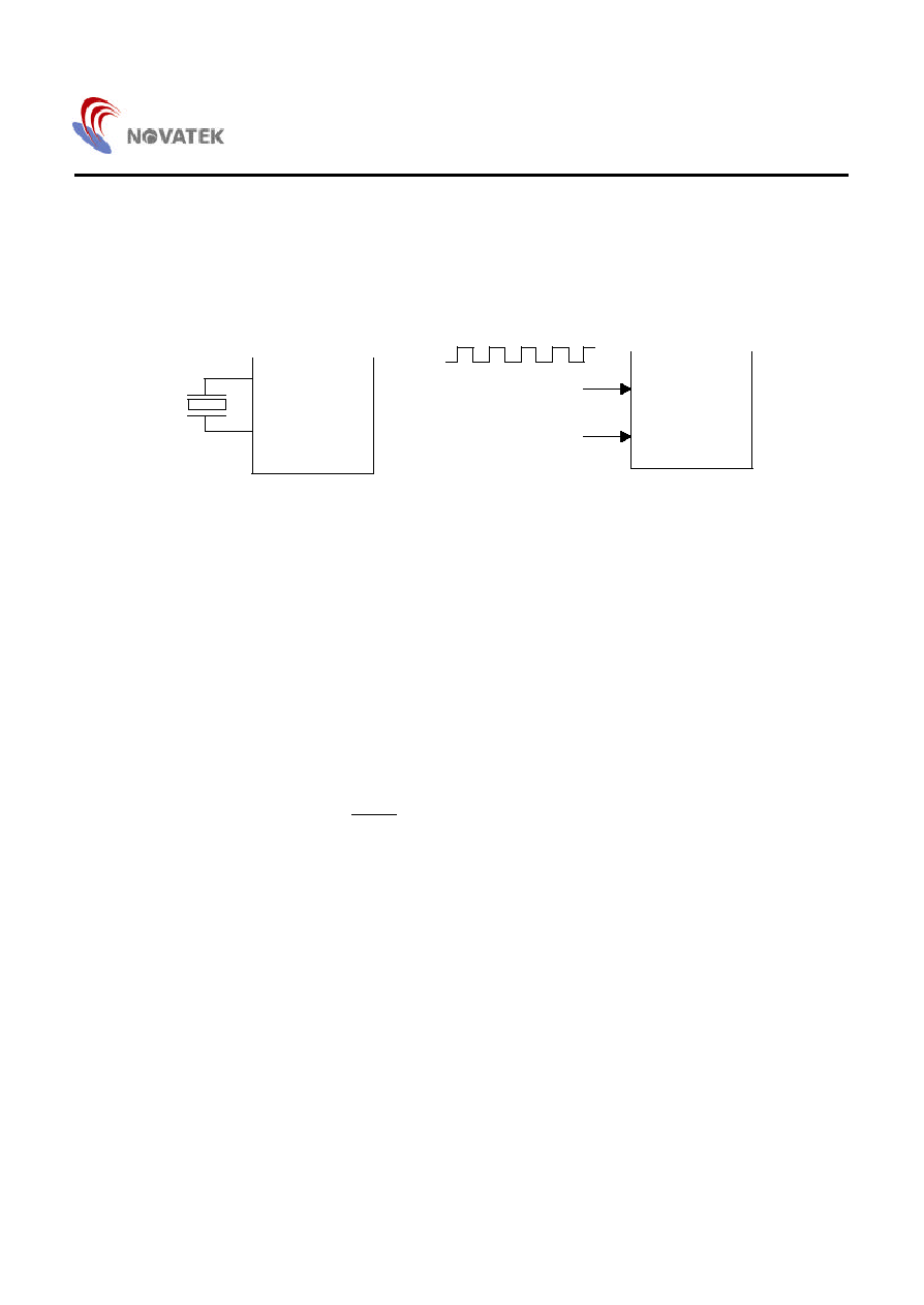
6. Timing Generator
This block generates the system timing and control signal
to be supplied to the CPU and on-chip peripherals. A
crystal quartz, ceramic resonator, or an external clock
signal which will be provided to the OSCI pin generates
system timing. It generates 8MHz system clock, 4MHz for
the CPU. Although internal circuits have a feedback resister
and compacitor included, users can externally add these
components for proper operating.
The typical clock frequency is 8MHz. Different frequencies
will affect the operation of those on-chip peripherals whose
operating frequency is based on the system clock.
8MHz
OSCI
OSCO
NT68P62
OSCI
NT68P62
Figure 6.1. Oscillator Connections
(1)
(2)
Unconnected
External Clock
OSCO
7. RESET
The NT68P62 can be reset by the external reset pin or by
the internal watch-dog timer. This is used to reset or start
the microcontroller from a POWER DOWN condition.
During the time that this reset pin is held LOW (*reset line
must be held LOW for at least two CPU clock cycles),
writing to or from the
�
C is inhibited. When a positive edge
is detected on the RESET input, the
�
C will immediately
begin the reset sequence.
After a system initialization time of six CPU clock cycles,
the mask interrupt flag will be set and the
�
C will load the
program counter from the memory vector locations $FFFC
and $FFFD. This is the start location for program control.
An internal Schmitt Trigger buffer at the RESET pin is
provided to improve noise immunity.
The reset status is as follows:
1. PORT0
PORT1
PORT2
PORT3 (& PORT4) pins
will act as I/O ports with HIGH output
2. Sync processor counters reset and VCNT | HCNT
latches cleared
3. All sync outputs are disabled
4. Base timer is disabled and cleared
5. Various Interrupt sources are disabled and cleared
6. A/D converter is disabled and stopped
7. DDC1/2B+ function is disabled
8. PWM DAC0 � DAC6 output 50% duty waveform and
DAC7 - DAC12 is disabled
9. Watch-dog timer is cleared and enabled

NT68P62-01
14
8. A/D Converters
The structure of these analog to digital converters is 6-bit
successive approximation. Analog voltage is supplied from
external sources to the A/D input pins and the result of the
conversion is stored in the 6-bit data latch registers ($0011
& $0014). The A/D channels are activated by clearing the
correspondent control bits in the ENADC control register.
When users write '0' into one of the enable control bits, its
correspondent I/O pin or DAC will be switched to the A/D
converter input pin (ADC0 & ADC1 shared with PORT10 &
PORT 11; ADC2 & ADC3 shared wit DAC0 & DAC1).
Conversion will be started by clearing CSTA bit
(CONVERSION START) in the ENADC control register.
When conversion is finished, system will set this INTADC
bit. Users can monitor this bit to get the valid A/D
conversion data in the AD latch registers ($0011 - $0014).
Users can also open interrupt sources to remind users to
get the stable digital data. Notice that only at the activated
A/D channel, its latched data are available.
The analog voltage to be measured should be stabled
during the conversion operation and the variation will not
exceed LSB for the best accuracy in measurement.
Addr.
Register
INIT
Bit7
Bit6
Bit5
Bit4
Bit3
Bit2
Bit1
Bit0
R/W
$0010
ENADC
FFH
CSTA
-
-
-
ENADC3
ENADC2
ENADC1
ENADC0
W
$0011
AD0 REG
C0H
-
-
AD05
AD04
AD03
AD02
AD01
AD00
R
$0012
AD1 REG
00H
-
-
AD15
AD14
AD13
AD12
AD11
AD10
R
$0013
AD2 REG
00H
-
-
AD25
AD24
AD23
AD22
AD21
AD20
R
$0014
AD3 REG
00H
-
-
AD35
AD34
AD33
AD32
AD31
AD30
R
$001B
IEIRQ2
00H
-
-
-
-
INTADC
INTV
INTE1
INTMR
R/W
$001E
IRQ2
00H
-
-
-
-
INTADC
INTV
INTE1
INTMR
R
-
-
-
-
CLRADC
CLRV
CLRE1
CLRMR
W
Reference ADC Table (V
DD
= 5.0V)
15
1.50V
1C
2.06V
23
2.59V
2A
3.14V
16
1.58V
1D
2.12V
24
2.67V
2B
3.22V
17
1.66V
1E
2.20V
25
2.75V
2C
3.30V
18
1.74V
1F
2.28V
26
2.82V
2D
3.38V
19
1.82V
20
2.35V
27
2.91V
2E
3.46V
1A
1.90V
21
2.44V
28
2.98V
2F
3.54V
1B
1.98V
22
2.51V
29
3.07V
30
3.62V
Note: It is strongly recommended that the ADC's input signal should be allocated in the ADC's linear voltage range
(1.5V~3.5V) to obtain a stable digital value. Do not use the outer ranges (0V~1.4V & 3.6V~5.0V) in which the
converted digital value is not guaranteed.

NT68P62-01
15
9. PWM DACs (Pulse Width Modulation D/A Converters)
There are 13 PWM D/A converters with 8-bit resolution in NT68P62. All of these D/A (DAC0 - DAC12) converters are open-
drain output structure with external 5V applied maximum. DAC0 � DAC6 are dedicated PWM channels, and DAC7 - DAC12
are shared with I/O pins. Those shared PWM channels are activated by clearing the correspondent control bits in the
ENDAC control register ($000F). When users write '0' into one of the enable control bits, its correspondent I/O pin will be
switched to PWM output pin.
The PWM refresh rate is 62.5KHz operating on 8MHz system clock. There are 13 readable DACH registers corresponding to
13 PWM channels ($0030 - $003D). Each PWM output pulse width is programmable by setting the 8 bit digital to the
corresponding DACH registers. When these DACH registers are set to 00H, the DAC will output LOW (GND level) and every
1 bit addition will add 62.5ns pulse width. After reset, all DAC outputs are set to 80H (1/2 duty output). (Please refer to Figure
9.1 for the detailed timing diagram of PWM D/A output.)
01
02
m
255(FF)
Fosc
255
0
1
2
m
255
1
PWM value :
8MHz
00
Figure 9.1. The DAC Output Timing Diagram and Wave Table
03
3
m-1
0

NT68P62-01
16
PWM DACs (continued)
DAC0 & DAC1 are shared with ADC2 & ADC3 input pins respectively. If ENADC2/
3
bit in the ENADC control register is
cleared to LOW, A/D converters will activate simultaneously. After the chip is reset, ENADC2/
3
bits will be in HIGH state
and DAC0 & DAC1 will act as PWM output pins.
DAC4 & DAC5 are shared with SCL1 & SDA1 I/O pins respectively. If users clear the
ENDDC
bit in the CH1CON control
register to LOW, channel 1 of DDC will be activated. When used as DDC channel, the I/O port will be an open drain structure
and include 'Schmitt Trigger' buffer for noise immunity. After the chip is reset,
ENDDC
bits will be in HIGH state and DAC4 -
DAC5 will act as PWM output pins.
Addr.
Register
INIT
Bit7
Bit6
Bit5
Bit4
Bit3
Bit2
Bit1
Bit0
R/W
$000F
ENDAC
FFH
-
-
ENDK12
ENDK11
ENDK10
ENDK9
ENDK8
ENDK7
W
$0010
ENADC
FFH
CSTA
-
-
-
ENADC3
ENADC2
ENADC1
ENADC0
W
$0030
DACH0
80H
DKVL7
DKVL6
DKVL5
DKVL4
DKVL3
DKVL2
DKVL1
DKVL0
RW
$0031
DACH1
80H
DKVL7
DKVL6
DKVL5
DKVL4
DKVL3
DKVL2
DKVL1
DKVL0
RW
$0032
DACH2
80H
DKVL7
DKVL6
DKVL5
DKVL4
DKVL3
DKVL2
DKVL1
DKVL0
RW
$0033
DACH3
80H
DKVL7
DKVL6
DKVL5
DKVL4
DKVL3
DKVL2
DKVL1
DKVL0
RW
$0034
DACH4
80H
DKVL7
DKVL6
DKVL5
DKVL4
DKVL3
DKVL2
DKVL1
DKVL0
RW
$0035
DACH5
80H
DKVL7
DKVL6
DKVL5
DKVL4
DKVL3
DKVL2
DKVL1
DKVL0
RW
$0036
DACH6
80H
DKVL7
DKVL6
DKVL5
DKVL4
DKVL3
DKVL2
DKVL1
DKVL0
RW
$0037
-
-
-
-
-
-
-
-
-
$0038
DACH7
80H
DKVL7
DKVL6
DKVL5
DKVL4
DKVL3
DKVL2
DKVL1
DKVL0
RW
$0039
DACH8
80H
DKVL7
DKVL6
DKVL5
DKVL4
DKVL3
DKVL2
DKVL1
DKVL0
RW
$003A
DACH9
80H
DKVL7
DKVL6
DKVL5
DKVL4
DKVL3
DKVL2
DKVL1
DKVL0
RW
$003B
DACH10
80H
DKVL7
DKVL6
DKVL5
DKVL4
DKVL3
DKVL2
DKVL1
DKVL0
RW
$003C
DACH11
80H
DKVL7
DKVL6
DKVL5
DKVL4
DKVL3
DKVL2
DKVL1
DKVL0
RW
$003D
DACH12
80H
DKVL7
DKVL6
DKVL5
DKVL4
DKVL3
DKVL2
DKVL1
DKVL0
RW
DAC control register ($000F) and DAC value register ($0030 - $003D)
NT68P62-01
17
10. Watch-Dog Timer (WDT)
The NT68P62 implements a watch-dog timer reset to avoid
system stop or malfunction. The clock of the WDT is from
on-chip RC oscillator which does not require any external
components. Thus, the WDT will run, even if the clock on
the OSCI/OSCO pins of the device have been stopped.
The WDT time interval is about 0.5 second. The WDT must
be cleared within every 0.5 second when the software is in
normal sequence, otherwise the WDT will overflow and
cause a reset. The WDT is cleared and enabled after the
system is reset, and can not be disabled by the software.
Users can clear the WDT by writing 55H to CLRWDT
register ($0020).
as;
LDA #$55
STA
$0020
Addr.
Register
INIT
Bit7
Bit6
Bit5
Bit4
Bit3
Bit2
Bit1
Bit0
R/W
$0020
CLR WDT
-
0
1
0
1
0
1
0
1
W
11. Interrupt Controller
The system provides two kinds of interrupt sources: NMI &
IRQ. The NMI can not be masked and if enabling NMI
interrupt sources, users will execute the NMI interrupt
vector anytime when sources are activated. The IRQ
interrupts can be masked by executing a CLI instruction or
setting the interrupt mask flag directly in the
�
C status
register. In process IRQ interrupt, if the interrupt mask flag
is not set, the
�
C will begin an interrupt sequence. The
program counter and processor status register will be
stored in the stack. The
�
C will then set the interrupt mask
flag HIGH so that no further interrupts may occur. At the
end of this cycle, the program counter will be loaded from
addresses $FFFE & $FFFF, then transferring program
control to the memory vector located at these addresses.
For NMI interrupt,
�
C will transfer execution sequence to
the memory vector located at addresses $FFFA & $FFFB.
When manipulating various interrupt sources, NT68P62
divides them into two groups for accessing them easily.
One is NMI group and the other is IRQ group.
- The NMI group includes INTE0, INTMUTE.
-
The IRQ group includes subgroup of IRQ0, IRQ1,RQ2:
IRQ0: DDC1/2B+ Channel 0 interrupt sources; It
includes INTS0, INTA0, INTTX0, INTRX0,
INTNAK0 and INTSTOP0 interrupts.
IRQ1: DDC1/2B+ Channel 1 interrupt sources; It
includes INTS0, INTA1, INTTX1, INTRX1,
INTNAK1 and INTSTOP1.
IRQ2: It includes INTADC, INTV, INTE1 and INTMR
interrupt sources.
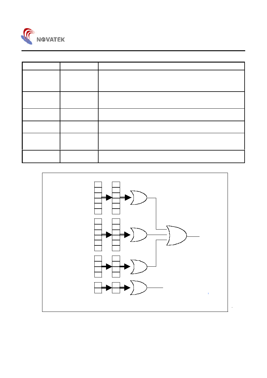
Below are the interrupt sources.
Nonmaskable Interrupt Group:
Interrupt
Meaning
Action
INTE0 INT
External 0 INT
It will be activated by the rising edge or falling edge of external interrupt pulse.
The triggered edge can be selected by EDGE0 bit.
INTMUTE
Auto Mute
It will be activated when the mute condition occurres (Hsync frequency
change). Please refer the synprocessor section for more detailed explanation.
Maskable Interrupt Group:
Interrupt
Meaning
Action
INTADC
A/D Converion
Done
User activates the ADC by clearing the
CSTART
bit. When AD conversion is
done, this bit will be set.
INTV INT
Vsync INT
It will be activated as the rising edge of every vsync pulse.
INTE1 INT
External 1 INT
It will be activated by the rising edge or falling edge of external interrupt pulse.
The triggered edge can be selected by EDGE1 bit.
INTMR INT
Timer INT
It will be activated as the rising edge of every when the Base Timer counter
overflows and counting from $FF to $00.
NT68P62-01
18
DDC Channel 0/1 Maskable Interrupt Sources:
Interrupt
Meaning
Action
INTS INT
SCL Go-Low INT
In DDC1 mode, it will be activated when the external device proceed a DDC2
communication. This action includes pull the SCL line to ground or send out an
'START' condition directly. System will respond to this action by changing
DDC1 mode to DDC2 slave mode.
INTA INT
Address Matched
INT
It will be activated at DDC2 slave mode when the external device call NT68P62
slave address. If this calling address matches the NT68P62 address, system
will generate this interrupt to remind user
INTTX INT
Transfer Buffer
Empty INT
It will be activated at DDC2 mode when transmission buffer, IIC_TXDAT, is
empty at transmission mode.
INTRX INT
Receiving Buffer
Overflow INT
It will be activated at DDC2 mode when new data have store in the
IIC_RXDAT register at receive mode.
INTNAK INT
No Acknowledge
INT
At transmission mode, this interrupt will be activated when NT68P62 have
send out one byte data but the external device does not respond an
acknowledge bit to it.
INTSTOP INT
DDC2 Stop INT
In SLAVE mode, this interrupt will be activated when the NT68P62 receives an
'STOP' condition.
INTSTOP0
INTNAK0
INTRX0
INTTX0
INTA0
INTS0
INTSTOP1
INTNAK1
INTRX1
INTTX1
INTA1
INTS1
INTMR
INTE1
INTV
INTADC
INTMUTE
INTE0
IRQ0
IRQ (to CPU 6502)
NMI (to CPU 6502)
IRQ0
IRQ1
IRQ2
Figure 11.1. Interrupt Controller Structure
IRQ1
IRQ2
IEIRQ0
IEIRQ1
IEIRQ2
NMIPOLL
IENMI

NT68P62-01
19
Enabling Interrupts: The system will disable all of these
interrupts after reset. Users can enable each of the
interrupts by setting the interrupt enable bits at IENMI,
IEIRQ0 - IEIRQ3 control registers. For example, if users
want to enable external interrupt 0 (INTE0), write '1' to
INTE0 bit in the IENMI control register. At the INTE0 pin,
whenever NT68P62 has detected an interrupt message, it
will generate an interrupt sequence to fetch the NMI vector.
Because these IEX control registers can be read, users can
read back what interrupts he has been activated. At polling
sequence, users need not poll those unactivated interrupts.
Requesting Interrupts to be set: No matter user have been
set the interrupt enable bits or not, if the interrupt triggered
condition is matched, system will set the correspondent bits
in the IRQ0 - IRQ3 control registers or in the NMIPOLL
control register (INTE0 & INTMUTE bits). For example, if at
VSYNCI pin, system have detected a pulse occurring,
system will set the INTV bit in the IRQ2 control register.
Interrupt Groups: System divides IRQ interrupt sources into
several groups, ex IRQ0, IRQ1, IRQ2 and IRQ3. At each of
these groups, if its membership in the one of the interrupt
groups have been activated, its group bit in the IRQPOLL
control register will be set. For example, if the INTS0 of the
first DDC1/2B+ channel is activated, the INTS0 bit in the
IRQ0 will be set and the IRQ0 bit in the IRQPOLL control
register also will be set. Notice that the IRQ0 bit will be
cleared by system when all of its membership of interrupt
sources, INTS0, INTTX0, INTRX0, INTNAK0 and
INTSTOP0 have been cleared by the user or system. The
NMI group is also oprating the same procedure as IRQ
groups.
Polling Interrupts: When NMI interrupt occurrs, at NMI
interrupt service routine, users must poll the INTE0 &
INTMUTE bit in the NMIPOLL control register to confirm the
NMI interrupt source. The polling sequence decides the
priority of NMI interrupt acceptation. When IRQ interrupt
occurrs, at IRQ interrupt service routine, users must poll the
IRQ0 - IRQ3 in the IRQPOLL control register to confirm the
IRQ interrupt source. In the same way, the polling
sequence decides the priority of IRQ interrupt acception.
When deciding the IRQ source, users can further confirm
the real interrupt source by polling the Correspondent IRQX
control register ($001C - $001E).
Clearing the Interrupt Request bit: When interrupt occurrs,
the CPU will jump to the address defined by the interrupt
vector to execute interrupt service routine. Users can check
which one of the interrupt sources is activated and
operating a tast. It is that upon entering the interrupt service
routine, the request bit that caused the interrupt must be
cleared by user before finishing the service routine and
returning to normal instruction sequence. If users forget to
clear this request bit, after returning to main program, it will
interrupt CPU again because the request bit remains
activated. Simply, users just need write '1' to the polling bits
in the NMIPOLL & IRQX registers ($0016 & $001C -
$001E) to clear those completed interrupt sources.
Selecting interrupt triggered edge: At INTV, INTE0 & INTE1
interrupt sources, these are now edge triggered type.
System provides the selection of rising or falling edge
triggered under user's control. After reset, the rising edge
triggered are provided and the content is 'FF' in the
TRIGGER control register ($001F). User just clear control
bits in this TRIGGER register and switch these interrupts to
falling edge triggered.
NT68P62-01
20
Control Bit Description
Addr.
Register
INIT
Bit7
Bit6
Bit5
Bit4
Bit3
Bit2
Bit1
Bit0
R/W
Control Register for Polling Interrupt
-
-
-
-
-
-
INTE0
INTMUTE
R
$0016
NMIPOLL
00H
-
-
-
-
-
-
CLRE0
CLRMUTE
W
$0017
IRQPOLL
00H
-
-
-
-
-
IRQ2
IRQ1
IRQ0
R
Control Registers of Interrupt Enable
$0018
IENMI
00H
-
-
-
-
-
-
INTE0
INTMUTE
RW
$0019
IEIRQ0
00H
-
-
INTS0
INTA0
INTTX0
INTRX0
INTNAK0
INTSTOP0
RW
$001A
IEIRQ1
00H
-
-
INTS1
INTA1
INTTX1
INTRX1
INTNAK1
INTSTOP1
RW
$001B
IEIRQ2
00H
-
-
-
-
INTADC
INTV
INTE1
INTMR
RW
Control Registers for Polling (Read) & Clearing (Write) Interrupt Requests
-
-
INTS0
INTA0
INTTX0
INTRX0
INTNAK0
INTSTOP0
R
$001C
IRQ0
00H
-
-
CLRS0
CLRA0
CLRTX0
CLRRX0
CLRNAK0 CLRSTOP0
W
-
-
INTS1
INTA1
INTTX1
INTRX1
INTNAK1
INTSTOP1
R
-
-
CLRS1
CLRA1
CLRTX1
CLRRX1
CLRNAK1 CLRSTOP1
W
$001D
IRQ1
00H
-
-
-
-
CLRADC
CLRV
CLRE1
CLRMR
W
Selection of Edge Triggered for INTE0 & 1 Interrupt
$001F
TRIGGER
FFH
-
-
-
-
-
INTVR
INTE1R
INTE0R
R/W

NT68P62-01
21
12. I/O PORTs
The NT68P62 has 25 pins dedicated to input and output.
These pins are grouped into 4 ports.
12.1. PORT0: P00 - P07
PORT0 is an 8-bit bi-directional CMOS I/O port with PMOS
as internal pull-up (Figure 12.1). Each pin of PORT0 may
be bit programmed as an input or output port without
software control the data direction register. When PORT0
works as output, the data to be output are latched to the
port data register and output to the pin. PORT0 pins that
have '1's written to them are pulled HIGH by the internal
PMOS pull-ups. In this state they can be used as input,
then the input signal can be read. This port output is HIGH
after reset.
P00 - P05 are shared with DAC7 - DAC12 respectively. If
ENDK7 - ENDK12
is set
to LOW in ENDAC register, P00 -
P05 will act as DAC7 - DAC12 respectively (Figure 12.2).
After the chip is reset, ENDK7 - ENDK12 will be in the
HIGH state and P00 - P05s will act as I/O ports.
P06
P07 are shared with VSYNCO & HSYNCO
respectively. If
ENHOUT
ENVOUT
is set
to LOW in
HVCON register, P06
P07 will act as VSYNCO &
HSYNCO respectively (Figure 12.3). After the chip is reset,
ENHOUT
&
ENVOUT
will be in the HIGH state and
P06
P07 will act as I/O pins.
Addr.
Register
INIT
Bit7
Bit6
Bit5
Bit4
Bit3
Bit2
Bit1
Bit0
R/W
$0000
PT0
FFH
P07
P06
P05
P04
P03
P02
P01
P00
RW
FFH
-
-
HSYNCI
VSYNCI
HPOLI
VPOLI
HPOLO
VPOLO
R
$0007
HV CON
FFH
ENHOUT
ENVOUT
-
-
-
-
HPOLO
VPOLO
W
$000F
ENDAC
FFH
-
-
ENDK12
ENDK11
ENDK10
ENDK9
ENDK8
ENDK7
W
V
DD
I/O
Data Out
Data In
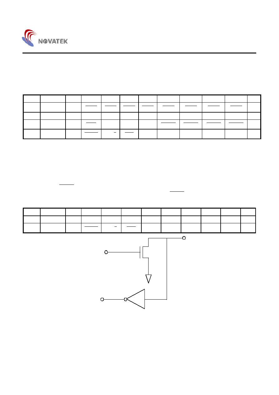
Figure 12.1. I/O Structure
PWM
Output
PWM
Data In
Figure 12.2. PWM Output Structure
V
DD
O/P
Data Out
Figure 12.3. Output Structure

NT68P62-01
22
12.2. Port1: P10 - P16
PORT10 - PORT16 is a 7-bit bi-directional CMOS I/O port
with PMOS as internal pull-up (Figure 12.1). Each bi-
directional I/O pin may be bit programmed as an input or
output port without software control the data direction
register. When PORT1 works as output, the data to be
output is latched to the port data register and output to the
pin. PORT1 pins that have '1's written to them are pulled
HIGH by the internal PMOS pull-ups. In this state they can
be used as input, then the input signal can be read. This
port output HIGH after reset.
P10 & P11 are shared with AD0 & AD1 input pins
respectively. If the ENADC0/1 bit in the ENADC control
register is cleared to LOW, A/D converters will activate
simultaneously. After the chip is reset, ENADC0/1 bits will
be in the HIGH state and P10 - P11 will act as I/O pins.
P12
P13 are shared with HALF SIGNALS input and
OUTPUT pins by accessing the OUTCON control register.
If the ENHALF bit is cleared to LOW, P13 will switch to
HALFHI pin (input pin) and P12 will switch to HALFHO pin
(output pin, Figure 12.3). For HALFHI & HALFHO pin
description, please refer half frequency function in the H/V
sync processor paragraph. After the chip is reset, the
ENHALF bits will be in HIGH state and P12
P13 will act
as I/O pins.
P14 is shared with output pin of self test pattern. If users
clear the PATTERN bit in the SYNCON control register
and the free running function has been activated, the P14
will switch to output pin of the self test pattern. This pattern
output pin is push-pull structure. After the chip is reset,
PATTERN bits will be in the HIGH state and P14 will act as
I/O pin. (Refer the 'Syncprocessor' section for more
detailed information.)
P15 & P16 can be shared with external interrupt INTE0 &
INTE1 pins if the INTE0/1 bits are set in the control register
of interrupt enable ($0016 & $0019). These interrupt pin
have 'Schmitt Trigger' input buffers. After the chip is reset,
INTE0/1 bits will be in HIGH state and P15 & P16 will act
as I/O pin.
Refer 'INTERRUPT CONTROLLER' paragraph above for
more details about the interrupt function.
Addr.
Register
INIT
Bit7
Bit6
Bit5
Bit4
Bit3
Bit2
Bit1
Bit0
R/W
$0001
PT1
7FH
-
P16
P15
P14
P13
P12
P11
P10
RW
$000C
FREECON
FFH
ENPAT
PAT0
-
-
-
FREQ2
FREQ1
FREQ0
W
$0010
ENADC
FFH
CSTA
-
-
-
ENADC3
ENADC2
ENADC1
ENADC0
W
$0018
IENMI
00H
-
-
-
-
-
-
INTE0
INTMUTE
RW
$001B
IEIRQ2
00H
-
-
-
-
-
INTV
INTE1
INTMR
RW
Data Input
I/P
V
DD
Figure 12.4. Schmitt Input Structure
V
DD
I/O
Data Out
.
Data OE
Data In
Figure 12.5. I/O Structure
NT68P62-01
23
12.3. PORT2: P20 - P27
PORT2, an 8-bit bi-directional I/O port (Figure 12.5), may be programmed as an input or output pin by the software control.
When setting the PT2DIR control bit to '0', its correspondent pin will act as an output pin. On the other hand, clear PT2DIR
bit to '1', act as input pin. When programmed as an input, it has an internal pull-up resistor. When programmed as an output,
the data to be output is latched to the port data register and output to the pin with push-pull structure. This port acts as input
port after reset.
Addr.
Register
INIT
Bit7
Bit6
Bit5
Bit4
Bit3
Bit2
Bit1
Bit0
R/W
$0002
PT2DIR
FFH
P27OE
P26OE
P25OE
P24OE
P23OE
P22OE
P21OE
P20OE
W
$0003
PT2
FFH
P27
P26
P25
P24
P23
P22
P21
P20
RW
$0010
ENADC
FFH
CSTA
-
-
-
ENADC3
ENADC2
ENADC1
ENADC0
W
$0029
CH1CON
FFH
ENDDC
MD1/
2
SRW
START
STOP
RXACK
TXACK
-
RW
12.4. PORT3: P30 - P31
PORT3 is an 2 bit bi-directional open-drain I/O port (Figure 12.6). Each pin of PORT3 may be bit programmed as an input or
output port with open drain structure. When PORT3 works as output, the data to be output is latched to the port data register
and output to the pin. When PORT3 pins that have '1's written to them, users must connect PORT3 with external pulled-up
resistor and then PORT3 can be used as input (the input signal can be read). This port output HIGH after reset.
P30
P31 include Schmitt Trigger buffers for noise immunity and can be configured as the I
2
C pins SDA0 & SCL0
respectively. If set ENDDC to LOW in CH0DDC control register, P30
P31 will act as SDA0 & SCL0 I/O pins respectively
and will be an open drain structure (Figure 12.6). After the chip is reset, this ENDDC bit will be in HIGH state and PORT3
will act as I/O pins.
Addr.
Register
INIT
Bit7
Bit6
Bit5
Bit4
Bit3
Bit2
Bit1
Bit0
R/W
$0004
PT3
FFH
-
-
-
-
-
-
P31
P30
RW
$0029
CH1CON
FFH
ENDDC
MD1/
2
SRW
START
STOP
RXACK
TXACK
-
RW
I/O
Data Out
Data In
Figure 12.6. PORT3
NT68P62-01
24
12.5. PORT4: P40 - P41
PORT4 is available only on the 42pin SDIP IC. PORT40 - PORT41 is an 2-bit bi-directional CMOS I/O port with PMOS as
internal pull-up (Figure 12.1). Each bi-directional I/O pin may be bit programmed as an input or output port without software
control the data direction register. When PORT4 works as output, the data to be output is latched to the port data register
and output to the pin. PORT4 pins that have '1's written to them are pulled HIGH by the internal PMOS pull-ups. In this state
they can be used as input. The input signal can be read. This port outputs HIGH after reset.
Addr.
Register
INIT
Bit7
Bit6
Bit5
Bit4
Bit3
Bit2
Bit1
Bit0
R/W
$0005
PT4
FFH
-
-
-
-
-
-
P41
P40
RW
13. H/V Sync Signals Processor
The functions of the sync processor include polarity detection, Hsync & Vsync signals counting, and programmable sync
signals output. It also provides 3-sets of free running signals and special output of test pattern at burn-in process when
activating the free running output function. The NT68P62 can properly handle either composite or separate sync signal
inputs even without sync signal input. As to processing the composite sync signal, a hardware separator will be activated to
extract the HSYNC signal under user controlled. The input at HSYNCI can be either a pure horizontal sync signal or a
composite sync signal. For the sync waveform refer to Figure 13.1 & Figure 13.2.
The sync processor block diagram is shown in Figure 13.3. Both VSYNCI & HSYNCI pins have Schmitt Trigger and filtering
process to improve noise immunity. Any pulse that is shorter than 125 ns, will be regarded as a glitch and will be ignored.
(a) Positive polarity
(b) Negative polarity
Figure 13.1. Separate H Sync. Waveform
(a) Positive Polarity
(b) Negative Polarity
Figure 13.2. Composite H Sync. Waveform

NT68P62-01
25
Enable
Enable
Enable
Enable
Reset
Reset
8us
16.384 ms
ENHSEL
Control
Logic
V sync.
Latch
H sync.
Latch
Sync
Separator
H
HPOLI
VPOLI
V
H
HPOLO
VPOLO
H & V
Sync.
Polarity
Detector
H Sync.
Output
Control
FREE_RUN
Control
VSYNC
INPUT
HSYNC
INPUT
HSYNCO
0
1
1
0
VSYNCO
HCNTL
HCNTH
Digital
Filter
VCNTL
VCNTH
S/C
V
0
1
V
Schmitt
Trigger
Digital
Filter
Schmitt
Trigger
H sync.
counter
V sync.
counter
V Sync.
Output
Control
S/C
INTV
V
0
1
HSEL
32.968 ms
AUTO
MUTE
INTMUTE
FREQ0/1/2
Pattern
O/P
Control
ENPAT, PAT10/1
PATTERN
Figure 13.3. Sync. Processor Block Diagram

NT68P62-01
26
13.1. V & H Counter Register: VCNTL/H, HCNTL/H
Vsync counter: VCNTL/H, the 14-bit READ ONLY register, contains information of the Vsync frequency. An internal counter
counts the numbers of 8us pulse between two VSYNC pulses. When a next VSYNC signal is recognized, the counter is
stopped and the VCNTH/L register latches the counter value and then the counter counts from zero again for evaluating next
VSYNC time interval. The counted data can be converted to the time duration between two successive Vsync pulses by time
8 us. If no VSYNC incoming, the counter will overflow and set VCNTOV bit (in VCNTH register) to HIGH. Once the VCNTOV
set to HIGH, it keeps in the HIGH state until writing '1' to it (CLRVOV bit).
Hsync counter: If the ENHSEL bit is set to HIGH, the internal counter counts the Hsync pulses between two Vsync pulses.
The HCNTL/H control registers contain the numbers of Hsync pulse between two Vsync pulses. These data can determine if
the Hsync frequency is valid or not to determine the accurate video mode.
The system supports two other options of interval for user counting the frequency of Hsync pulses. If users clear the
ENHSEL and set the HSEL bits properly, this internal counter counts the Hsync pulses during this system defined time
interval. The time interval is defined below:
ENHSEL
HSEL
Hsync Freq
Note
1
-
Disabled
After system reset or users disabling
0
0
16.384 ms
0
1
32.768 ms
After system reset, this interval will be disabled and the content of ENHSEL & HSEL0 bits are '1'. When this function is
disabled, the HCNTL/H counter is working on the VSYNC pulse. It is invalid to write '00' to them.
Latching the hsync counter: The counted value will be latched by the HCNTH/L register pairs which are updated by Vsync
pulse or system defined time interval. (Refer the Figure 13.4 for the opration of HCNTL/H counter.) If the counter overflows,
the HCNTOV bit (in HCNTH register) will be set to HIGH. Once the HCNTOV is set to HIGH, it keeps in the HIGH state until
writing '1' to it (CLRHOV bit). When setting this CLRHOV bit, the HCNT counter will not be reset to zero.
HSYNCI
VSYNCI
Latch HCNT register
Reset H sync. counter
Start pulse counting
Latch HCNT register
Reset H sync. counter
Start pulse counting
HSYNCI
16.384ms/32.768ms
(Setting HSEL0/1 bits)
Figure 13.4. Hsync Counter Operation

NT68P62-01
27
Composite H sync. waveform (H EOR V)
(1) HSYNCI
(2) HSYNCI
Composite H sync. waveform (H OR V)
2
�
s
Hsync pulse or no pulse, the output signal of Hsync will be inserted.
HSYNCO
Inserted Hsync Pulse
VSYNCO
Original
Hsync Pulse
Original
Hsync Pulse
Widen 9
�
s
Figure 13.5. Composite H & V Sync. Processing

NT68P62-01
28
VCNTOV = '1'
?
HCNTH = '00'
?
No
Yes
Yes
No
Read VCNT|HCNT
Counter Register
NORMAL Mode
Seperate Sync.
Freq.
Calculating
Set S/C = '0'
Clear VCNTOV & HCNTOV
Open INTV & clear INTV flag
VCNTOV = '1'
?
No
Yes
Yes
No
Return
STAND-BY Mode
Off Mode
Worng Mode
Yes
No
Suspend Mode
Return
Freq.
Calculating
1. Extract HCNTL/H
12 bit data
2. 12 bit data * Vsync. freq.
= Hsync. freq.
or 12 bits data/time interval
(16.382 or 32.968 ms)
3. Its reciprocal
is Hsync. time duration.
1. Extract VCNTL/H 14 bit data
2. 14 bits data * 8 us
= Vsync. time duration
3. Its reciprocal
is Vsync. freq.
Set S/C = '1' & ENSEL = ''0'
& SELECT TIME INTRVAL
(16.384 or 32.968ms)
Clear VCNTOV & HCNTOV
Delay 2 * TIME INTELVAL
NORMAL Mode
Composite Sync.
HCNTH ='00'
?
HCNTH = '00'
?
Sync. Mode
Processing
INTV ?
No
Yes
Delay 132 ms
Delay 132 ms
Read VCNT|HCNT
Counter Register
System Default:
Open INTV & clear INTV flag
S/C = '1' & ENSEL = '1'
Figure 13.6. H & V Sync. Software Control Flow Chart (for reference only)

NT68P62-01
29
13.2. Sync Processor Control Register:
Polarity: The detection of Hsync or Vsync polarity is
achieved by hardware circuit that samples the sync signal's
voltage level periodically. Users can read HPOLI & VPOLI
bit from HVCON register, which bit = '1' represents positive
polarity and '0' represents negative polarity. Furthermore,
users can read HSYNCI and VSYNCI bit in HVCON
register to detect H & V sync input signal. Users can control
the polarity of H & V sync output signal by writing the
appropriate data to the HPOLO and VPOLO bits in the
HVCON register, '1' represents positive polarity and '0',
negative polarity.
Composite sync: Users have to determine whether the
incoming signal is separate sync or composite sync and set
S/ C & ENHSEL / HSEL bit properly. If the input sync
signal is composite, after set S/ C to '0', the sync separator
block will be activated (please refer Figure 13.5). At the
area of Vsync pulse, there can exist Hsync pulses or not.
For the output of Hsync, users can active hardware to
interpolate the Hsync pulses in that area by clearing the
INSEN bit. The width of these inserted pulses is 2uS fixed
and the time interval is the same as previous one.
According to the last Hsync pulse outside the Vsync pulse
duration, the hardware will arrange the interval of these
hardware interpolated pulses. These inserted Hsync pulse
have 125 nS phase deviation maximum. The Vsync pulse
can be extracted by hardware from composite Hsync
signal, and the delay time of output Vsync signal will be
limited bellow 20ns. For inserting Hsync pulse safely, the
extracted Vsync pulse will be widens about 9
�
s. Because
evenly inserting the Hsync pulse, the last inserted Hsync
pulse will have different frequency from original ones.
System will not implement this insertion function, users
must clear INSEN bit in the SYNCON control register to
activate this function. After reset, S/ C & INSEN bits
default value is HIGH and clear the VCNT | HCNT counter
latches to zero.
Sync output: In pin assignment, VSYNCO & HSYNCO
represent Vsync & Hsync output which are shared with P06
& P07 respectively. If ENVOUT & ENHOUT is set to '0' in
HVCON register, P06 & P07 will act as VSYNCO &
HSYNCO output pins. When the input sync is separate
signal, the V/HSYNCO will output the same signal as input
without delay. But if the input sync is composite signal, the
VSYNCO signal will have fixed delay time about 20ns and
the HSYNCO has nonfixed delay time about 125ns.
Half frequency Input and output: In pin assignment, when
users set ENHALF bits to '0' in HALFCON register, the
HALFHO pin will act as output pin and output half of input
signal in the HALFHI pin with 50% duty (see Figure 13.7). If
set NOHALF to '0', HALFHO will output the same signal in
the HALFHI pin and user can control its polarity of output
HALFHO by setting HALFPOL bit, '1' for positive and '0' for
negative polarity. After the chip is reset, ENHALF
NOHALF & HALFPOL will be in the HIGH state and P12 &
P13 will act as I/O pins. It is recommended to add a Schmitt
Trigger buffer at front of the HALFI pin.
Free run signal output: User can select one of free running
frequency (list bellow) outputting to HYSNCO & VSYNCO
pin by setting the FREQ0/1/2 bits. If user does not enable
H/VSYNCO by clearing ENVOUT or ENHOUT bits, any
setting of FREQ0/1/2 bits will be invalid. After system
reset, NT68P62 does not provide free running frequency
and both of FREQ0/1/2 bits are set to ' 1'. The free running
frequency can be set according the table below:
Free Running Freq.
FREQ2
FREQ1
FREQ0
Hsync Freq.
Vsync Freq.
Note
1
0
0
0
8M/256=31.2K
Hsync/512=61.0Hz
Refer to
Figure 13.7
2
0
0
1
8M/4/9/5=44.4K
Hsync/512=86.8Hz
3
0
1
0
8M/128=62.5K
Hsync/3/5/7/8=74.4Hz
4
0
1
1
8M/4/5/5=80K
Hsync/1024=78.1Hz
5
1
0
0/1
8M/4/2/11=90.9K
Hsync/1024=88.7Hz
1
1
0
1
1
1
Disabled Free
Run function
After System
Reset
NT68P62-01
30
Self testing pattern: At activating free running function, the system will generate the testing pattern when clearing the
ENPAT bit. The PORT14 pin will switch from I/O pin to pattern output pin (push-pull structure). The system provides four
types of testing patterns. Refer the figure below. Set the PAT0 bits to select the pattern type (Figure 13.8). If the free run
function has not been enabled, any change of ENPAT & PAT0 bits will be invalid. Refer the Figure 13.9 for the porch time
of video pattern.
PAT0
Test Pattern
Note
0
(1)
Only activated on ENPAT bit be cleared
1
(2)
The porch of self test pattern are listed below:
Free Running
Freq.
Front Porch of
VBLANK
BACK Porch of
VBLANK
Front Porch of
HBLANK
BACK Porch of
HBLANK
VSYNC
PULSE WIDTH
HSYNC
PULSE WIDTH
1
128
�
s
864
�
s
460ns
2.00
�
s
64
�
s
1
�
s
2
90.5
�
s
589
�
s
1.18
�
s
1.93
�
s
64
�
s
1
�
s
3
51
�
s
528
�
s
424ns
1.92
�
s
64
�
s
1
�
s
4
51.5
�
s
596
�
s
185ns
1.94
�
s
64
�
s
1
�
s
5
46.6
�
s
515
�
s
436ns
1.94
�
s
64
�
s
1
�
s
Mode change detection: The system provides a hardware detection of Sync signal changed and support user to respond to
this transition an proper process as soon as possible. There are three kinds of detections to set INTMUTE bit.
Hsync counter: Users can enable HDIFF comparison by clearing ENHDIFF bit and then preload an difference value to
HDIFF0-3 bits in the AUTOMUTE control register ($000E). The system will latch the new value of Hsync counter and
compare it with the last latched value. If this difference is great than this user defined value at HDIFF0-3 bits, system will set
the INTMUTE interrupt bit.
H/V polarity: Users can enable polarity detection by clearing ENPOL bit. The system will set the INTMUTE bit when the
polarity of Hsync or Vsync have been changed.
H/V counter overflow: Users can enable the detection of sync counters overflow by clearing ENOVER bit. The system will
set the INTMUTE bit whenever the counter of Hsync or Vsync has been overflowed.
The above three sources of setting this INTMUTE bit can be enabled or disabled by user. If user opens this interrupt, the
system will generate an NMI interrupt to remind users anytime. At user's manipulation, a software debounce to confirm the
transition of sync signal for one more times will make this system stable and reliable, but it will affect the response time. After
system reset, this 'automute' function will be disabled and the HDIFF0-2 control bits will be cleared to ' $0F'.
HALFHI
HALFHO: Half freq. Output signal (50% duty)
HALFHO output signal when NOHALF bit clear to LOW
(the same signal as in the HALFHI pin)
Figure 13.7. Half Freq. Sync. Waveform

NT68P62-01
31
(1)
(2)
Figure 13.8. Two Types of Testing Pattern
Back-Porch
Back-Porch
Front-Porch
Front-Porch
64
�
s
VSYNC
HSYNC
1
�
s
Video
Video
Figure 13.9. The Porch of Free Running Self Test Pattern

NT68P62-01
32
13.3 Power Saving Mode detect:
Video mode is listed as below, especially from mode 2 to mode 4 just for power saving. All of modes can be detected by
NT68P62 (Figure 13.6). These modes can be easily be detected.
Mode
H-Sync
V-Sync
(1) Normal
Active
Active
(2) Stand-by
Inactive
Active
(3) Suspend
Active
Inactive
(4) Off
Inactive
Inactive
Control Bit Description:
Addr.
Register
INIT
Bit7
Bit6
Bit5
Bit4
Bit3
Bit2
Bit1
Bit0
R/W
Control Registers for Synprocessor
FFH
-
-
-
-
INSEN
-
HSEL
S/
C
R
$0006
SYNCON
FFH
-
-
-
-
INSEN
ENHSEL
HSEL
S/
C
W
FFH
-
-
HSYNCI VSYNCI
HPOLI
VPOLI
HPOLO
VPOLO
R
$0007
HV CON
FFH
ENHOUT
ENVOUT
-
-
-
-
HPOLO
VPOLO
W
$0008
HCNT L
00H
HCL7
HCL6
HCL5
HCL4
HCL3
HCL2
HCL1
HCL0
R
HCNTOV
-
-
-
HCH3
HCH2
HCH1
HCH0
R
$0009
HCNT H
00H
CLRHOV
-
-
-
-
-
-
-
W
$000A
VCNT L
00H
VCL7
VCL6
VCL5
VCL4
VCL3
VCL2
VCL1
VCL0
R
VCNTOV
-
VCH5
VCH4
VCH3
VCH2
VCH1
VCH0
R
$000B
VCNT H
00H
CLRVOV
-
-
-
-
-
-
-
W
$000C
FREECON
FFH
ENPAT
PAT0
-
-
-
FREQ2
FREQ1
FREQ0
W
$000D
HALFCON
FFH
ENHALF
NOHALF
HALFPOL
-
-
-
-
-
W
$000E
AUTOMUTE
FFH
ENHDIFF
ENPOL
ENOVER
-
HDIFFVL3 HDIFFVL2 HDIFFVL1 HDIFFVL0
W
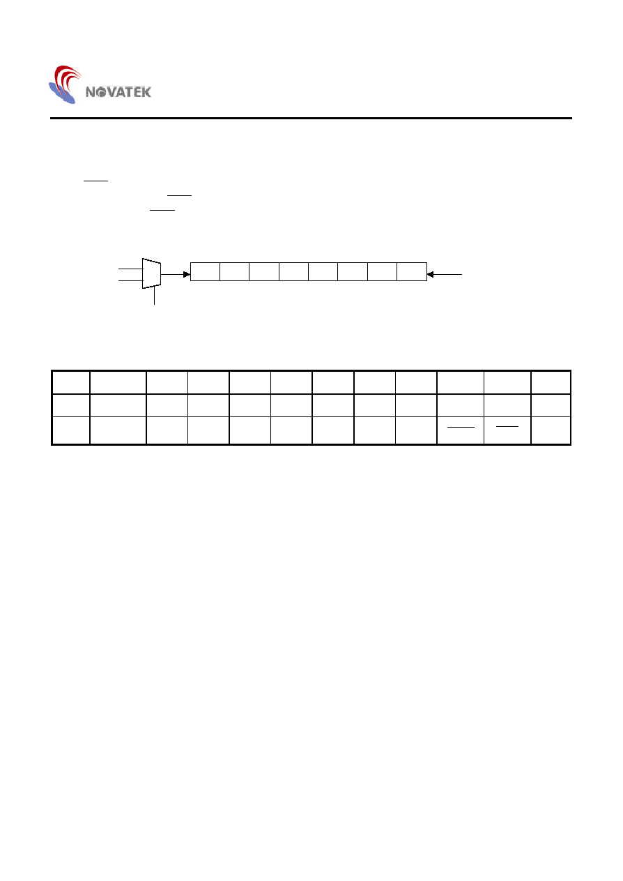
NT68P62-01
33
14. Base Timer (BT)
The BASE TIMER is an 8-bit counter, and its clock source
can be chosen with 1
�
s or 1ms by setting the BTCLK bit ('0'
for 1
�
s and '1' for 1ms). The BT can be enabled or disabled
by the ENBT bit in the BTCON register. The BT will start
counting while clearing the ENBT bit to `0'. After the chip is
reset, the BTCLK and ENBT bits are set to '1' (the BT is
disabled). Before enabling the BT, it can be preloaded with
a value by writing a value to the BT register (write only) at
any time and then the BT will start to count up from this
preloaded value. When the BT's value reaches FFH, it will
generate a timer interrupt if the timer interrupt is enabled,
and then the counter will wrap around to 00H. The timer's
maxium interval is 256ms or 256
�
s depending on the
BTCLK value.
BT7
INTMR INT
1us
1ms
BTCLK
1
0
BT6
BT5
BT4
BT3
BT2
BT1
BT0
Control Bit Description:
Addr.
Register
INIT
Bit7
Bit6
Bit5
Bit4
Bit3
Bit2
Bit1
Bit0
R/W
$002E
BT
00H
BT7
BT6
BT5
BT4
BT3
BT2
BT1
BT0
W
$002F
BT CON
03H
-
-
-
-
-
-
BTCLK
ENBT
W

NT68P62-01
34
15. I
2
C Bus Interface: DDC1 & DDC2B Slave Mode
Interface: I
2
C bus interface is a two-wire, bi-directional
serial bus which provides a simple, efficient way for data
communication between devices, and minimizes the cost of
connecting among various peripheral devices. NT68P62
provides two I
2
C channels. Both of them are shared with
I/O pins and their structures are open drain. When the
system is reset, these channels are originally general I/O
pins structure. All of these I
2
C bus function will be activated
only after their ENDDC bits are cleared to '0' (CH0/1CON
registers).
DDC1 & DDC2B+ function: Two modes of operation have
been implemented in NT68P62, uni-directional mode
(DDC1 mode) and bi-directional mode (DDC2B+ mode).
These channels will be activated as DDC1 function initially
when users enable DDC function. These channels will
switch automatically to DDC2B+ function from DDC1
function when a low pulse greater than 500ns is detected
on the SCL line. Users can start a master communication
directly from DDC1 communication by clearing MODE bit
in the CH0/1CLK control register.
The channels can return to DDC1 function when users set
the MD1/ 2 bit to '1' in the CH0/1CON registers.
15.1. DDC1 bus interface
Vsync input and SDA pin: In DDC1 function, the Vsync pin
is used as input clock pin and SDA pin is used as data
output pin. This function comprises two data buffers: one is
preloading data buffer for putting one byte data in advance
by user (CH0/1TXDAT), and the other is shift register for
shifting out one bit data to SDA line, which users can not
access directly. These two data buffer cooperate properly.
For the timing diagram please refer to Figure 15.1. After
system resets, the I
2
C bus interface is in DDC1 mode.
Data transfer: At first, user must put one byte transmitted
data into CH0/1TXDAT register in advance, and activate
I
2
C bus by setting ENDDC bit to '0'. Then open INTTX0/1
interrupt source by setting INTTX0/1 to '1' in the IEIRQ0/1
registers. On the first 9 rising edges of Vsync, system will
shift out invalid bit in shift register to SDA pin to empty shift
register. When shift register is empty and on next rising
edge of Vsync, it will load data in the CH0/1TXDAT
registers to internal shift register. At the same time,
NT68P62 will shift out MSB bit and generate an INTTX0/1
interrupts to remind user to put next byte data into
CH0/1TXDAT register. After eight rising clocks, there have
been eight bits shifted out in proper order and shift register
becomes empty again. At the ninth rising clock, it will shift
the ninth bit (null bit '1') out to SDA. And on the next rising
edge of Vsync clock, system will generate an INTTX0/1
interrupts again. By the same way, NT68P62 will load new
data from CH0/1TXDAT registers to internal shift register
and shift out one bit right away. Beware that user should
put one new data into CH0/1TXDAT registers properly
before the shift register is empty (the next INTTX0/1
interrupt). If not, the hardware will tansmit the last byte data
repeatedly.
Vsync clock: Only in the separate SYNC mode, can the
Vsync pulse be used as data transfer clock, its frequency
can be up to 25KHz maximum. In composite Vsync mode,
NT68P62 can not transmit any data to SDA pin, regardless
whether the Vsync can be extracted from composite Hsync
signal.
NT68P62-01
35
Control Bit Description:
Addr.
Register
INIT
Bit7
Bit6
Bit5
Bit4
Bit3
Bit2
Bit1
Bit0
R/W
-
-
-
-
-
-
INTE0
INTMUTE
R
$0016
NMIPOLL
00H
-
-
-
-
-
-
CLRE0
CLRMUTE
W
$0017
IRQPOLL
00H
-
-
-
-
-
IRQ2
IRQ1
IRQ0
R
$0019
IEIRQ0
00H
-
-
INTS0
INTA0
INTTX0
INTRX0
INTNAK0
INTSTOP0
RW
$001A
IEIRQ1
00H
-
-
INTS1
INTA1
INTTX1
INTRX1
INTNAK1
INTSTOP1
RW
-
-
INTS0
INTA0
INTTX0
INTRX0
INTNAK0
INTSTOP0
R
$001C
IRQ0
00H
-
-
CLRS0
CLRA0 CLRTX0
CLRRX0
CLRNAK0 CLRSTOP0
W
-
-
INTS1
INTA1 INTTX1
INTRX1
INTNAK1
INTSTOP1
R
$001D
IRQ1
00H
-
-
CLRS1
CLRA1 CLRTX1
CLRRX1
CLRNAK1 CLRSTOP1
W
Control Register for DDC1/2B+ of Channel 0
$0021
CH0ADDR
A0H
ADR7
ADR6
ADR5
ADR4
ADR3
ADR2
ADR1
-
W
$0022
CH0TXDAT
00H
TX7
TX6
TX5
TX4
TX3
TX2
TX1
TX0
W
$0023
CH0RXDAT
00H
RX7
RX6
RX5
RX4
RX3
RX2
RX1
RX0
R
MD1/
-
START
STOP
-
TXACK
-
W
$0024
CH0CON
E0H
-
-
START
STOP
RXACK
-
-
R
$0025
CH0CLK
FFH
-
-
DDC2BR2 DDC2BR1
DDC2BR0
W
Control Register for DDC1/2B+ of Channel 1
$0026
CH1ADDR
A0H
ADR7
ADR6
ADR5
ADR4
ADR3
ADR2
ADR1
-
W
$0027
CH1TXDAT
00H
TX7
TX6
TX5
TX4
TX3
TX2
TX1
TX0
W
$0028
CH1RXDAT
00H
RX7
RX6
RX5
RX4
RX3
RX2
RX1
RX0
R
MD1/
-
START
STOP
-
TXACK
-
W
$0029
CH1CON
E0H
-
-
START
STOP
RXACK
-
-
R
$002A
CH1CLK
FFH
-
-
DDC2BR2 DDC2BR1
DDC2BR0
W

NT68P62-01
36
(in CH0CON register)
Second Byte Data
First Byte Data
User can load next byte data
to CH0TXDAT register
Load data in the CH0TXDAT
register to shift register
Figure 15.1. DDC1 Mode Timing Diagram
15.2. DDC2B + Slave & Master Mode Bus Interface
The built-in DDC2B+ I
2
C bus Interface features as follows
-
SLAVE mode (NT68P62 is addressed by a master
which drives SCL signal)
-
MASTER mode (NT68P62 addresses external device
and send out SCL clock)
-
Compatible with I
2
C bus standard
-
One default address (A0H) and one programable
address
-
Automatic wait state insertion
-
Interrupt generation for status control
-
Detection of START and STOP signals
The DDC2B+ will be activated as SLAVE mode initially.
Users can switch to MASTER mode by clearing the
bit under either of these conditions listed as follows:
1. After entering to DDC1 function and clearing this bit, the
system will be changed from DDC1 to DDC2B+
MASTER mode operation.
2. After entering to DDC2B+ slave mode function and
clearing this bit, the system will changed from slave
mode into master mode operation.
As clearing
bit, system will send out a 'START'
condition and wait for user to put the calling address into
CH0/1TXDAT control register. Notice that user must
predetermine the direction of master mode transmission
before putting calling address.
Below is the DDC2B+ function with channel 0, and the
manipulation of channel 1 is the same as channel 0.

NT68P62-01
37
CONDITION
CONDITION
Figure 15.2. DDC2B Data Transfer

NT68P62-01
38
(external device)
(b) WRITE Mode Timing Diagram
(a) WRITE Mode Data Format
Data transferred
from external device
From external device to NT68P62
From NT68P62 to external device
A = Acknowledge
Figure 15.3. DDC2B Write Mode Spec.

NT68P62-01
39
(external device)
(b) READ Mode Timing Diagram
(a) Read Mode Data Format
From external device to NT6862
From NT6862 to external device
A = Acknowledge
A = No acknowledge
Data transferred
from NT6862
NT68P62 Address
user load first data into TXDAT buffer
Figure 15.4. DDC2B Read Mode Spec.
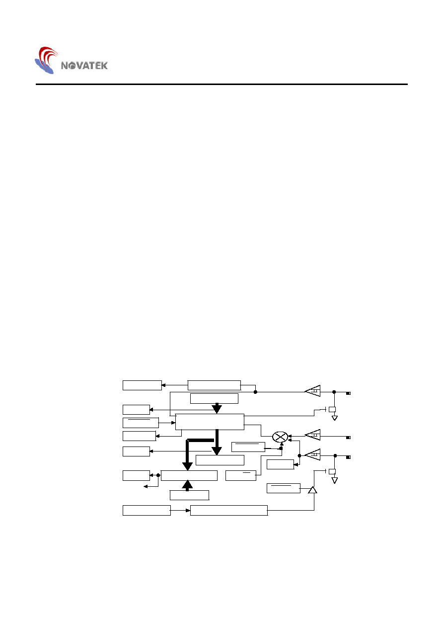
NT68P62-01
40
15.3. DDC2B Slave Mode Bus Interface
Enable I
2
C and INTS: After user clears the
to `0',
NT68P62 will enter into DDC1 mode, and it will switch to
DDC2B SLAVE mode while a low pulse is detected on SCL
line. The DDC2B bus consists of two wires, SCL and SDA;
SCL is the data transmission clock and SDA is the data
line. NT68P62 will remind user that the mode has changed
by generating a INTS interrupt. When users set MD1/ to
'1' at this time, the NT68P62 will return back to DDC1
mode. (For DDC2B please refer to Figure 15.2.) The figure
exhibits what are important in I
2
C: START signal, slave
ADDRESS, transferred data (proceed byte by byte) and a
STOP signal.
Start condition: When SCL & SDA lines are at HIGH state,
an external device (master) may initiate communication by
sending a START signal (defined as SDA from high to low
transition while SCL is at high state). When there is a
START condition, NT68P62 will set the 'START' bit to '1'
and user can poll this status bit to control DDC2B
transmission at any time. This bit will keep '1' until user
clears it. After sending a START signal for DDC2B
communication, an external device can repeatedly send
start condition without sending a STOP signal to terminate
this communication. This is used by external device to
communicate with another slave or with the same slave in
different mode (Read or Write mode) without releasing the
bus.
Address matched and INTA0: After the START condition, a
slave address is sent by an external device. When I
2
C bus
interface changes to DDC2B mode, NT68P62 will act as a
receiver first to receive this one byte data. This address
data is 7 bits long followed by the eighth bit (R/W) that
indicates data transfer direction. When the NT68P62
system receives an address data from an external device, it
will store it in the CH0RXDAT register. The system
supports 'A0' default address and another one set of
addresses which can be accessed by writting the
CH0ADDR register. Upon receiving the calling address
from an external device, the system will compare this
received data with the default 'A0' address and data in the
CH0ADDR register. Either of these address matched, the
system will set the INTA0 bit in the IRQ0 register. If the
user sets INTA0 bit to '1' (in IEIRQ0 register) in advanced
and addresses match, the NT68P62 will generate a INTA0
interrupt. Under the address matching condition, the
NT68P62 will send an acknowledge bit to an external
device. If address does not match, the NT68P62 will not
generate INTA0 interrupt and neglect the data change on
SDA line in the future.
Data transmission direction: In INTA0 interrupt servicing
routine, user must check the LSB of address data in
CH0RXDAT register. According to I
2
C bus protocol, this bit
indicates the DDC2B data transfer direction in later
transmission; '1' indicates a request for 'READ MODE'
action (external master device read data from system), '0'
indicates a 'WRITE MODE' action (external master device
write data to system). The timing about READ mode and
WRITE mode please refer to Figure 15.3 and Figure 15.4.
The data transfer can proceeded byte by byte in a direction
specified by the R/
bit after a successful slave address
is received.
The system will switch to either 'READ' mode or 'WRITE'
mode automatically
which is determined by this direction
bit.
Figure 15.5. DDC Structure Block
TXDAT
TXACK
9 bits Shift Register
Compare Logic
ADDR
RXDAT
INTA
ENDDC
in
out
clk
INTTX
INTRX
INTNAK
DDC2BR [2..0]
Clock Generator
SDA
VSYNC
SCL
INTS
MODE
MD1/2
R/W
STOP Detector
INTSTOP

NT68P62-01
41
Data transfer and wait: The data on the SDA line must be
stable during the HIGH period of the clock on the SCL line.
The HIGH and LOW state of the SDA line can only change
when the clock signal on the SCL line is LOW. Each byte
data is eight bits long and one clock pulse for one bit of
data transfer. Data is transferred with the most significant
bit (MSB) first. In the wired-AND connection, any slower
device can hold the SCL line LOW to force the faster
device into a wait state. Data transmition will be suspended
until the slower device is ready for the next byte transfer by
releasing the SCL line.
Acknowledge: The acknowledgment will be generated at
ninth clock by whom receiving data. In the WRITE MODE,
NT68P62 system must respond to this acknowledgment.
Users should clear the
bit in the CH0CON to open
the `ACK' function. After receiving one byte data from
external device, NT68P62 will automatically send this
acknowledgment bit.
In the READ mode, an external device must respond to the
acknowledgment bit after every byte data is sent out. The
system will set the INTNAK bit when external device does
not send out the '0' acknowledgment bit. Furthermore, user
can open this interrupt source by clearing the INTNAK bit in
the IEIRQ0 register.
The INTTX0 & INTRX0 interrupt: After NT68P62 complete
one byte transmission or receiving, it will generate an
INTTX0 (READ mode) & INTRX0 (WRITE mode) interrupts.
These interrupts are generated at the falling edge of the
ninth clock. Users can control the flow of DDC2B
transmission at these interrupts.
The INTRX0 on the WRITE mode: NT68P62 read data
from external master device. When users detect an
INTRX0 interrupt, it means there has one byte data
received and user can read out by accessing CH0RXDAT
control register. At the same time, if user responded an
'ACK' signal beforehand, the shift register will send out this
'ACK' bit (low voltage) and continue to receive the next byte
data. If both of shift register and CH0RXDAT register are
full and user still did not load data from CH0RXDAT
register, the SCL will be held LOW and waiting for
NT68P62. After user obtains one byte data from
CH0RXDAT register, the SCL will be released for
generation of SCL transmission clock. External device can
continue sending next byte data to NT68P62. The timing
diagram refers to Figure 15.3. User must responde a NAK
signal in advance to stop the transmission.
The INTTX0 on the READ mode: External device read data
from NT68P62. At INTTX0 interrupt, the system will load
new data from CH0TXDAT register which has been put by
user beforehand into internal shift register and continue
sending out this new data. After this new loading data be
shifted out according every SCL clock, system will request
user to put next byte data into CH0TXDAT register.
If both of shift register and CH0TXDAT register are empty
and user still not load data to CH0TXDAT register, the SCL
will be held LOW and waiting by NT68P62 after receiving
the acknowledgment bit.
At SCL holded low by system, after user has put one new
byte data into CH0TXDAT register, the SCL will be
released for generation of SCL transmission clock. At this
time, system will load this byte data into shift register and
generate a INTTX0 interrupt again to remind user putting
next byte into CH0TXDAT register. The timing diagram
refer to Figure 15.4.
After every one byte data transfer, system will monitor if
external master device has sent out this acknowledgment
bit or not. If not, system will set the INTNAK bit (the
acknowledgment is LOW signal). Users will get a INTNAK
interrupt if INTNAK has been enabled as a interrupt source.
STOP condition: When SCL & SDA line have been
released (hold on 'high' state), DDC2B data transfer is
always terminated by a STOP condition generated by
external device. A STOP signal is defined as a LOW to
HIGH transition of SDA while SCL is at HIGH state. When
there is a STOP condition, NT68P62 will set the 'STOP' bit
& INTSTOP bit to '1' and user can poll this status bit or
open a INTSTOP interrupt to control DDC2B transmission
at any time. This bit will keep '1' until user clears it by
writing '1' to this bit. Notice the SCL and SDA lines must
conform to I
2
C bus specifications. For the software
flowchart can please refer Figure 15.6. Please refer to the
standard I
2
C bus specification for details.
Change to DDC1 mode: After an external device terminates
DDC2 transmission by sending a STOP condition, users
can set MD1/ to '1' for changing to DDC1 mode. On the
other hand, when the SCL line has been released (pulled-
up), user can force NT68P62 to DDC1 mode
communication at any time.

NT68P62-01
42
IRQ0/1 Group
Service Routine
Change To DDC2
Slave Mode &
RECEIVING Mode
Put Slave Addr. Into
INTRX, INTNAK
Put One Byte data Into
CH0TXDAT Reg.
Read Out the SRW bit
Reset Buffer Index
INTTX & INTS
Put One Byte
CH0TXDATReg.
DDC1 Mode
(MD_CON = 1)
Read One Byte
CH0RXDAT Reg.
Put $FF Into
CH0TXDAT Reg.
(release SDA line)
INTTX, INTNAK &
INTA & INTV
INTRX, INTNAK &
INTTX, INTNAK
System release SCL &
SDA & send out STOP
condition User can do
some process
Transmission failed
SLAVE Mode Operation
Figure 15.6. Slave Mode INT Operation

NT68P62-01
43
15.4 DDC2B+ Master Mode Bus Interface
Most of the DDC manipulation is the same as SLAVE mode
except the SCL clock generation. In the MASTER mode,
the control of SCL clock source belongs to NT68P62. Users
must set the calling address and transmission direction in
advance. Access the
&
bits to control the
transmission flow of DDC2B+ master mode
communication.
Start condition: After user clearing
&
bit,
the system will generate a 'START' condition on the SCL &
SDA lines and wait for user to put the calling address into
TXDAT buffer and send to SDA line. The frequency of SCL
is dependant on the baud-rate setting value (DDCBR0 -
DDCBR2) in register CH0CLK. And the data transmission
direction will be dependant on the
bit and the LSB of
calling address, '1' for read operation and '0' for write
operation.
Calling address: Calling address is 8 bits long. It should be
put in the CH0TXDAT. The setting of LSB bit in this TXDAT
buffer should be as same as
bit.
STOP condition: There are several cases that the system
will send out 'STOP' condition on the SCL & SDA lines.
First, in the 'READ' operation, if user sets TXACK bit to '1',
the system will send out 'NAK' condition on the bus after
receiving one byte data and then send out 'STOP' condition
automatically later. Second, in the 'START' condition and
after sending out calling address, if no slave has respond to
a 'ACK' signal, the master will send out 'STOP' condition
automatically. Third, if user sets
bit to '1', the
system will generate a 'STOP' condition after the current
byte transmission is done. Notice that if slave device did
not released SCL and SDA line, the system can not send
out 'STOP' condition.
After 'STOP' condition, the master will release SCL & SDA
lines and return to SLAVE mode.
The INTTX0 & INTRX0 interrupt: After NT68P62
completing one byte transmission or receiving, it will
generate an INTTX0 (WRITE mode) & INTRX0 (READ
mode) interrupts. Users can control the flow of DDC2B
transmission at these interrupts.
The INTRX0 on the read mode: NT68P62 reads data from
external slave device. When users detect a INTRX0
interrupt, it means there is one byte data received and user
can read out by accessing CH0RXDAT control register. At
the same time, if the user responded an 'ACK' signal
beforehand, the shift register will send out an 'ACK' bit (low
voltage) and continue to receive next byte data. If both the
shift register and CH0RXDAT register are full and user still
did not load data from CH0RXDAT register, the SCL will be
held LOW and wait for NT68P62. After user has received
one byte data from CH0RXDAT register, the SCL will be
released for generation of SCL transmission clock. An
external device can continue sending next byte data to
NT68P62. Refer Figure 15.7 for the timing diagram. User
must respond to a NAK signal in advance to stop the
transmission. Before the last two bytes of data is received,
user should respond an 'NAK' signal. Then, system will
send out 'NAK' bit after receiving the last byte data and
'STOP' condition to notify the slave terminated current
transmission.
The INTTX0 on the WRITE mode: External device read
data from NT68P62. At INTTX0 interrupt, the system will
load new data from CH0TXDAT register which has been
put by user beforehand into internal shift register and
continue sending out this new data. After this new loading
data be shifted out according every SCL clock, system will
request user to put next byte data into CH0TXDAT register.
If both of shift register and CH0TXDAT register are empty
and user still not load data to CH0TXDAT register, the SCL
will be held LOW and wait for NT68P62 after receiving the
acknowledgment bit.
If SCL is held low by system, and user has put one new
byte data into CH0TXDAT register, the SCL will be
released for generation of SCL transmission clock. At this
time, system will load this byte data into shift register and
generate an INTTX0 interrupt again to remind user putting
next byte into CH0TXDAT register. Refer to Figure 15.8 for
the timing diagram.
Repeat start condition: If clearing the
bit to '0' in
the ' WRITE' operation, system will send out a 'REPEAT
START'. Notice that if slave device did not release SCL and
SDA line, the system can not send out 'REPEAT START
condition.
SCL baud rate selection: There are three Baud Rate bits for
user to select one of eight clock rates on the SCL line. After
system reset, the default value of these Baud Rate bits
(DDC2BR0-2) are '111'.

NT68P62-01
44
DDC2BR2
DDC2BR1
DDC2BR0
Baud Rate
0.00
0.00
0.00
400K
0.00
0.00
1.00
200K
0.00
1.00
0.00
100K
0.00
1.00
1.00
50K
1.00
0.00
0.00
25K
1.00
0.00
1.00
12.5K
1.00
1.00
0.00
6.25K
1.00
1.00
1.00
3.125K
(external device
putting data)
Figure 15.7. DDC2B+ MASTER READ Mode Timiing
1 2 3 4 5 6 7 8
If user read out first byte data from RXDAT buffer,
system will respond ACK, NAK or REPeat START
Before user reads out this byte data from RXDAT buffer,
he can set TXACK = 1 to terminate communication
1 2 3 4 5 6 7 8
1 2 3 4 5 6 7 8
Wait for user to put calling address into TXDAT buffer
If user does not read out this byte data from RXDAT buffer,
the shift register will wait after receiving next byte data

NT68P62-01
45
(external device)
Figure 15.8. DDC2B+ MASTER WRITE Mode Timing
wait for user putting calling address into TXDAT buffer
1 2 3 4 5 6 7 8 9
1 2 3 4 5 6 7 8 9
1 2 3 4 5 6 7 8 9
If user wants to terminate this communication,
he can set MODE = 1 to send out STOP condition
or clear RSTART = 0 to send out REPEAT START
System will wait if user didn't send out the first byte
data. As user loaded one byte data into TXDAT buffer,
system will latch to shift register and send out MSB bit
After sending out first byte data, user will get another
INTTX to put next byte data into TXDAT buffer,
If user does not send out the second byte data, the
system will wait again after shifted out first byte data.
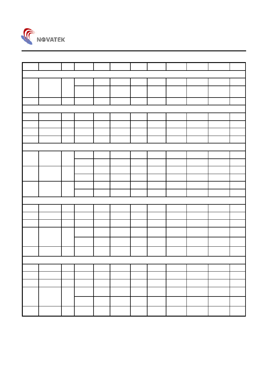
NT68P62-01
46
Control Register:
Addr
Register
INIT
Bit7
Bit6
Bit5
Bit4
Bit3
Bit2
Bit1
Bit0
R/W
Control Register for Polling Interrupt Groups
-
-
-
-
-
-
INTE0
INTMUTE
R
$0016
NMIPOLL
00H
-
-
-
-
-
-
CLRE0
CLRMUT
E
W
$0017
IRQPOLL
00H
-
-
-
-
-
IRQ2
IRQ1
IRQ0
R
Control Registers of Interrupt Enable
$0018
IENMI
00H
-
-
-
-
-
-
INTE0
INTMUTE
W
$0019
IEIRQ0
00H
-
-
INTS0
INTA0
INTTX0
INTRX0
INTNAK0
INTSTOP0
W
$001A
IEIRQ1
00H
-
-
INTS1
INTA1
INTTX1
INTRX1
INTNAK1
INTSTOP1
W
$001B
IEIRQ2
00H
-
-
-
-
-
INTV
INTE1
INTMR
W
Control Registers for Polling Interrupt Requests
-
-
INTS0
INTA0
INTTX0
INTRX0
INTNAK0
INTSTOP0
R
$001C
IRQ0
00H
-
-
CLRS0
CLRA0
CLRTX0
CLRRX0
CLRNAK0
CLRSTOP0
W
-
-
INTS1
INTA1
INTTX1
INTRX1
INTNAK1
INTSTOP1
R
$001D
IRQ1
00H
-
-
CLRS1
CLRA1
CLRTX1
CLRRX1
CLRNAK1
CLRSTOP1
W
-
-
-
-
INTADC
INTV
INTE1
INTMR
R
$001E
IRQ2
00H
-
-
-
-
CLRADC
CLRV
CLRE1
CLRMR
W
Control Register for DDC1/2B+ of Channel 0
$0021
CH0ADDR
A0H
ADR7
ADR6
ADR5
ADR4
ADR3
ADR2
ADR1
-
W
$0022
CH0TXDAT
00H
TX7
TX6
TX5
TX4
TX3
TX2
TX1
TX0
W
$0023
CH0RXDAT 00H
RX7
RX6
RX5
RX4
RX3
RX2
RX1
RX0
R
MD1/
-
START
STOP
-
-
W
$0024
CH0CON
E0H
-
-
START
STOP
-
-
-
R
$0025
CH0CLK
FFH
-
-
DDC2BR2 DDC2BR1
DDC2BR0
W
Control Register for DDC1/2B+ of Channel 1
$0026
CH1ADDR
A0H
ADR7
ADR6
ADR5
ADR4
ADR3
ADR2
ADR1
-
W
$0027
CH1TXDAT 00H
TX7
TX6
TX5
TX4
TX3
TX2
TX1
TX0
W
$0028
CH1RXDAT 00H
RX7
RX6
RX5
RX4
RX3
RX2
RX1
RX0
R
MD1/
-
START
STOP
-
-
W
$0029
CH1CON
E0H
-
-
START
STOP
-
-
R
$002A
CH1CLK
FFH
-
-
DDC2BR2
DDC2BR1 DDC2BR0
W

NT68P62-01
47
Last Comm,
is Repeat Start?
Send Address
Open INTTX INTNAK
Reset Buffer Index
Master Receiver
Recev. Over?
Send Address
Send Repeat Start
set last byte flag
Open INTRX & INTNAK
One Byte Data?
After Recv. Data
Send Repeat Start?
Send NO_ACK
Set Last Byte Flag
Send NO_ACK
Set Last Byte Flag
MODE = 0
Send Address
Open INTTX & INTNAK
Send Address
Send Repeat Start
Set Last Byte Flag
Open INTTX & INTNAK
One Byte Data?
After Recv. Data
Send Repeat Start?
Figure 15.9. Master Receiver Operation
Figure 15.10. Master Transmitter Operation
Last Comm,
is Repeat Start?
Send Address
Send Repeat Start
Open INTTX INTNAK
Reset buffer index
Master transmitter
Trans. Over?
MODE = 0
Send Address
Open INTTX & INTNAK

NT68P62-01
48
IRQ0/1 Group
Service Routine
Open INTRX & INTNAK INT
Read One Byte
Receiver Over
close INT interrupt
Read One Byte
Send repeat start
set last byte flag
Write 1 to MODE bit
(system send out a STOP)
Send repeat start
close INT interrupt
Figure 15.11. Master Mode INT Operation
Send repeat start
set last byte flag
Read One Byte
Write 1 to MODE bit
(system send out a STOP)
Put next byte data
CH0TXDATReg.
Open INTRX & INTNAK INT
Other interruptProcess
or Have someerror
No Slave Device Exist
System will send outSTOP &
set MODE bit to 1 automatically
Transmission failed

NT68P62-01
49
User Referenced Flow Chart
Comparison With NT68P61A
Item
NT68P61A Status
NT68P62 Status
Notes
Maximum ROM Size
24K Bytes
32K Bytes
RAM Size
256 Bytes
512 Bytes
PWM Channel
14 channels
5V & 12V Open Drain O/P
13 channels
5V Open Drain O/P Only
PWM Channel Refresh
Rate
31.25 KHz
62.5 KHz
A/D Converter Channel
2 channels
4 channels
6 bit resolution
V Counter Bit No.
12 Bits
(handle Vsync freq. down
to 30.5Hz)
14 Bits
(handle Vsync freq. down
to 7.6Hz)
H Interval
8.192 ms
16.384 & 32.768 ms
Auto Mute
X
O
Free Run Freq.
2 sets
5 sets
Self Test Pattern
X
O
2 self test patterns
IIC Bus Channel
1 channel
2 channels
IIC Bus Baud Rate
Max 100KHz
Max 400KHz
IIC Mode Supported
DDC1/2B
DDC1/2B+
External Interrupt
1 set
2 sets
NMI Interrupt
X
O
Interrupt Trigger Edge
Programmable
X
O
MASK ROM option
4K/8K/16K/24K
24K/32K
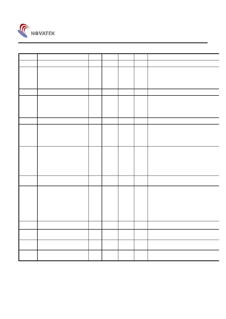
NT68P62-01
50
DC Electrical Characteristics
(V
DD
= 5V, T
A
= 25
�
C, Oscillator freq. = 8MHz, Unless otherwise specified)
Symbol
Parameter
Min.
Typ.
Max.
Unit
Conditions
I
DD
Operating Current
20
mA
No Loading
V
IH1
Input High Voltage
2
V
P00-P07, P12-P16,
P20-P27, P40, P41
, VSYNCI, HSYNCI, HALFHI INTE0,
INTE1
V
IH2
Input High Voltage
3
V
SCL0/1, SDA0/1,P10, P11, P30, P31 pins
V
IL1
Input Low Voltage
0.8
V
P00-P07, P12-P16,
P20-P27, P40, P41
, VSYNCI, HSYNCI, HALFHI,
INTE0, INTE1
V
IL2
Input Low Voltage
1.5
V
SCL0/1, SDA0/1, P10, P11 P30 ,P31 pins
I
IH
Input High Current
-200
-350
�
A
P00-P07, P10-P16,
P20-P27, P40,P41
VSYNCI, HSYNCI, HALFHI,
(V
IH
=2.4V);
V
OH1
Output High Voltage
2.4
V
P00-P07, P10-P16, P40,
P41 (I
OH
= -100
�
A)
VSYNCO, HSYNCO (I
OH
= -4mA)
HALFHO (I
OH
= -4mA)
PATTERN, P20-P27 (I
OH
= -10mA)
V
OH2
Output High Voltage
(DAC0-DAC12)
5
V
external applied voltage
V
OL
Output Low Voltage
0.4
V
P00-P07, P10-P16, P40,
P41, DAC0-12 (I
OL
= 4mA)
SCL0/1, SDA0/1 (I
OL
= 5mA)
VSYNCO, HSYNCO (I
OL
= 4mA)
HALFHO (I
OL
= 4mA)
PATTERN, P20-P27 ( I
OL
= 10mA)
R
OL
Pull Down Resistor (
)
50
100
150
K
R
OH1
Pull up Resistor
(INTE0, INTE1)
11
22
33
K
R
OH2
Pull up Resistor
(PORT0, PORT1, & PORT4)
11
22
33
K
R
OH3
Pull up Resistor
(HSYNCI & VSYNCI & HALFI)
11
22
33
K
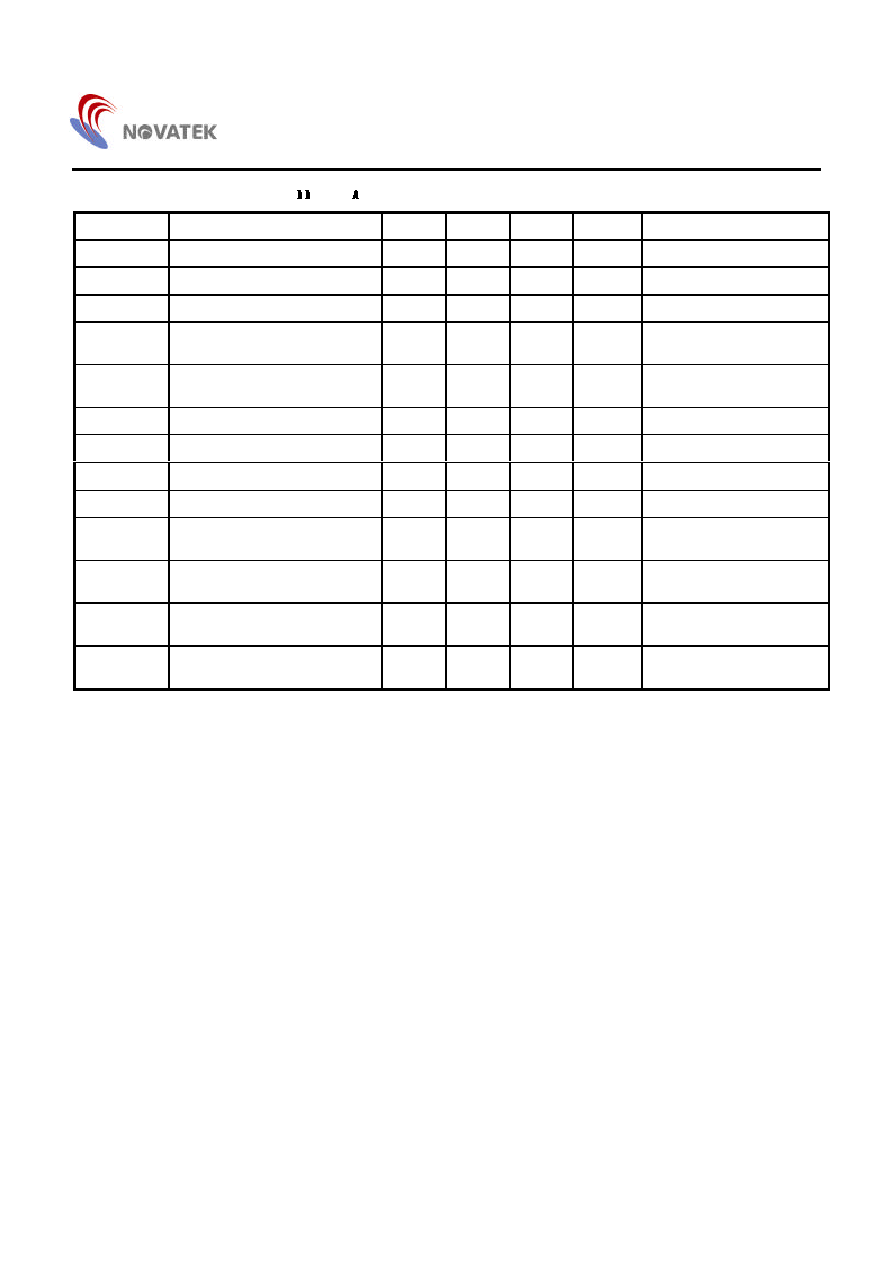
NT68P62-01
51
AC Electrical Characteristics
(V =5V, T =25
�
C, Oscillator freq.=8MHz, unless otherwise specified)
Symbol
Parameter
Min.
Typ.
Max.
Unit
Conditions
Fsys
System Clock
8
MHz
t
CNVT
A/D Conversion Time
750
�
s
Voffset
A/D Converter Error
1
LSB
Vlinear
A/D Input Dynamic Range of
Linearity Conversion
1.5
3.5
V
t
DELAY
The Delay Time of Vsync input
and Vsync output
20
ns
Composite sync with fixed
delay (Refer Figure 13.5)
t
RESET
Reset Pulse Width Low
2
t
CYCLE
t
CYCLE
= 2/ Fsys
Fvsync
Vsync Input Frequency
25K
Hz
t
VSYNC
= 1/Fvsync
t
VPW
Vsync Input Pulse Width
8
2000
�
s
Fhsync
Hsync Input Frequency
120
KHz
t
HSYNC
= 1/Fhsync
t
HPW1
Maximum Pulse Width of Hsync
Input High (Positive Polarity)
0.25
7
�
s
t
HPW2
Minimum Pulse Width of Hsync
Input Low (Positive Polarity)
9.125
�
s
t
ERROR1
Counting Deviation of Base
Timer
1
�
s
1
�
s clock source
t
ERROR2
Counting Deviation of Base
Timer
1
ms
1ms clock source
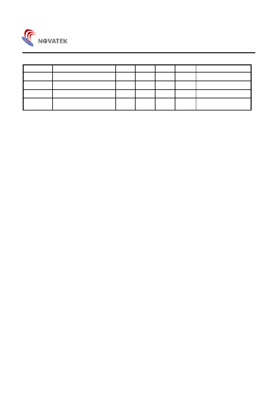
NT68P62-01
52
DDC1 Mode
Symbol
Parameter
Min.
Typ.
Max.
Unit
Conditions
t
VPW
Vsync High Time
0.50
2000
�
s
Fvsync
Vsync Input Frequency
25K
Hz
t
VSYNC
=1/Fvsync
t
DD
Data Valid
200
500
ns
t
MODE
Time for Transition to DDC2B
Mode
500
ns
Vsync Output
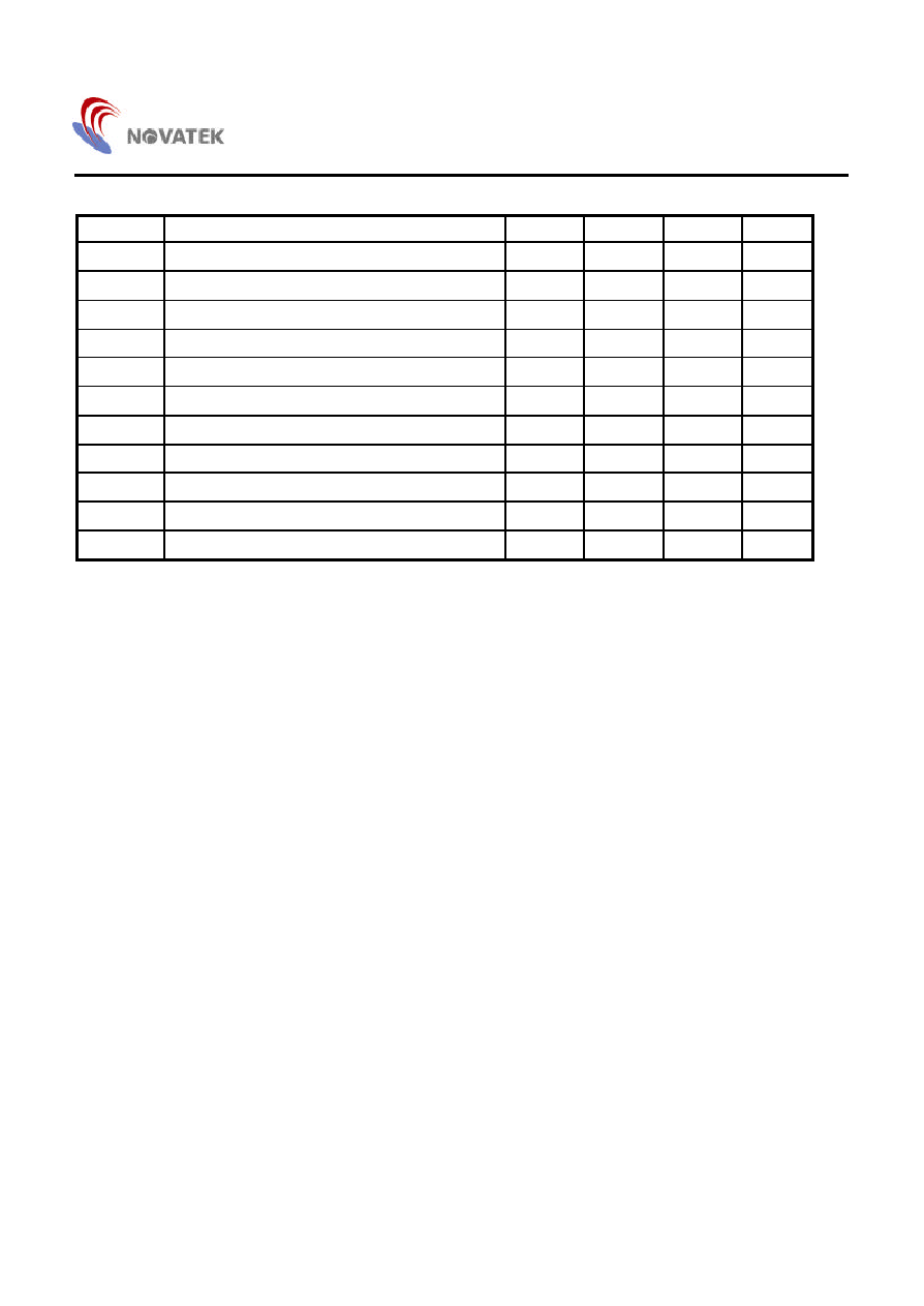
NT68P62-01
53
DDC2B+ Mode
Symbol
Parameter
Min.
Typ.
Max.
Unit
f
SCL
SCL Clock Frequency
400
KHz
t
BUF
Bus Free Between a STOP and START Condition
4.7
�
s
t
HD
; STA
Hold Time for START Condition
0.8
�
s
t
LOW
LOW Period of The SCL Clock
1.3
�
s
t
HIGH
HIGH Period of The SCL Clock
0.8
�
s
t
SU
; STA
Set-up Time for a Repeated START Condition
1.3
�
s
t
HD
; DAT
Data Hold Time
200
ns
t
SU
; DAT
Data Set-up Time
300
ns
t
R
Rise Time of Both SDA and SCL Signals
1
�
s
t
F
Fall Time of Both SDA and SCL Signals
300
ns
t
SU
; STO
Set-up Time for STOP Condition
0.80
�
s

NT68P62-01
54
Ordering Information
Part No.
Packages
NT68P62
40L P-DIP
NT68P62U
42L S-DIP
NT68P62-01
55
Package Information
P-DIP 40L Outline Dimensions
unit: inches/mm
Seating Plane
Symbol
Dimensions in inches
Dimensions in mm
A
0.210 Max.
5.33 Max.
A
1
0.010 Min.
0.25 Min.
A
2
0.155�0.010
3.94�0.25
B
0.018 +0.004
0.46 +0.10
-0.002
-0.05
B
1
0.050 +0.004
1.27 +0.10
-0.002
-0.05
C
0.010 +0.004
0.25 +0.10
-0.002
-0.05
D
2.055 Typ. (2.075 Max.)
52.20 Typ. (52.71 Max.)
E
0.600�0.010
15.24�0.25
E
1
0.550 Typ. (0.562 Max.)
13.97 Typ. (14.27 Max.)
e
1
0.100�0.010
2.54�0.25
L
0.130�0.010
3.30�0.25
0
�
~ 15
�
0
�
~ 15
�
e
A
0.655�0.035
16.64�0.89
S
0.093 Max.
2.36 Max.
Notes:
1. The maximum value of dimension D includes end flash.
2. Dimension E
1
does not include resin fins.
3. Dimension S includes end flash.

NT68P62-01
56
Package Information
S-DIP 42L Outline Dimensions
unit: inches/mm
Seating Plane
Symbol
Dimensions in inches
Dimensions in mm
A
0.200 Max.
5.08 Max.
A
1
0.020 Min.
0.51 Min.
A
2
0.157 Max.
4.0 Max.
b
0.051 Max.
1.3 Max.
0.031 Min.
0.8 Min.
b
1
0.021 Max.
0.53 Max.
0.016 Min.
0.40 Min.
c
0.013 Max.
0.32 Max.
0.010 Min.
0.23 Min.
D
(1)
1.531 Max.
38.9 Max.
1.512 Min.
38.4 Min.
E
(1)
0.551 Max.
14.0 Max.
0.539 Min.
13.7 Min.
e
0.070
1.778
e
1
0.600
15.24
L
0.126 Max.
3.2 Max.
0.114 Min.
2.9 Min.
M
E
0.622 Max.
15.80 Max.
0.600 Min.
15.24 Min.
M
H
0.675 Max.
17.15 Max.
0.626 Min.
15.90 Min.
w
0.007
0.18
Z
(1)
0.068 Max.
1.73 Max.
Notes:
1. Plastic or metal protrusions of 0.25 mm maximum per side are not included.