357 Beloit Street, P.O. Box 457, Burlington, WI 53105-0457 U.S.A. Phone 262/763-3591 FAX 262/763-2881
Email:
nelsales@nelfc.com
www.nelfc.com
Data Sheet 0635A
CRYSTAL OSCILLATORS
OC-X87XXXXX Series
Micro-miniature OCXO
Features
∑
Low Cost DIL 14 package
∑
High Vacuum Sealed Crystal
∑
Low Power Consumption (500 mW)
∑
Fast Warm-up Time (2 minutes)
∑
Stratum3 or better Stability
∑
Low Aging < 3 ppm over life
∑
Very Low Phase Noise (-160dBc/Hz TYP)
∑
HCMOS/TTL or Sine-Wave output
∑
8 MHz to 160 MHz Frequencies Available
∑
Voltage Control Optional
Applications
∑
Telecommunications
∑
Data Communications
∑
Instrumentation
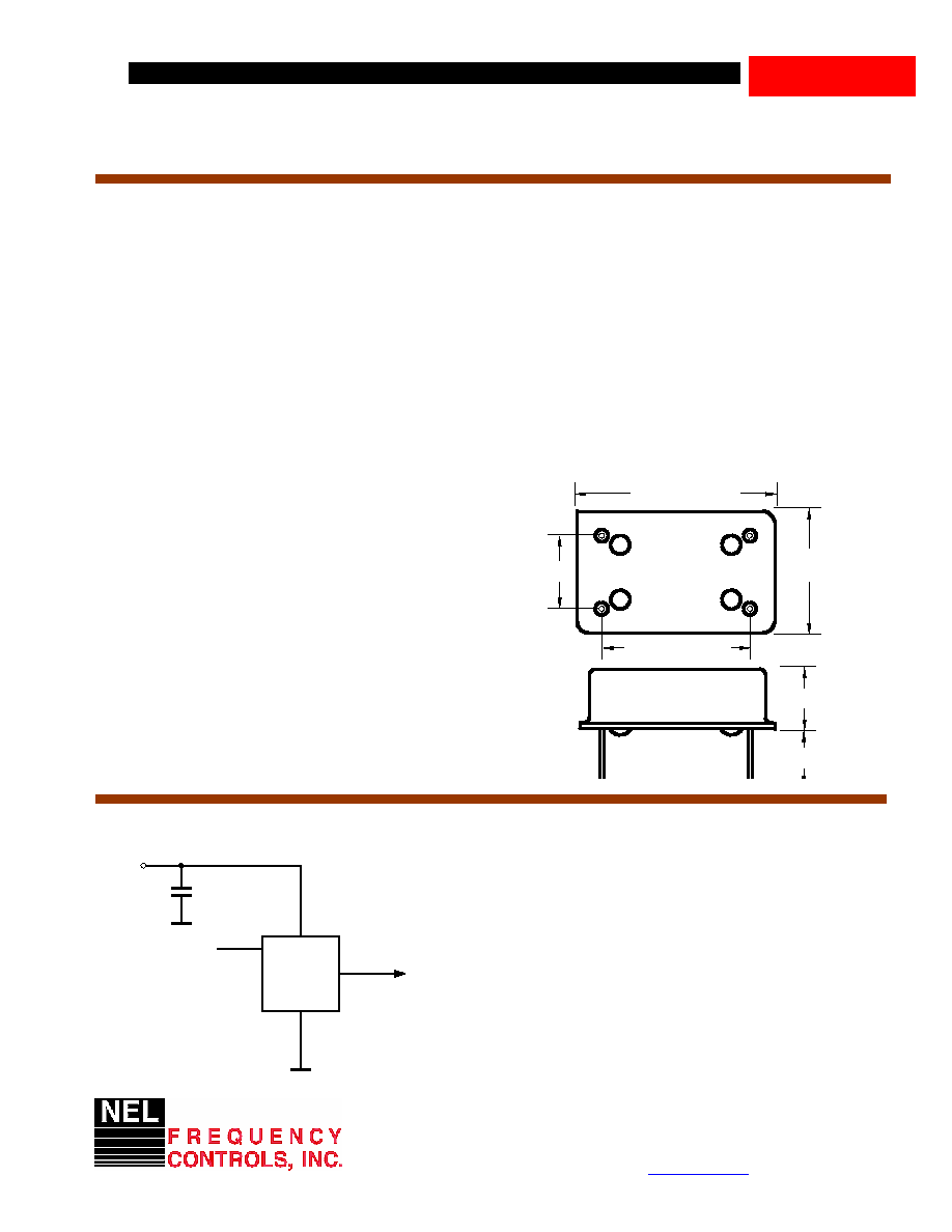
7
DUT
Vc
14
1
Vcc
OUTPUT
8
0.340 (8.7 mm)
0.250 (6.2 mm)
7
8
14
1
0.300 (7.6 mm)
0.500 (12.7 mm)
0.800 (20.3 mm)
0.600 (15.2mm)
357 Beloit Street, P.O. Box 457, Burlington, WI 53105-0457 U.S.A. Phone 262/763-3591 FAX 262/763-2881
Email:
nelsales@nelfc.com
www.nelfc.com
Data Sheet 0635A
CRYSTAL OSCILLATORS
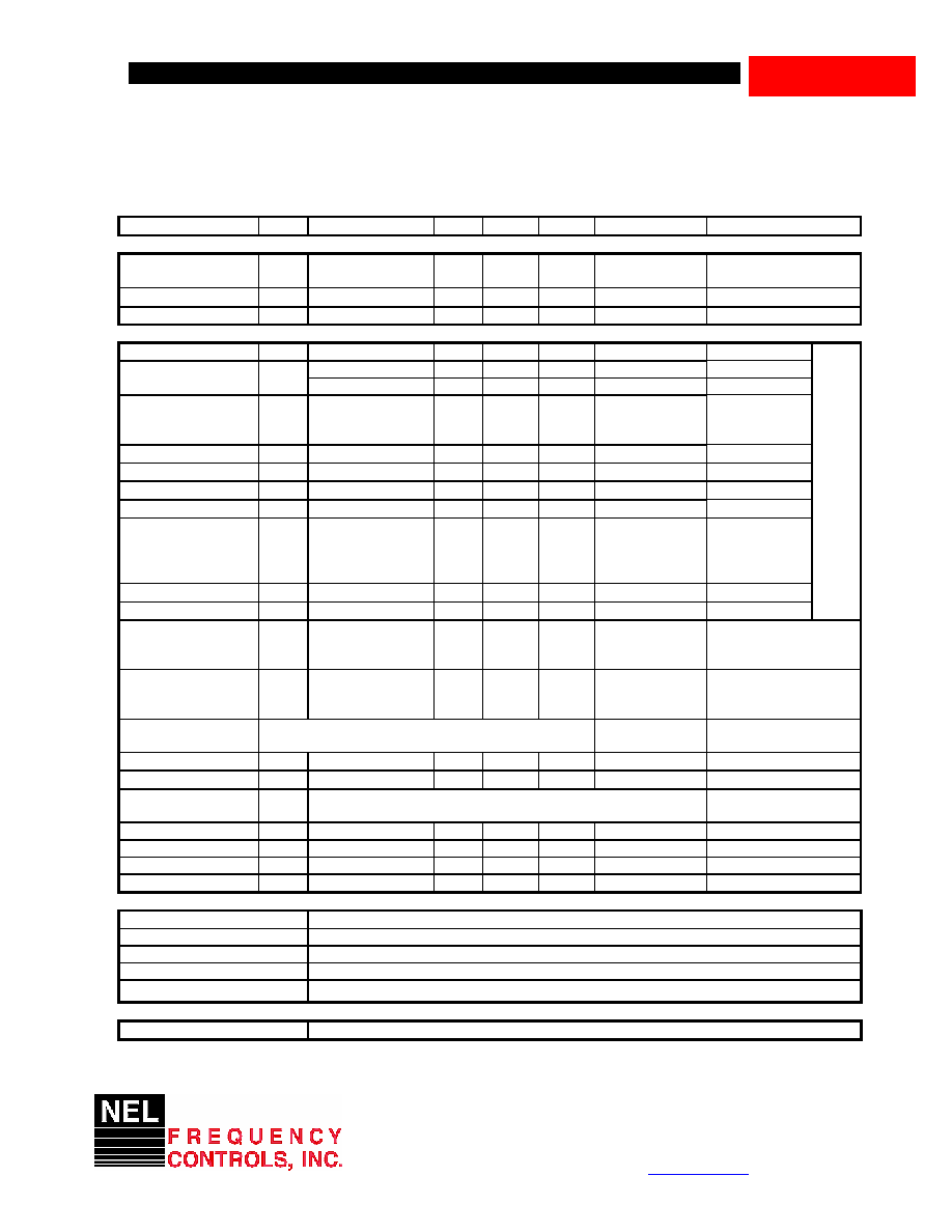
Specifications:
OC-X87XXXXX Series
Micro-miniature OCXO
Parameter Symb
Condition
Min
Typ
Max
Unit
Note
Absolute Maximum Ratings
Input Break
Down Voltage
Vcc -0.5
-0.5
5.5
13
V
3.3V or 5V Vcc
12 V Vcc
Storage temper.
Ts -40
85
∞C
Control Voltage
Vc -1
6 V
Electrical
Frequency
F 8
10.000
160
MHz 1*
vs. Temp.
±100
±280
ppb
See chart below
Frequency stability
F/F
vs. Supply
10
50
ppb/V
Aging
per day
first year
15 years
5E-9
3E-7
3E-6
after 30 days
Allan Variance
.1s to 100s
5E-11
Calibration
No voltage control
± 0.5
± 2
ppm
Vcc sensitivity
5E-8/V
Load sensitivity
For 10% change
5E-8
SSB Phase Noise
10 Hz
100 Hz
1 KHz
>10 KHz
-100
-130
-145
-160
dBc/Hz
2*
Retrace
After 30 minutes
±100
ppb
G-sensitivity
worst direction
±2.0
ppb/G
Al
l
p
a
ramet
ers fo
r 1
0
M
H
z
Input Voltage
Vcc 4.75
3.15
11.4
5.0
3.3
12.0
5.25
3.45
12.6
V
See chart below
Power consumption
P
steady state, 25∞C
steady state, -30∞C
start-up
0.5
0.7
1.5
2.5
W Upper
operating
temperature < 70∞C, add
20% for UOT 85∞C
Load
10KOhm//15pF
Internally AC coupled 50 Ohm
CMOS
Output
Sine-wave output
Warm-up time
to 0.3 ppm accuracy
2
3
min
Sub-Harmonics
-50
-40
dBc
At higher F 1*
Output Waveform
3.3V HCMOS/TTL compatible, 4 ns Tr/Tf, 40/60% duty cyicle
Sine-wave, + 7 dBm ±3 dBm into 50 Ohm, -30 dBc harmonics
See chart below
Control voltage
Vc 0
4.0
V
Pull range
from nominal F
±5
±10
ppm
Customer specified
Deviation slope
Monotonic,
posit 5
ppm/V
Customer
specified
Setability
Vc0
@25∞C, Fnom.
1.0
2.0
3.0
V
5V/3.3 supply
Environmental and Mechanical
Operating temp. range
-30∞C to 70∞C Standard, Other options ≠ see chart below
Mechanical Shock
Per MIL-STD-202, 30G, 11ms
Vibration
Per MIL-STD-202, 5G to 2000 Hz
Soldering Conditions
Leads Temperature 260∞C, for 10s, Max
Hermetic Seal
Leak rate less than 1x10⁻⁸ atm.ccm/s of helium
Electrical Connections
Pin Out
Pin 1- Vc; Pin 7- Case, GND; Pin8 ≠ Output; Pin 14 - Vcc

357 Beloit Street, P.O. Box 457, Burlington, WI 53105-0457 U.S.A. Phone 262/763-3591 FAX 262/763-2881
Email:
nelsales@nelfc.com
www.nelfc.com
Data Sheet 0635A
CRYSTAL OSCILLATORS
OC-X87XXXXX Series
Micro-miniature OCXO
OC ≠ X 87 X X XX X
Package Code
OC 0.8x0.5" 4pin (14pin)
Creating a Part Number
FREQUENCY, MHz
Temperature Range
Code Specification
A
0∞C to 50∞C
B -10∞C
to
60∞C
C
0∞C to 70∞C
D -20∞C
to
70∞C
E -30∞C
to
70∞C
F -40∞C
to
85∞C
Temperature Stability
Code Specification
05 5x10
-8
10 1x10
-7
28 2.8x10
-7
30 3x10
-7
50 5x10
-7
YZ YZx10
-8
Supply Voltage
Code Specification
0
5V ± 5%
A 3.3V
±
5%
F 12V
±
5%
Not all combinations are available. Consult Factory
.
Notes:
1* Higher frequencies can be achieved either by using higher frequency crystals or by low noise analog harmonic
multiplication. Both methods have advantages and drawbacks. If lowest possible phase noise on the noise floor is most important ≠
high frequency crystal will be used. If phase noise close to the carrier and aging are more important ≠ multiplication will be used.
Please consult factory for your specific requirement.
2* Phase noise deteriorates with frequencies going higher. If analog multiplication is used to achieve higher frequency the
phase noise roughly follows the formula of additional 20LogN, where N is a multiplication factor across entire frequency offset range.
If higher frequency is achieved by using higher frequency crystal phase noise close to the carrier deteriorates due to the lower Q of the
crystal and is usually worse, compared to multiplied solution. On the noise floor, however it remains more or less the same.
Output
Code Specification
T TTL/
CMOS
S Sine
Voltage Control
Code Specification
V Voltage
Control
0 No
Voltage
Control