 | –≠–ª–µ–∫—Ç—Ä–æ–Ω–Ω—ã–π –∫–æ–º–ø–æ–Ω–µ–Ω—Ç: OLF300 | –°–∫–∞—á–∞—Ç—å:  PDF PDF  ZIP ZIP |

Description
Features
ISO
LINK
SCHEMATIC
PACKAGE OUTLINE
Hermetic SMT package
Electrical parameters guaranteed over
-55
∞
C to +125
∞
C ambient temp. range
1000 Vdc electrical isolation
High-Speed, 1 Mbit/s typical
Open collector output
300 Khz bandwidth
Similar to 6N135/136, 4N55
Radiation tolerant
100% hi-rel screenings are offered
The OLF300 is suitable for interfac-
ing TTL to LSTTL, TTL or CMOS as well
as wide bandwidth analog applications.
Each OLF300 has a light emitting diode
and an integrated photo-diode transistor
detector mounted and coupled in a cus-
tom 8-pin hermetic flat pack package
providing 1000 Vdc electrical isolation
between input and output. The integrated
photo-diode transistor improves switching
speed by orders of magnitude as com-
pared to standard photo transistors, by
reducing the base to collector capaci-
tance. The internal shield provides excel-
lent common-mode immunity perfor-
mance.
1. Measured between pins 1, 2 and 6 shorted together and pins 3, 4, and 5 shorted together. T
A
=25
∞
C and duration = 1 second.
2. Current transfer ratio is defined as the ratio of output collector current, Ic to the forward LED current, I
F
, times 100%.
NOTES:
OLF300
High-Speed
Hermetic Surface Mount
Optocoupler
1
2
3
4
5
6
7
8
.015±.002
.050 BSC
.180 SQ. MAX
.200 MIN.
.004/.006
.100 MAX.
.030±.005
SEATING PLANE
OLF XXX
XXYY
S
VCC
VOUT
CATHODE
ANODE
2
1
GND
5
Shield
6
8
VB
7

ELECTRICAL CHARACTERISTIC ( T
A
= - 55
∞
C to +125
∞
C, Unless Otherwise Specified )
I
F
=16 mA, V
O
=0.4 V, V
CC
=4.5 V
I
F
=0mA, V
O
=V
CC
=15V
I
F
=10mA, V
CC
=15V, V
O
=open
I
F
=0mA, V
CC
=15V, V
O
=open
I
F
=10 mA
I
R
=10
µ
A
Relative Humidity
45%,
T
A
= 25
∞
C, V
I - O
= 1000 Vdc
I
F
=16 mA, Vcc= 5V,
R
L
=8.2 K
,C
L
=50pF
I
F
=0, R
L
=8.2K
,VCM=10V p-p
I
F
=16, R
L
=8.2K
,VCM=10V p-p
Parameter
Symbol Min Typ. Max Units Test Conditions Fig. Note
100
200
10
2.5
1.0
2.0
6.0
2
1
3,4
3,4
2
1
25
.05
40
.05
1.7
0.3
0.8
>1
>1
9
3
CTR
I
OH
I
CCL
I
CCH
V
F
B
VR
I
I - O
t
PHL
t
PLH
CM
H
CM
L
Current Transfer Ratio
Logic High Output Current
Logic Low Supply Current
Logic High Supply Current
Input Forward Voltage
Input Reverse
BreakdownVoltage
Input to Output
Leakage Current
Propagation Delay Time
LogicHigh to Low
Logic Low to High
Common Mode Trasient
immunity
Logic High Level
Logic Low Level
%
µ
A
µ
A
µ
A
V
V
µ
A
µ
S
µ
S
KV
KV
ALL TYPICAL @ T
A
= 25
∞
C
Absolute Maximum Ratings
±
1000 Vdc
-65
∞
C to +150
∞
C
-55
∞
C to +125
∞
C
240
∞
C
20 mA
40 mA
5.0 V
36 mW
8 mA
16 mA
-0.5 V to 18 V
-0.5 V to 18 V
50 mW
Coupled
Input to Output Isolation Voltage
1
Storage Temperature Range
Operation Temperature Range
Lead Temperature 1.6 mm from case for 10 sec.
Input Diode
Average Input Current
Peak Forward Current (
1mS duration )
Reverse Voltage
Power Dissipation
Output Detector
Average Output Current
Peak Output Current
Supply Voltage, Vcc
Output Voltage, Vout
Power Dissipation
1.5 V
t
PLH
t
PHL
INPUT I
F
V
OUT
V
OL
I
F
= 10 mA
PULSE
GENERATOR
Zo =50
tr = 5ns
10% D.C.
100µS=P.W.
I
F
Monitor
R
L
+ 5V
Vo
100
I
F
CL=15pf
Shield
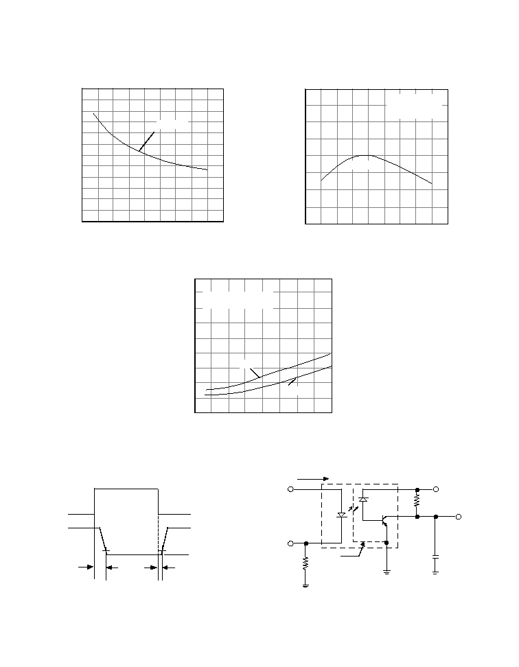
Fig. 4 - Switching Test Circuit
TYPICAL PERFORMANCE CURVES
AMBIENT TEMPERATURE (∞C)
FORWARD VOLTAGE (V)
I
F
= 16 mA
Fig. 1 -
LED Forward Characteristics
1.2
1.4
1.6
1.8
2.0
2.2
Fig. 2
- Normalized Output Current
vs. I
F
vs. Temperature
150
125
100
75
50
25
0
-25
-50
-75
0.2
0.4
0.6
0.8
1.0
1.2
1.4
1.6
1.8
NORMALIZED OUTPUT CURRENT
AMBIENT TEMPERATURE (∞C)
NORMALIZED TO :
I
F
= 16 mA
T
A
= 25 ∞C
I
F
= 16 mA
Fig. 3 -
Propagation Delay vs.
Temperature
125
100
75
50
25
0
-25
-50
-75
AMBIENT TEMPERATURE (∞C)
0
0.2
0.4
0.6
0.8
1.0
1.2
1.4
1.6
1.8
PROPAGATION DELAY (µS)
I
F
= 16 mA, R
L
= 8.2 k
V
CC
= 5 V
t
PLH
t
PHL