 | –≠–ª–µ–∫—Ç—Ä–æ–Ω–Ω—ã–π –∫–æ–º–ø–æ–Ω–µ–Ω—Ç: OM9369CM | –°–∫–∞—á–∞—Ç—å:  PDF PDF  ZIP ZIP |

8 10 R2
Supersedes 6 11 R1
FULL-FEATURED POWER MODULE FOR HIGH-VOLTAGE
DIRECT DRIVE OF 3-PHASE BRUSHLESS DC MOTORS
FEATURES
∑
Fully integrated 3-Phase Brushless DC Motor Control Subsystem
includes power stage, non-isolated driver stage, and controller stage
∑
Rugged IGBT Power Output Stage with Soft Recovery Diode
∑
25A Average Phase Current with 300V Maximum Bus Voltage
∑
Internal Precision Current Sense Resistor (6W max. dissipation)
∑
Speed and Direction Control of Motor
∑
Brake Input for Dynamic Braking of Motor
∑
Overvoltage/Coast Input for Shutdown of All Power Switches
∑
Soft Start for Safe Motor Starting
∑
Unique Lightweight Hermetic Ceramic-to-Metal Sealed Module (CERMOD
TM
)
∑
(4.255" x 2.475" x .74")
APPLICATIONS
∑
Fans and Pumps
∑
Hoists
∑
Actuator Systems
DESCRIPTION
The OM9369CM is one of a series of versatile, integrated three-phase brushless DC motor
controller/driver subsystems housed in a CERMOD
TM
. The OM9369CM is best used as a two
quadrant speed controller for controlling/driving fans, pumps, and motors in applications which require
small size. Typical size brushless DC motors that the OM9369CM can effectively control range from
fractional HP up to several HP. The OM9369CM is ideal for use on DC distribution busses up to and
including 270Vdc. Many integral control features provide the user much flexibility in adapting the
OM9369CM to specific system requirements.
The small size of the complete subsystem is ideal for aerospace, military, and high-end industrial
applications.
OM9369CM
205 Crawford Street, Leominster, MA 01453 USA (978) 534-5776 FAX (978) 537-4246
Visit Our Web Site at www.omnirel.com
25 Amp. Push-Pull 3-Phase Brushless
DC Motor Controller/Driver Module
in a Ceramic-to-Metal Sealed Module
P R E L I M I N A R Y

COMMUTATION TRUTH TABLE
This table shows the Phase Output state versus
the state of the Hall-Effect and Direction Inputs.
Please note that the OM9369CM Hall-Effect
Inputs are Grey-encoded; that is, only one input
is allowed to change from one input state to
another at a time.
The commutation coding shown reflects Hall-
Effect sensors that are spaced at 120
∞
mechanical increments. Also, internal
protection logic disables all three Phase
Outputs when the Hall-Effect Inputs are set to
an illegal condition (i.e. all logic low or all logic
high).
2.1 - 2
SIMPLIFIED BLOCK DIAGRAM
OM9369CM
VCC (1)
Ground (20)
EA1+ (5)
Hall_1 (23)
Hall_2 (22)
Hall_3 (21)
Direction (25)
OV_Coast (18)
Tach_Out (16)
V_Motor (B)
Phase_A (E)
Phase_C (C)
EA1- (3)
EA1_Out (9)
EA2+ (4)
EA2- (7)
EA2_Out (8)
PWM_In (10)
Osc (11)
+5V_Ref (6)
Quad_Sel (15)
I_Sense (12)
ISH (13)
ISL (14)
CSL (27)
CSH (26)
Phase_B (D)
Pwr_Gnd (A)
Delay (2)
RC_Brake (17)
Speed_In (24)
SStart (19)
R/C
R/C
Filter
High-Side/
Low-Side
Drivers
with Bootstrap
and Charge Pump
High-Side/
Drivers
Low-Side
with Bootstrap
Low-Side
with Bootstrap
and Charge Pump
High-Side/
Drivers
and Charge Pump
Startup
Circuit
Vcc
Tach_Out
Tach_Out
V_Ref
Vcc
V_Ref
Quad_Sel
OV_Coast
Quad_Sel
OV_Coast
ISH
ISL
ISH
ISL
Delay
Delay
RC_Brake
RC_Brake
SStart
SStart
+
-
+
-
R_Sense
UC1625
RC_OSC
25
GND
15
E/A_IN(+)
1
E/A_OUT
27
PWM_IN
26
E/A_IN(-)
28
VREF
2
H1
8
H2
9
H3
10
DIR
6
RC_BRAKE
21
QUAD_SEL
22
OV_COAST
23
VCC
19
PWR_VCC
11
SSTART
24
PUA
18
PUC
16
PUB
17
PDC
12
PDB
13
PDA
14
ISENSE_1
4
ISENSE_2
5
SPEED_IN
7
ISENSE
3
TACH_OUT
20
DIGITAL INPUTS
PHASE OUTPUTS
Dir
H1
H2
H3
A
B
C
1
0
0
1
Hi-Z
Sink
Source
1
0
1
1
Sink
Hi-Z
Source
1
0
1
0
Sink
Source
Hi-Z
1
1
1
0
Hi-Z
Source
Sink
1
1
0
0
Source
Hi-Z
Sink
1
1
0
1
Source
Sink
Hi-Z
0
1
0
1
Sink
Source
Hi-Z
0
1
0
0
Sink
Hi-Z
Source
0
1
1
0
Hi-Z
Sink
Source
0
0
1
0
Source
Sink
Hi-Z
0
0
1
1
Source
Hi-Z
Sink
0
0
0
1
Hi-Z
Source
Sink
X
0
0
0
Hi-Z
Hi-Z
Hi-Z
X
1
1
1
Hi-Z
Hi-Z
Hi-Z

2.1 - 3
OM9369CM
ABSOLUTE MAXIMUM RATINGS
Motor Supply Voltage, V
m
. . . . . . . . . . . . . . . . . . . . . . . . . . . . . . . . . . . . . . . . . . . . . . . . . . 300 Vdc
Peak Motor Supply Voltage V
m pK
. . . . . . . . . . . . . . . . . . . . . . . . . . . . . . . . . . . . . . . . . . . 500 Vdc
Average Phase Output Current, I
o
. . . . . . . . . . . . . . . . . . . . . . . . . . . . . . . . . . . 25 Amperes DC*
Peak Phase Output Current, I
om
. . . . . . . . . . . . . . . . . . . . . . . . . . . . . . . . . . . 50 Amperes Peak**
Control Supply Voltage, V
cc
. . . . . . . . . . . . . . . . . . . . . . . . . . . . . . . . . . . . . . . . . . . . . . . . . . .
+
18 V
Logic Input Voltage
(Note 1
) . . . . . . . . . . . . . . . . . . . . . . . . . . . . . . . . . . . . . . . . . . . . -0.3 V to +8 V
Reference Source Current . . . . . . . . . . . . . . . . . . . . . . . . . . . . . . . . . . . . . . . . . . . . . . . . -30 mAdc
Error Amplifier Input Voltage Range, (EA1+/EA1-) . . . . . . . . . . . . . . . . . . . . -0.3 Vdc to 10 Vdc
Error Amplifier Output Current . . . . . . . . . . . . . . . . . . . . . . . . . . . . . . . . . . . . . . . . . . . . . . ±8 mAdc
Spare Amplifier Input Voltage (EA2+/EA2-). . . . . . . . . . . . . . . . . . . . . . . . . . . -0.3 Vdc to 10 Vdc
Spare Amplifier Output Current . . . . . . . . . . . . . . . . . . . . . . . . . . . . . . . . . . . . . . . . . . . . . ±8 mAdc
Current Sense Amplifier Input Voltage (ISH/ISL) . . . . . . . . . . . . . . . . . . . . . . . -0.3 V to +6 Vdc
Current Sense Amplifier Output Current . . . . . . . . . . . . . . . . . . . . . . . . . . . . . . . . . . . . . ±10 mAdc
Tachometer Output Current . . . . . . . . . . . . . . . . . . . . . . . . . . . . . . . . . . . . . . . . . . . . . . . . ±10 mAdc
PWM Input Voltage . . . . . . . . . . . . . . . . . . . . . . . . . . . . . . . . . . . . . . . . . . . . . . - 0.3 Vdc to +6 Vdc
Operating Junction Temperature . . . . . . . . . . . . . . . . . . . . . . . . . . . . . . . . . . . . . -55∞C to +150∞ C
Storage Temperature Range . . . . . . . . . . . . . . . . . . . . . . . . . . . . . . . . . . . . . . . . -65∞ C to +150∞ C
Power Switch Junction-to-Case Thermal Resistance, R
jc
. . . . . . . . . . . . . . . . . . . . . . 0.48∞C/W
Package Isolation Voltage . . . . . . . . . . . . . . . . . . . . . . . . . . . . . . . . . . . . . . . . . . . . . . . . . 600 Vrms
Lead Soldering Temperature . . . . . . . . . . . . . 300∞C, 10 seconds maximum, 0.125" from case
* Tcase = 25∞ C
** Tcase = 25∞ C, Maximum pulse width = 10mSec
RECOMMENDED OPERATING CONDITIONS
(Tcase = 25∞ C)
Motor Power Supply Voltage, V
m
. . . . . . . . . . . . . . . . . . . . . . . . . . . . . . . . . . . . . . . . . + 2 7 0 Vdc
Average Phase Output Current, I
O
With Internal Current Sense Resistor
(Note 2)
Each Power Switch . . . . . . . . . . . . . . . . . . . . . . . . . . . . . . . . . . . . . . . . . . . . . 25 A
Control Supply Voltage, V
cc
. . . . . . . . . . . . . . . . . . . . . . . . . . . . . . . . . . . . . . . . . . . . 15Vdc ±10%
Logic Low Input Voltage, V
il
. . . . . . . . . . . . . . . . . . . . . . . . . . . . . . . . . . . . . . . . . . . 0.8 Vdc (max)
Logic High Input Voltage, V
ih
. . . . . . . . . . . . . . . . . . . . . . . . . . . . . . . . . . . . . . . . . . . 2.0 Vdc (min)
Note 1: Logic Inputs: Direction, Hall Inputs (H1...H3) Overvoltage - Coast, Speed, and Quad Select.
Note 2: The internal 5m
current sense resistor is limited to 6 Wdc power dissipation. Other values are available.
Please contact the factory for more information.
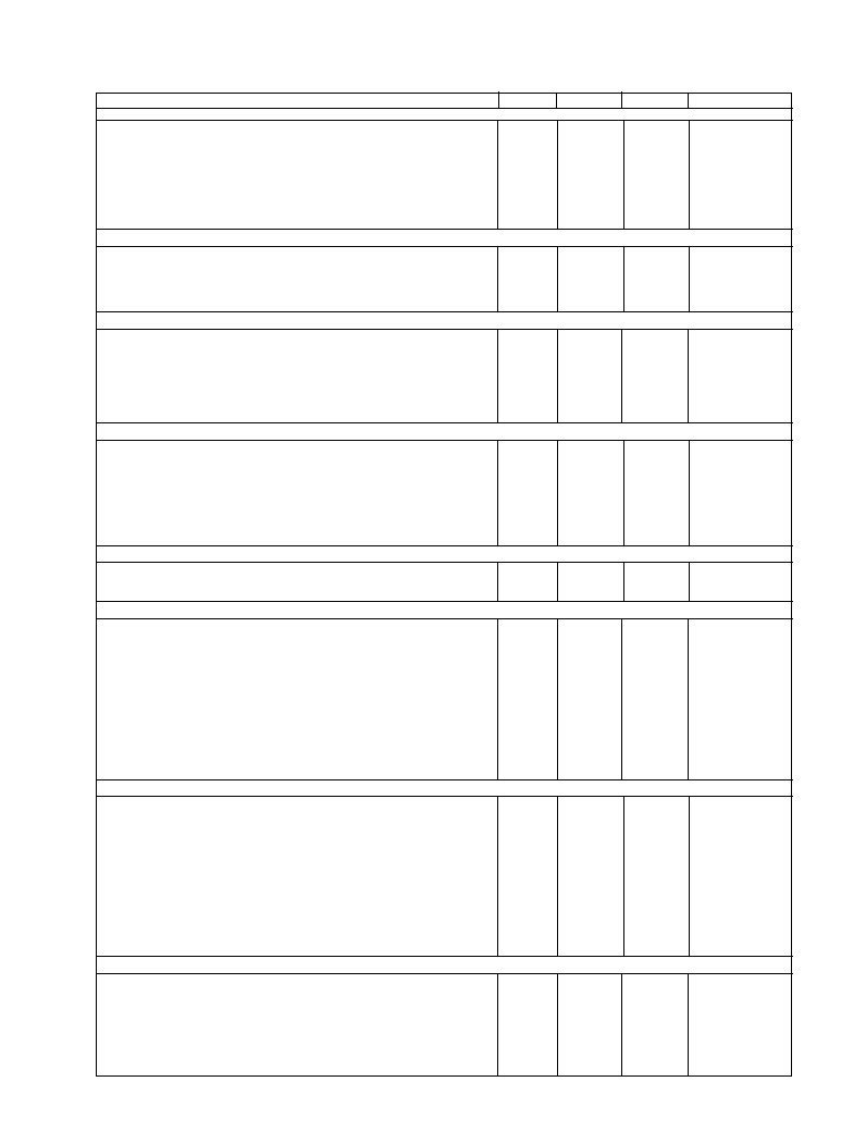
PARAMETER
SYMBOL
CONDITIONS (NOTE 1)
MIN.
TYP.
MAX.
UNITS
Power Output Section
IGBT Leakage Current
Ices
Vce = 600Vdc
300
uA
Vge = 0V
IGBT c-e Saturation Voltage
Vce(sat)
Ic = 50Adc
3.2
V
Vge = 15V
Diode Leakage Current
Ir
Vr = 600Vdc
100
uA
Diode Forward Voltage
Vf
If = 37A
1.7
V
Diode Reverse Recovery Time
trr
Io = 1A, di/dt = -100A/usec,
50
ns
Vr = 30V
Control Section
Control Supply Current
Icc
Vcc over operating range
100
mA
Control Turn-On Threshold
Vcc(+)
Tc over operating range
9.45
V
Driver Turn-On Threshold
Vcc(+)
Tc over operating range
13.0
V
Reference Section
Output Voltage
Vref
4.9
5.0
5.1
V
Output Voltage
Vref
Tc over operating range
4.7
5.0
5.3
V
Output Current
Io
---
---
30
mA
Load Regulation
Iload = 0mA to -20mA
-40
-5
mV
Short Circuit Current
Isc
Tc over operating range
50
100
150
mA
Error Amplifier / Spare Amplifier Sections
EA1 / EA2 Input Offset Current
Ios
V(pin 3) = V(pin 5) = 0V
-30
-3
0
nA
V(pin 4) = V(pin 7) = 0V
EA1 / EA2 Input Bias Current
Iin
V(pin 3) = V(pin 5) = 0V
-50
-45
0
nA
V(pin 4) = V(pin 7) = 0V
Input Offset Voltage
Vos
0V < Vcommon-mode < 3V
7
mV
Amplifier Output Voltage Range
--
0
6
V
PWM Comparator Section
PWM Input Current
Iin
V(pin 10) = 2.5V
0
3.0
30
uA
Current-Sense Amplifier Section
ISH / ISL Input Current
Iin
V(pin 13) = V(pin 14) = 0V
-850
-320
0
uA
Input Offset Current
Ios
V(pin 13) = V(pin 14) = 0V
+/-2
+/-12
uA
Peak Current Threshold Voltage
Vpk
V(pin 13) = 0V, V(pin 14)
0.14
0.20
0.26
V
Varied to Threshold
Over Current Threshold Voltage
Voc
V(pin 13) = 0V, V(pin 14)
0.26
0.30
0.36
V
Varied to Threshold
ISH / ISL Input Voltage Range
--
(Note 2)
-1
2
V
Amplifier Voltage Gain
Av
V(pin 13) = 0.3V, V(pin 14)
1.75
1.95
2.15
V/V
= 0.5V to 0.7V
Amplifier Level Shift
--
V(pin 13) = V(pin 14) = 0.3V
2.4
2.5
2.65
V
Logic Input Section
H1, H2, H3 Low Voltage Threshold
Vil
Tc over operating range
0.8
1.0
1.2
V
H1, H2, H3 High Voltage Threshold
Vih
Tc over operating range
1.6
1.9
2.0
V
H1, H2, H3 Input Current
Iin
Tc over operating range,
-400
-250
-120
uA
V(pin 21, 22 or 23) = 0Vdc
Quad Select / Direction
Threshold Voltage
Vth
Tc over operating range
0.8
1.4
2.0
V
Quad Select Voltage Hysteresis
Vh
70
mV
Direction Voltage Hysteresis
Vh
0.6
V
Quad Select Input Current
Iin
-30
50
150
uA
Direction Input Current
Iin
-30
-1
30
uA
Overvoltage / Coast Input Section
Overvoltage / Coast Inhibit
Threshold Voltage
Vth
Tc over operating range
1.65
1.75
1.85
V
Overvoltage / Coast Restart
Threshold Voltage
Vth
Tc over operating range
1.55
1.65
1.75
V
Overvoltage / Coast Hysteresis Voltage Vh
0.05
0.10
0.15
V
Overvoltage / Coast Input Current
Iin
-10
-1
0
uA
2.1 - 4
OM9369CM
ELECTRICAL CHARACTERISTICS

Parameter
Symbol
Conditions (Note 1)
MIN.
TYP.
MAX.
Units
Soft-Start Section
Soft-Start Pull-Up Current
Ip
V(pin 19) = 0V
-16
-10
-5
uA
Soft-Start Discharge Current
Id
V(pin 19) = 2.5V
0.1
0.4
3.0
mA
Soft-Start Reset Threshold Voltage
Vth
0.1
0.2
0.3
V
Tachometer/Brake Section
Tachometer Output High Level
Voh
Tc o
ver operating range
4.7
5.0
5.3
V
(Pin 16) 10k
to 2.5 V
Tachometer Output Low Level
Vol
Tc o
ver operating range
(Pin 16) 10k
to 2.5 V
0.2
V
Tachometer On-Time
ton
85
100
140
us
Tachometer On-Time Variation
--
Tc o
ver operating range
0.1
%
Brake/Tach Timing Input Current
Iin
V (pin 17) = oV
-4.0
-1.9
mA
Brake/Tach Timing
Threshold Voltage
Vth
Tc o
ver operating range
0.8
1.0
1.2
V
Brake/Tach Timing
Voltage Hysteresis
Vh
0.09
V
Speed Input Threshold Voltage
Vth
Tc o
ver operating range
220
257
290
mV
Speed Input Current
Iin
-30
-5
30
uA
Oscillator Section
Oscillator Frequency
fo
Measured at pin 11
13.5
14.8
20.0
kHz
SPECIFICATION NOTES:
1. All parameters specified for Ta = 25
∞
C, Vcc = 15Vdc, Rosc = 75K
(to Vref), Cosc = 1800 pF, and all Phase Outputs unloaded (Ta ~ Tj). All negative currents shown
are sourced by (flow from) the pin under test.
2. Either ISH or ISL may be driven over the range shown.
3. Bold parameters tested at -55
∞
C, 25
∞
C, 125
∞
C.
PIN#
NAME
PIN#
NAME
1
VCC
24
Speed Input
2
Delay
25
Direction Input
3
EA1 "-" Input
26
CSH
4
EA2 "+" Input
27
CSL
5
EA1 "+" Input
28
(No Connection)
6
+5V Reference Output
A
Motor Return
7
EA2 "-" Input
B
Vmotor
8
EA2 Output
C
Phase C Output
9
EA1 Output
D
Phase B Output
10
PWM Input
E
Phase A Output
11
Oscillator Timing Input
(Base)
(No Connection)
12
Isense
13
ISH
14
ISL
15
Quad Select Input
16
Tachometer Output
17
Brake/Tach Timing Input
18
Overvoltage/Coast Input
19
Soft-Start Input
20
Ground
21
H3 Input
22
H2 Input
23
H1 Input
2.1 - 5
OM9369CM
PINOUT