 | –≠–ª–µ–∫—Ç—Ä–æ–Ω–Ω—ã–π –∫–æ–º–ø–æ–Ω–µ–Ω—Ç: OM9551SP | –°–∫–∞—á–∞—Ç—å:  PDF PDF  ZIP ZIP |
OM9551SP, OM9552SP, OM9553SP, OM9554SP
Rev A
08/01/2000
205 Crawford Street
∑ Leominster MA 01453 ∑ Phone: 978 534 5776 ∑ Fax: 978 537 4246 ∑ www.omnirel.com
1
5V Input,
3A Output Current
+3.3V, +2.5V +1.8V, +1.5V Output
Switching Regulator
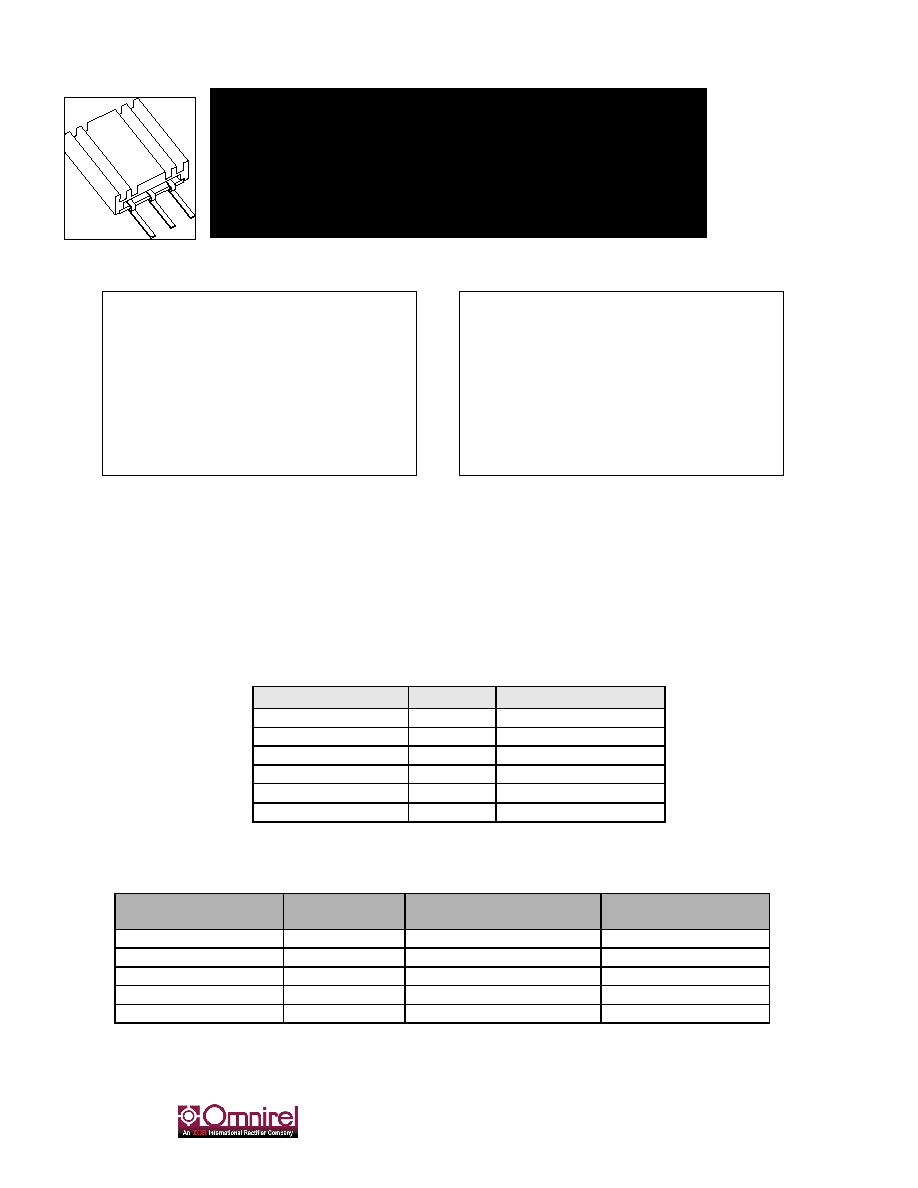
Three Terminal Package
DESCRIPTION
The OM955X series of Switching Regulators are designed for pin compatibility with standard 3-
Pin linear regulators. They are well suited for on-board, non- isolated power applications where
efficient point- of- load regulation is needed. The package is designed using Chip- on ≠ Board
technology to reduce cost and maintain power density. These units will typically not require any
additional components in your application due to capacitance provided internal to the package.
MAXIMUM RATINGS @ Ta=25
∞ C (unless otherwise specified)
Parameter
Value
Conditions
Input Voltage
8V
Output Current
4A
Short Circuit
Power Dissipation
1.8W
Short Circuit
Output Power
10W
Short Circuit
Lead Temp.
230
∞C
< 1 min.
CONFIGURATION CHART
MODEL
OUTPUT
VOLTAGE
TEMPERATURE RANGE
MAX. OUTPUT
CURRENT
OM9551SP 3.3V -25 to +85
∞
∞
∞
∞C
3.0A
OM9552SP 2.5V -25 to +85
∞
∞
∞
∞C
3.0A
OM9553SP 1.8V -25 to +85
∞
∞
∞
∞C
3.0A
OM9554SP 1.5V -25 to +85
∞
∞
∞
∞C
3.0A
FEATURES
∑
High Efficiency
∑
Internal Short Circuit Protection
∑
Small Footprint
∑
High Power Density- 60W/in.
3
APPLICATIONS
∑
High Power 5V to 3.3V Regulation
∑
Low Voltage Battery regulation
∑
Embedded Processor Power
∑
General Purpose Low Voltage Logic
Supply
∑
FPGA Power

OM9551SP, OM9552SP, OM9553SP, OM9554SP
Rev A
08/01/2000
205 Crawford Street
∑ Leominster MA 01453 ∑ Phone: 978 534 5776 ∑ Fax: 978 537 4246 ∑ www.omnirel.com
2
PERFORMANCE CHARACTERISTICS (Ta= 25
∞
∞
∞
∞C)
INPUT
Parameter
Symbol
Test Conditions
MIN
MAX
Units
Line Regulation
Rline
4.5V
Vin 5.5V
-0.5 +0.5 %
Input Voltage
Range
Vin
4.5 7.0 V
Input Filtering
1
22
uF
OUTPUT
Parameter
Symbol
Test Conditions
MIN
TYP
MAX
Units
Power
Po
Vo= 3.3V
10
W
Vout Accuracy
Vo
Vo= 3.3V, +2.5V,
+1.5V+1.8V
0.8
1.0
%
Vout Regulation
Vreg
Vin= 5V, 0.1
I3A 0.3
0.1
%
Output Ripple
V
Vin= 5V, Io= 3.0A
80
100
mV(p-p)
Current Limiting
Ilim
Vin= 5V
4.0
A
Efficiency
Vin=5V,Io=3A,Vo=+3.3V
88
%
Efficiency
Vin=5V,Io=3A,Vo=+2.5V
87
%
Efficiency
Vin=5V,Io=3A,Vo=+1.8V
86
%
Efficiency
Vin=5V,Io=3A,Vo=+1.5V
85
%
Min. Load Current Il(min)
0.1
A
Output Filter
Capacitance
1
Co All
Models
330
uF
DYNAMIC
Parameter
Test Conditions
MIN
TYP
MAX
Units
Transient
Response
50% load step
Vout
40
200
µ
µ
µ
µS
mV
Frequency
0 to 85
∞
∞
∞
∞C
175 200 225
KHz
ENVIRONMENTAL
Parameter
MODEL
MIN
MAX
Units
Operating
Temperature
OM9551SP,
OM9552SP,
OM9553SP,
OM9554SP
-25 85
∞
∞
∞
∞C
Storage Temp.
-40
125
∞
∞
∞
∞C
Flammability
UL94V0
1
Included in the package
OM9551SP, OM9552SP, OM9553SP, OM9554SP
Rev A
08/01/2000
205 Crawford Street
∑ Leominster MA 01453 ∑ Phone: 978 534 5776 ∑ Fax: 978 537 4246 ∑ www.omnirel.com
3
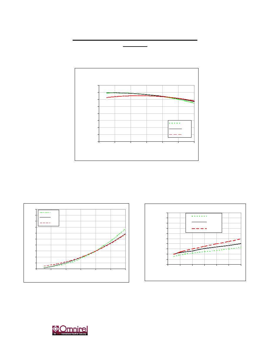
Typical Performance Characteristics
(Ta= 25
∞
∞
∞
∞C)
Vo= +3.3V
Pow er Dissipation vs Output Current
0.00
0.20
0.40
0.60
0.80
1.00
1.20
1.40
1.60
1.80
2.00
0.00
0.50
1.00
1.50
2.00
2.50
3.00
Iout (A)
PD (W)
4.5V
5.0V
5.5V
Efficiency vs Output Current
Vo= +3.3V
60.00
65.00
70.00
75.00
80.00
85.00
90.00
95.00
100.00
0.00
0.50
1.00
1.50
2.00
2.50
3.00
Iout (A)
Efficiency (%)
4.5V
5.0V
5.5V
Ripple vs Output Curre nt
0.00
20.00
40.00
60.00
80.00
100.00
120.00
140.00
160.00
180.00
200.00
0.00 0.50 1.00 1.50 2.00 2.50 3.00
Iout (A)
Ripple (mV)
4.5V
5.0V
5.5V

OM9551SP, OM9552SP, OM9553SP, OM9554SP
Rev A
08/01/2000
205 Crawford Street
∑ Leominster MA 01453 ∑ Phone: 978 534 5776 ∑ Fax: 978 537 4246 ∑ www.omnirel.com
4
MECHANICAL OUTLINE
Package Pinout
Vout
GND
Vin

OM9551SP, OM9552SP, OM9553SP, OM9554SP
Rev A
08/01/2000
205 Crawford Street
∑ Leominster MA 01453 ∑ Phone: 978 534 5776 ∑ Fax: 978 537 4246 ∑ www.omnirel.com
5
APPLICATION CIRCUIT
Internal to the package is a 22uF input capacitor and a 330uF output capacitor.
The Omnirel process allows sufficient space allocation to include all components
necessary to complete the basic regulation design. The additional by-pass
capacitors are suggested if an improvement in switching noise becomes necessary.
COM
OM9551SP
1
2
3
COM
Vin(+4.5- 5.5)
Vout(+)
(optional)
(optional)
0.1uF
0.1uF
(3.3V)