 | –≠–ª–µ–∫—Ç—Ä–æ–Ω–Ω—ã–π –∫–æ–º–ø–æ–Ω–µ–Ω—Ç: OMC507 | –°–∫–∞—á–∞—Ç—å:  PDF PDF  ZIP ZIP |

9 04 R0
FULL-FEATURED CIRCUIT BOARD ASSEMBLY FOR
DIRECT DRIVE OF 3-PHASE BRUSHLESS DC MOTO R S
F E AT U R E S
∑ Fully integrated 3-Phase Brushless DC Motor Control System
∑ 5A Average Phase Current (10A peak) with 30V Maximum Bus Voltage
∑ Onboard Current Sense Resistor
∑ Direction and Torque Control
∑ Tachometer Output
∑ Fits Inside Motor Housing
APPLICATIONS
∑ Fans and Pumps
∑ Hoists
∑ Actuator Systems
DESCRIPTION
The OMC507 is a three phase brushless DC Motor Controller Driver. The OMC507 is a 2
quadrant controller and provides control of motor current (torque) in proportion to the input
current command. The versatility of the OMC507 allows the user to either provide an analog
or a TTL PWM current command signal externally, or to set an analog current command
onboard. The OMC507 also allows the user to adjust the current command offset onboard
through the use of a potentiometer. Loop compensation is provided onboard and loop
compensation component values can be modified to meet specific customer requirements,
thereby optimizing the controller for each application.
The OMC507 controller utilizes surface mount and through hole technology. The OMC507
is a mere 2 1/2 inches in diameter and can fit inside the motor housing. A connector for the
control section is optional; consult the factory.
OMC507
205 Crawford Street, Leominster, MA 01453 USA (978) 534-5776 FAX (978) 537-4246
Visit Our Web Site at www.omnirel.com
5 Amp. Push-Pull 3-Phase Brushless
DC Motor Controller/Driver Circuit Board

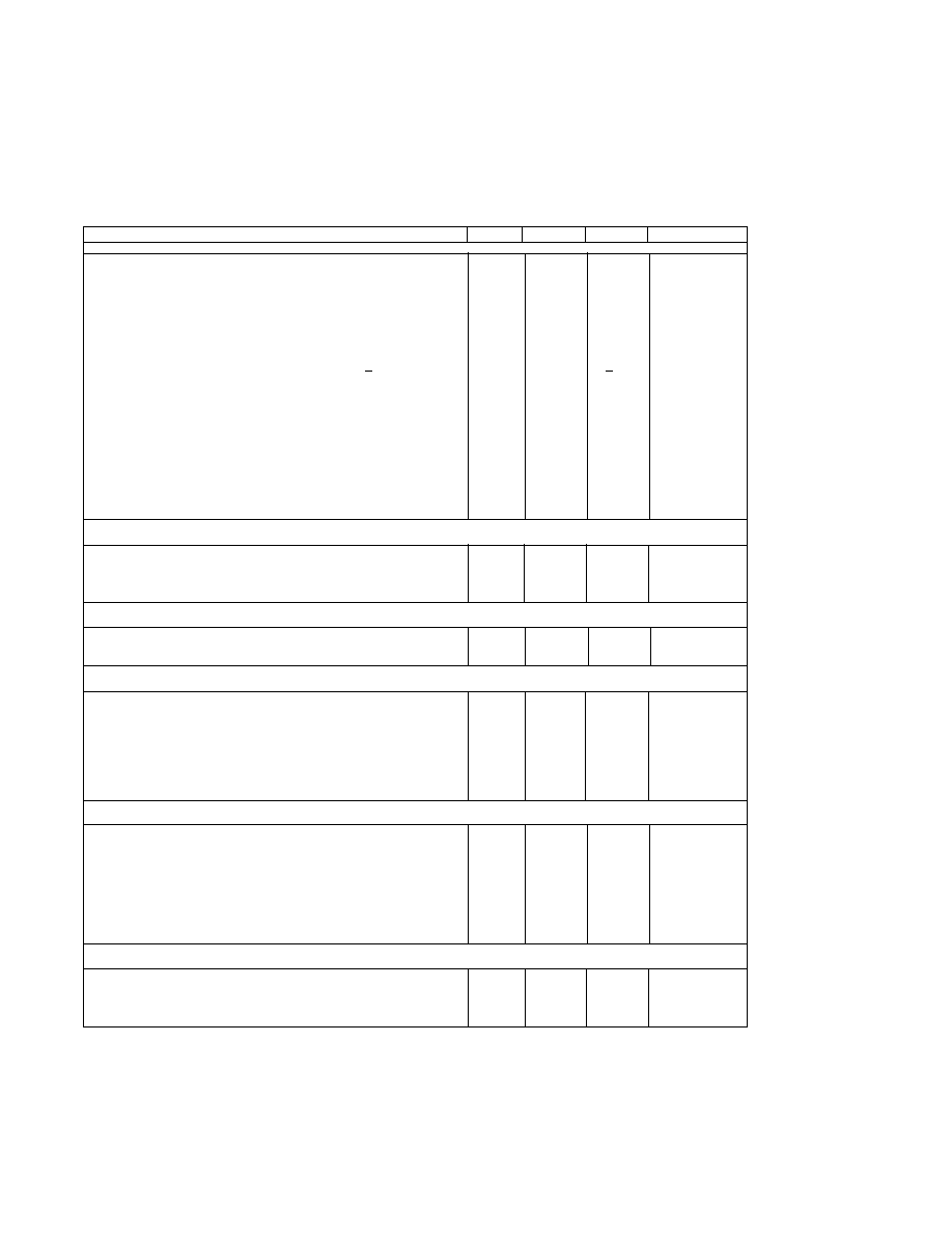
C O M M U TATION TRUTH TA B L E
This table shows the Phase Output state versus
the state of the Hall-Effect and Direction Inputs.
Please note that the Hall-Effect Inputs are
Grey-encoded; that is, only one input is allowed
to change from one input state to another at a
time.
The commutation coding shown reflects Hall-
Effect sensors that are spaced at 120
mechanical increments. Also, internal
protection logic disables all three Phase
Outputs when the Hall-Effect Inputs are set to
an illegal condition (i.e. all logic low or all logic
high).
DIGITAL INPUTS
PHASE OUTPUTS
Dir
H1
H2
H3
A
B
C
1
0
0
1
Hi-Z
Sink
Source
1
0
1
1
Sink
Hi-Z
Source
1
0
1
0
Sink
Source
Hi-Z
1
1
1
0
Hi-Z
Source
Sink
1
1
0
0
Source
Hi-Z
Sink
1
1
0
1
Source
Sink
Hi-Z
0
1
0
1
Sink
Source
Hi-Z
0
1
0
0
Sink
Hi-Z
Source
0
1
1
0
Hi-Z
Sink
Source
0
0
1
0
Source
Sink
Hi-Z
0
0
1
1
Source
Hi-Z
Sink
0
0
0
1
Hi-Z
Source
Sink
X
0
0
0
Hi-Z
Hi-Z
Hi-Z
X
1
1
1
Hi-Z
Hi-Z
Hi-Z
2.1 - 2
SIMPLIFIED BLOCK DIAGRAM
O M C 5 0 7
Vcc (1)
Ground (2)
Command (5)
+5V
+5V_Hall (6)
Hall_A (8)
Hall_B (9)
Hall_C (10)
Direction (11)
Enable (12)
Tach_Out (13)
V_Motor
Phase_A
Phase_B
Phase_C
Monitor (14)
Vcc
VREF
VREF
Tach_Out
Tach_Out
Vcc
Bus
Bus
Bus
Bus
VREF
U1
UC3625
25
15
1
27
26
28
2
8
9
10
6
21
22
23
19
11
24
18
16
17
12
13
14
4
5
7
3
20
RC_OSC
GND
E/A_IN(+)
E/A_OUT
PWM_IN
E/A_IN(-)
VREF
H1
H2
H3
DIR
RC_BRAKE
QUAD_SEL
OV_COAST
VCC
PWR_VCC
SSTART
PUA
PUC
PUB
PDC
PDB
PDA
ISENSE_1
ISENSE_2
SPEED_IN
ISENSE
TACH_OUT
R_Sense
C_Bus
10uF
R/C
Compensation
Network
R/C
Voltage
Regulator
Enable
Level
Shift
Level
Shift
Level
Shift
Filter
Circuit
Offset
Adjust
Set/Adjust
Command

2.1 - 3
O M C 5 0 7
ABSOLUTE MAXIMUM RATINGS
Motor Supply Voltage, V
m
................................................... 30 Vdc
Peak Motor Supply Voltage V
m pK
............................................. 50 Vdc
Average Phase Output Current, I
o
@ T
A
= +25
∞ C ........................ 5 Amperes DC
I
o
@ T
A
= +85
∞ C ....................... 3 Amperes DC
Peak Phase Output Current, I
o pk
@ T
A
= +25
∞ C...................... 10 Amperes Peak*
Control Supply Voltage, V
cc
...................................................
+
18 V
Logic Input Voltage
(Note 1
) ............................................ -0.3 V to +6 V
Reference Source Current ................................................ -30 mAdc
Command Input Voltage Range, ....................................... -0.3 V to +6 V
Current Sense Amplifier Input Voltage (ISH/ISL) ....................... -0.3 V to +6 Vdc
Tachometer Output Current ................................................ ±10 mAdc
Operating Ambient Temperature ....................................... 0∞ C to +85∞ C
Operating Junction Temperature ...................................... 0∞ C to +120∞ C
Storage Temperature Range ........................................ -20∞ C to +120∞ C
Power Switch Junction-to-Ambient Thermal Resistance, Rq
jA
................... 62.5∞C/W
*Maximum pulse width = 10 Sec
R E C O M M E N D E D O P E R ATING CONDITIONS
(T
A
= 25∞ C)
Motor Power Supply Voltage, V
m
........................................... + 2 8 Vdc
Average Phase Output Current, I
O (Note 2)
......................................... 5 A
Control Supply Voltage, V
cc
............................................ 15Vdc ±10%
Logic Low Input Voltage, V
i
l
........................................... 0.8 Vdc (max)
Logic High Input Voltage, V
i
h
........................................... 2.0 Vdc (min)
Note 1: Logic Inputs: Direction, Hall Inputs (Hall_A...Hall_C), and Enable.
Note 2: Onboard current sense resistor; 20 m (nominal), 2W.
Parameter
Symbol
Conditions (Note 1)
MIN.
TYP.
MAX.
Units
Power Output Section
Zero Gate Voltage Drain Current
Idss
(N-CH) Vds = 60Vdc
1
µA
Vgs = 0V
(P-CH) Vds = -60Vdc
-1
µA
Vgs = 0V
Drain-to-Source On-Resistance
Rds(on)
(N-CH) Id =30 A
0.008
O h m s
Vgs = 10V (Note 2)
(P-CH) Id =-30 A
0.020
O h m s
Vgs = -10V (Note 2)
Gate Body Leakage Current
Igss
Vgs = + 20 Vdc
+ 100
nA
Vds = 0V
Diode Forward Voltage
V
S D
(N-CH)I
F
= 30 A (Note 2)
0.9
V
Vgs = 0V
(P-CH) I
F
= -30 A
-1.0
V
Vgs = 0V
Diode Reverse Recovery Time
t
r
r
(N-CH)I
F
=75 A,
120
nSec
di/dt = 100A/usec,
Vgs = 0V
(P-CH) I
F
= -65 A
120
nSec
di/dt = 100A/usec,
Vgs = 0V
Control Section
Control Supply Current
Icc
Tc over operating range
100
m A
Control Turn-On Threshold
Vcc(+)
Tc over operating range
9.45
V
Reference Section
Output Voltage
Vref
4.9
5.0
5.1
V
Output Current
Io
30
m A
Current-Sense Amplifier Section
Peak Current Threshold Voltage
Vpk
V(pin 12) = 0V, V(pin 13)
0.14
0.20
0.26
V
Varied to Threshold
Over Current Threshold Voltage
Voc
V(pin 12) = 0V, V(pin 13)
0.26
0.30
0.36
V
Varied to Threshold
Amplifier Voltage Gain
Av
V(pin 12) = 0.3V, V(pin 13)
1.75
1.95
2.15
V/V
= 0.5V to 0.7V
Amplifier Level Shift
-
-
V(pin 12) = V(pin13) = 0.3V
2.4
2.5
2.65
V
Logic Input Section
H1, H2, H3 Low Voltage Threshold
Vil
Tc over operating range
0.8
1.0
1.2
V
H1, H2, H3 High Voltage Threshold
Vih
Tc over operating range
1.6
1.9
2.0
V
H1, H2, H3 Input Current
I
i
n
Tc over operating range,
-400
-250
-120
uA
V(pin 8, 9 or 10) = 0Vdc
Direction Threshold Voltage
Vth
Tc over operating range
0.8
1.4
2.0
V
Direction Voltage Hysteresis
Vh
0.6
V
Direction Input Current
I
i
n
-30
-1
30
uA
Enable Input Section
Enable Threshold Voltage
Vth
2.0
V
Enable Input Current
I
i
n
100
uA
2.1 - 4
O M C 5 0 7
ELECTRICAL CHARACTERISTICS (Note 1)

Parameter
Symbol
Conditions (Note 1)
MIN.
TYP.
MAX.
Units
Command Input Section
Command Input Voltage Range
V
C M
0
5
V
Tachometer/Brake Section
Tachometer Output High Level
Voh
Tc o
ver operating range
4.7
5.0
5.3
V
Tachometer Output Low Level
Vol
Tc o
ver operating range
0.2
V
Tachometer On-Time
ton
85
100
140
us
Tachometer On-Time Variation
-
-
Tc o
ver operating range
0.1
%
Oscillator Section
Oscillator Frequency
fo
10.5
kHz
SPECIFICATION NOTES:
1. All parameters specified for Ta = 25 C, Vcc = 15Vdc, and all Phase Outputs unloaded (Ta ~ Tj). All negative currents shown are sourced by (flow from) the pin under
test.
2. Pulse Test: Pulse width < 300 µsec, duty cycle < 2%.
2.1 - 5
O M C 5 0 7
PINOUT
PIN#
N A M E
J1-1
V C C
J1-2
Ground
J1-3
N/C
J1-4
N/C
J1-5
Command
J1-6
+5V_Hall
J1-7
Hall_Rtn
J1-8
Hall_A
J1-9
Hall_B
J1-10
Hall_C
J1-11
Direction
J1-12
Enable
J1-13
Tach_Out
J1-14
Offset_Mon
T1
V_Motor
T2
Motor_Rtn
T3
Phase_A
T4
Phase_B
T5
Phase_C