
OR43300 DATA SHEET
Rev 2.1
December 10, 2001
Page 1
Company Confidential
www.oren.com
OR43300
Video Ghost Canceller / Adaptive Equalizer
DATA SHEET
G
ENERAL
D
ESCRIPTION
The OR43300 is a video-rate adaptive equalizer IC that reduces the effect of multi-path signal echoes
(ghosts). The IC uses a proprietary algorithm to dramatically improve the received image quality of NTSC
or PAL broadcasts. The device's internal 576-tap digital filter eliminates artifacts that result from multi-
path echoes including multiple images, color distortion, and image smearing.
The OR43300 performs all the functions required for ghost cancellation, eliminating the need for external
DSP controllers, memory, sync detection, D/A converters, A/D converters, and user programming.
ROM versions of the device are available which operate entirely from internal memory and which meet the
unique requirements of differing GCR standards. ROM versions are denoted by the last two digits of the
device part number and the following suffix.
F
EATURES
Implements NTSC & PAL ghost cancellation
Compatible with all international ghost
canceller reference (GCR) standards
Capable of `blind' equalization, using Teletext
signals as reference
Internal 576-tap digital filter
Internal adaptive equalizer DSP with
embedded software for digital filter coefficient
calculation
Up to four different Roll Off Curves available
for different reception conditions
Internal 10-bit A/D converter with
programmable clamp position
Internal 10-bit D/A converter with
programmable gain and offset
Cancellation of �6.15 �S precursor ghosts
through +41.6 �S post-cursor ghosts
Cancellation of �6dB ghosts
Ghost residue down to -40dB
Convergence time 1.7 to 11.2 seconds
Improved algorithms for cancellation in noisy
reception conditions
Digital Output option designed for direct
interface with 3D Y/C separators, includes
offset and scaling
I
2
C serial port for host processor interface
Reports available through I
2
C include SNR and
equalizer taps
NCO circuit enables wide range of crystal
input frequencies
Accepts externally generated reference clock
2.8V to 3.3V supply
TTL compatible interface, 5V tolerant
Low cost 80-pin plastic QFP package
1.3W maximum power consumption

OR43300 DATA SHEET
Rev 2.1
December 10, 2001
Page 2
Company Confidential
www.oren.com
GC
Bypass
Delay
Digital
GC Filter
Adder
10
10
Offset
Scalar
8
Gain
Adder
10
10
Offset
Scalar
8
Gain
10
Clock
Ref
PLL
NCO
ADC
Master
Clock
Gen
Gain
Clamp
9
DAC
MUX
MUX
DSP
Controller
and
Processor
Microcode
ROM / RAM
Data RAM
I2C
Interface
Boot ROM
Interface
Sync
Seperator
Analog
CVBS
Input
Digital
CVBS
Input
OR43300
Boot ROM
(Optional)
System
Controller
Digital
CVBS
Output
Clock Input
Analog
CVBS
Output
Alternate Clock Source:
Genlocked clock provided by digital video
circuit that accepts CVBS from OR43300
Figure 1: OR43300 System Architecture
1. Functional Description
1.1 The Ghosting Problem
Broadcast television signals reflected from buildings, mountains, and other objects create time shifted
and attenuated echoes (ghosts) of the originally transmitted signal. Ghosts are characterized by their
occurrence in time and by their amplitude, both with respect to the main signal. Those arriving before the
main energy signal, known as precursor ghosts, are created when the main energy signal is reflected and
is delayed relative to other distorted versions of the signal. Those arriving after the main energy signal,
the typical case, are known as post-cursor ghosts.
Since TV transmitters for different stations may be widely separated, ghost characteristics vary greatly
from channel to channel. In addition, the multi-path characteristics for each channel can change over
time. As a result, an adaptive digital filter is required to cancel multi-path ghosts in all possible
transmission environments. Ghost cancellation requires that a "training" signal be added to the signal of
interest to provide a reference signal for adaptation of filter coefficients.
1.2 The Ghost Cancellation Reference Signal
In 1993, the FCC approved a Ghost Canceller Reference (GCR) signal for broadcast by television
stations in the United States. This reference signal is added to the conventional National Television
Systems Committee (NTSC) base band signal. The United States GCR is inserted into the NTSC signal
in each field at line 19 of the vertical blanking interval (VBI). This same reference signal has also been
approved for broadcast in Canada, and a PAL version of the GCR has been approved for broadcast in
Brazil, New Zealand, and Australia.
Japan, Korea, and Taiwan have each adopted unique GCR standards. Many other countries are actively
evaluating GCR signals. The OR43300 is compatible with all GCR signal standards.
NOTE: A THIRD PARTY LICENSE MAY BE REQUIRED TO USE GCR SIGNALS.

OR43300 DATA SHEET
Rev 2.1
December 10, 2001
Page 3
Company Confidential
www.oren.com
1.3 Overview
The OR43304 576-tap internal digital filter cancels ghosts occurring from -6.15
�
s before to +41.6
�
s
after the main signal. The digital filter is comprised of a 144-tap finite impulse response (FIR) section
which its first 88 taps reduce precursor ghosts and a 432-tap recursive filter section that eliminates post-
cursor ghosts. The 432-tap recursive filter section is further divided into a 360-tap main filter block that
eliminates all post-cursor ghosts occurring from 0 to +25
�
s after the main signal, and two 36-tap
"floating" filter blocks that remove rare ghosts occurring from +25
�
s to +41.6
�
s after the main signal.
The OR43300 cancels ghosts with signal strength of -6dB relative to the main video signal, leaving a
ghost residue down to -40dB relative to the main signal.
-6.15
�
�
�
�
s
No. of Taps:
+3.9
�
�
�
�
s
+25
�
�
�
�
s
delay
56
88
304
36 delay 36
+41.6
�
�
�
�
s
FIR/IIR Overlap
Post-Cursor
Ghosts
Pre-Cursor
Ghosts
Main Video Signal
Figure 2: OR43300 Internal Filter Structure
Note: Ghost coverage times are for NTSC. In PAL systems the coverage is extended (~3%)
A central DSP unit controls all modes of operation and executes the processing algorithms. On-chip
memory stores the algorithm microcode and standard GCR waveform. In the OR43300, the on-chip
memory is RAM which is boot loaded through the I
2
C serial port or from external EPROM through
parallel port. ROM versions of the device are also available that operate entirely from internal memory.
In Bypass mode,
the digital value of the video input is passed unaltered to the output stage with
the same latency as in Ghost Cancellation mode. Bypass mode is activated upon either
DSP
command or toggling of the BYPASS# input.
1.4 Ghost Cancellation Algorithm
The OR43300 ghost cancellation algorithm is divided into three phases. In the first phase, the broadcast
GCR is detected and sampled. The sampled GCR enables filter coefficient adaptation by the internal
DSP unit in the second phase. Once the filter coefficients are calculated, cancellation is completed in the
third phase by filtering the digitized video signal. The device includes custom algorithms for the
detection and attenuation of ghosts using any of the international GCR standards.
Algorithm Phase Function
Acquisition
Acquisition, sampling, and averaging of the broadcast GCR signal.
Determination of GCR usability.
Adaptation
Correlation of the broadcast GCR with the reference GCR. Adaptation of digital
filter coefficients.
Filtration
Filtration of the broadcast video signal.

OR43300 DATA SHEET
Rev 2.1
December 10, 2001
Page 4
Company Confidential
www.oren.com
Sampling and averaging of the broadcast GCR signal in phase one of the algorithm eliminates the DC
level and non-varying video signals that may be received, such as horizontal sync and color burst. After
sampling and averaging, the broadcast GCR signal is correlated with the internally stored reference
signal. The correlation peak is examined for intensity to validate GCR presence in the received video
signal. If a GCR is not present in the received video signal, the cancellation process is terminated and the
video signal is digitally bypassed without processing. If a GCR is determined to be present, then the
correlation output provides correlation peaks for each ghost echo, with the strongest peak of the
correlation function equal to the main video signal.
In the second phase of the algorithm, an LMS algorithm executes the calculation of the digital filter
coefficients. An error vector is calculated by subtracting the internally stored reference GCR from the
broadcast GCR. The error vector is then correlated with the filter input and the resulting correlation
vector is used to adapt the filter coefficients in the algorithm's third phase.
The adaptation process is divided into Fast and Slow modes of operation. In Fast mode, a rapid
adaptation of coefficients is executed after channel change. This allows for a quick convergence of the
filter and an immediate display of a corrected video image. A de-ghosted image is displayed in 1.7 to
11.2 seconds, depending on noise level. The algorithm then transitions to Slow adaptation mode,
tracking any changes in multi-path conditions. Filter performance is continually monitored to assure
stability. If the filter should become unstable, the adaptation process is re-initialized and a new set of
coefficients computed.
1.5 System Implementation
1.5.1 Clamp, Input Gain, and A/D
The video input should be low-pass filtered to remove frequency components higher than the video
bandwidth, then presented at the AIN pin through AC coupling capacitor.
The OR43300 features an analog front end (AFE) with clamping circuit, programmable gain stage and
internal 10-bit A/D converter.
Note that the AFE performance depends upon the value of VDD, see OR433xx Application Note for
implementations with various VDD values.
The clamp position is code programmable. The position can be set anywhere along either the sync tip or
the back porch. Nominally, the two clamp voltages are set by analog input pins CLMP[1:0]. Through
microcode, one of the two clamp reference levels is selected for normal operation. Also with code, the
relative position and duration of the clamp at the selected reference voltage is set. Typically the
OR43300 uses CLMP_REF0 as a reference.
The OR43300 offers a significant advancement. The gain block prior to the A/D controls the amplitude
of the input video signal. Through code control nominal dynamic range is maintained.
The A/D converter consists of two parts--a pipelined analog front end and a digital back end for
correcting and calibrating pipe stage results for parallel output. It works in the classical pipelined
fashion. After the Sample and Hold circuitry, each successive stage approximates the error between a
specific bit's analog equivalent and the propagated error result from the previous stage. Digital results
from each stage are grossly corrected to coincide in time with results from the preceding stages. A
latency of 9 clocks is required before the sampled input is completely converted and the digital output
available.

OR43300 DATA SHEET
Rev 2.1
December 10, 2001
Page 5
Company Confidential
www.oren.com
The A/D's noise floor is better than 59dB at Nyquist sampling frequencies below 25MHz and has a THD
of better than 60dB.
The AFE may be bypassed to accept CVBS input from an external A/D. Using DSP code the DIN[8:0]
pins input the digital data from the external A/D and an external clamping circuit is controlled by the
CLMP_GT output.
1.5.2 Digital to Analog Converter
The OR43300 features a 10-bit, 200MHz. In normal operation, the DAC of the OR43300 runs at 4FSC
(14.318MHz). At this sampling frequency, the effective number of bits is 9.3. A latency of one clock is
required before an input is completely converted and the analog output is available.
The analog outputs are fully differential to minimize interference from other system noise sources. The
output current gain is controlled by the current driven from internal voltage source (VREF output pin)
into an external resistor.
The analog output should be followed by a low-pass filter to remove frequency components higher than
the video bandwidth.
1.5.3 Digital Outputs
The OR43300 not only offers differential analog outputs, but also a 10-bit digital output. The digital
output is manipulated in order to provide a seamless handshake to digital video processing circuits that it
drives.
After the ghost cancellation circuitry are programmable offset and gain blocks. The ghost-cancelled
signal loses its clamp level and gain during processing. The offset and gain blocks serve to digitally set
the clamp level and signal gain, satisfying the requirements of ensuing circuitry. In this way, the digital
output DOUT[9:0] has well defined characteristics and does not need to be clamped and converted for a
second time.
1.5.4 Input Reference Clock and PLL
Oren's DSP-based signal processing devices require a synchronized time base, a master clock that is
synchronized to the received signal. In Slave mode, this clock is externally generated by a master device
such as 3D Y/C separator (comb filter) and is fed via the CLK_IN pin. In Stand Alone mode, the master
clock is internally generated.
To generate the synchronized time base, Oren uses an internal numerically controlled oscillator (NCO)
that is operated by the internal DSP processor. A block diagram of Oren's NCO-based clock synthesizer
is shown in Figure 3.
In operation, the NCO outputs digital samples of a sine wave that is stored in an internal look-up table.
The data is output at a fixed frequency determined by the external reference clock. The frequency of the
output sine wave, which is lower than the sample rate (below Nyquist), is determined by the values
stored in the look-up table. The internal DSP processor controls the stored values.

OR43300 DATA SHEET
Rev 2.1
December 10, 2001
Page 6
Company Confidential
www.oren.com
The NCO output is fed through the internal DAC to produce an analog sine wave. To generate a digital
clock signal equivalent to the analog sine wave frequency, the DAC output is low-pass filtered and then
passed through a squaring circuit. The low-pass filter provides smoothing of the DAC output, removing
the quantization levels of the DAC outputs. The squaring circuit consists of an inverter, which is being
used as a comparator.
Clock
Ref
PLL
NCO
ADC
Device
Clock
Gen
DAC
OR 43300
CV BS Input
Sync
Detection
Tim ing
error
M aster Clock
CRY_SE L[1,0]
NCO _O UT
CLK_IN
+
DS P
Desired
frequency
Figure 3. NCO block diagram
The advantage of the NCO-based timing circuit is that an arbitrary clock frequency, within a certain
frequency range, can be generated from another reference frequency. For the OR43300, acceptable
frequency inputs are between 10MHz and 75MHz (tolerance of +/-200ppm is allowed) . By using a
DAC to generate sine wave samples, a low-pass filter can be used to construct the entire waveform, and
the zero crossing point is detected with a simple inverter circuit resulting in a periodical clock with clock
edges that are not coincident with the NCO reference clock.
The DSP compares the synthesized master clock to timing parameters within the received signal, and
adjusts the NCO to maintain synchronization.
Note: The NCO_OUT initial frequency (after power up or reset) is 1/16 of the NCO reference clock
(NCO_IN). This should be taken into considerations for the NCO low-pass filter design.
Several multiplication factors for the internal PLL are used. Selection of the multiplication factor is done
using the CRY_SEL[1,0] input pins. This results with internal master clock with frequency equal to the
product of the multiplication factor and the CLK_IN frequency. The D_STRB output operates in this
frequency. The multiplication factors are shown below:
CRY_SEL1
CRY_SEL0
PLL factor
0 0
1/2
0 1
1
1 0
2
1 1
4
The OR43300 can also accept an externally generated sample clock. This is useful when using the
OR43300 in front of a digital processing circuit like a 3D comb filter. In this case, the OR43300 accepts
the genlocked clock from the external circuit and uses this for timing.

OR43300 DATA SHEET
Rev 2.1
December 10, 2001
Page 7
Company Confidential
www.oren.com
2. LOGIC INTERFACE AND CONTROL
2.1 RESET
A reset occurs when RESET# goes low for 128 CLK_IN cycles. Following RESET# going high, PLL
stabilization occurs after 4096 CLK_IN cycles.
The OR43300 outputs are active during RESET state, and their states are undefined. The NCO_OUT
frequency default frequency after RESET is 1/16 of the NCO_IN frequency.
The OR43300 incorporates all necessary program and data memory to implement an adaptive equalizer
system; no external memory is required for operation. All memory subsystems in the OR43300 are
RAM, which are boot loaded through the I
2
C serial port or through the DIN parallel port during system
power-up.
Code is always loaded to the device following RESET. While RESET# is low, BOOTEN# is sampled.
If BOOTEN# is high, the code is loaded via the I
2
C port, see paragraph 2.2.1. If BOOTEN# is low, an
EPROM boot occurs, see paragraph 2.1.1.
2.1.1 EPROM code boot
Code memory for the RAM version OR43300 can easily reside in an external EPROM, enabling rapid
and trouble-free software upgrades.
To initiate the actual boot load from an EPROM, the PLL must first stabilize. CS# then goes low and a
boot load begins.
During an EPROM boot, the OR43300 acts as the master. Addresses [0:13] to the EPROM are issued
on pins DOUT[0:9], STAT_[0:2], CLMP_GT, HDRV and VDRV. The OR43300 sequentially updates
the address every fourth falling edge of
D_STRB
. Also on the fourth falling edge of
D_STRB
, data
from the EPROM is sampled on pins DIN[7:0]. This procedure results in the relocation of the micro
code into on chip RAM.
2.2 I
2
C Serial Host Interface
The OR43300 contains a special control unit to facilitate I
2
C communication with a host controller. In
normal operation the module operates at transfer rates up to 100 Kbit/sec. The I
2
C protocol uses 7-bit
addressing, with the LSB reserved to indicate read/write data direction. The OR43300 operates in slave
mode only. An external master device (host controller) initiates all communication. The I
2
C module in
the OR43300 does not perform initiation, transmission termination, arbitration, or data clock functions.
Permissible communication between the OR43300 and a host controller includes code loading, reception
of CONTROL and CHANNEL data bytes from the host controller to two pre-assigned OR43300
registers, and transmission by the OR43300 of a single STATUS data byte to the host controller. The
pre-assigned 7-bit slave address of the OR43300 is 0010101, (hex 2A for write, 2B for read). Care
should be taken to assure that the OR43300 is initialized prior to I
2
C bus operation.
I
2
C pins are 5V tolerant (accept 5V inputs when device is connected to a lower VDD voltage
supply).

OR43300 DATA SHEET
Rev 2.1
December 10, 2001
Page 8
Company Confidential
www.oren.com
Figure 4 shows possible I
2
C interface with pull up resistors to VCC (either VDD or 5V), protection
resistors and low-pass filtering. The RC values may change according to SCL frequency, but the 100
series resistor should remain small enough to keep the low logic level within its allowed tolerance.
A full description of the I
2
C protocol and electrical specification is given in the I
2
C-bus specification
document, available from Philips Semiconductor
.
OR43300
GHO ST
CANCELLER
SD A
SC L
| |
VC C
10K
SC L
10K
VSS
100pF
| |
VC C
10K
SD A
100
VSS
100pF
Figure 4: I
2
C External Circuit
2.2.1 I
2
C Code Load Sequence
Loading sequence of code into the OR43300 by the host is described below. The Data RAM is loaded by
the DSP, executing specific code that loads the Data RAM. Oren provides this code with each code
version.
For code loading, the host sends the sequence 2A, 7E, code bytes. The code bytes are transferred to the
Code RAM in the following order:
Bits [7:0] of the 1
st
code byte are loaded to bits [7:0] of the first Code RAM location, the 2
nd
code byte to
bits [15:8], the 3
rd
to bits [23:16] and the LS bit of the 4
th
byte to bit [24] of the first Code RAM location.
The following four bytes are transferred to the 2
nd
Code RAM location and so on.
An I
2
C STOP condition generated by the I
2
C bus master terminates reception.
To start code execution, the host sends the sequence 2A, 7F, 01. An I
2
C STOP condition generated by
the I
2
C bus master terminates reception.
For normal operation, this sequence should be resent after 5 msec to restart the PLL operation with the
values loaded by the DSP after start of execution.
2.2.2 I
2
C Reception in Operational Mode
The OR43300 can receive two bytes of pre-defined data, a CONTROL byte and a CHANNEL byte.
These two bytes have pre-assigned OR43300 register sub-addresses.
OR43300 reception can be initiated at either sub-address 03 or 04. The number of bytes received must be
less than or equal to two. Each data byte received increments the sub-address register by one. The sub-
address is not incremented if the sub-address is equal to 04. In this case, only a single byte will be
received by the OR43300. Additional data byte transmissions by the master will be acknowledged by the
OR43300 and discarded.

OR43300 DATA SHEET
Rev 2.1
December 10, 2001
Page 9
Company Confidential
www.oren.com
Only one sub-address byte is sent per communication. An I
2
C STOP condition generated by the I
2
C bus
master terminates reception.
Data is sent to the OR43300 in the following sequence:
STEP ACTION
INITIATOR
1
START condition
MASTER
2
Slave address [b7:b1] of the OR43300 with LSB = 0 for I
2
C Master Write mode
(00101010)
MASTER
3
Acknowledge
OR43300
4
OR43300 register sub-address for first data byte
MASTER
5
Acknowledge
OR43300
6
First data byte
MASTER
7
Acknowledge
OR43300
8
Second data byte
MASTER
9
Acknowledge
OR43300
10
STOP condition - terminates communication
MASTER
OR43300 Register Sub-addresses:
REGISTER
Sub-Address
DESCRIPTION
00
Not in use
01
Not in use
02
Not in use
03
CONTROL byte for input of operating mode selection commands
04
CHANNEL byte for input of host TV channel selection
0F:05
Not in use
FF:10 Reserved
2.2.2.1 Control Byte
The control byte enables the user to dynamically change operating modes through the I
2
C port. Each
code version is delivered with a specific "GC4 Operation Modes" document, describing the structure of
this byte and the resulting functionality.
2.2.2.2 Channel byte
The channel byte serves to indicate a channel change. There is no correlation between a given channel
number and the value of the channel byte.
A channel register exists in the OR43300. Initially, the register is set to zero. During normal operation,
the contents of the register are compared to the Channel byte. If a difference exists, a channel change
procedure begins and the internal register takes the value of the channel byte. If the two values are the
same, nothing happens. Because it bears no relationship to an actual channel number, toggling between
two values of the channel byte causes channel change indication to the DSP.

OR43300 DATA SHEET
Rev 2.1
December 10, 2001
Page 10
Company Confidential
www.oren.com
2.2.3 I
2
C Transmission Mode
Data transmitted by the OR43300 is contained in a single STATUS byte, which is transmitted to the
master upon request. It is expected that the host TV controller is the I
2
C bus master, generating clock,
request, and bus arbitration for bus transmissions.
All I
2
C bus communications are initiated and terminated by the master. The STATUS byte is continually
updated by the OR43300 and transmitted without sub-address increment until the master fails to
acknowledge the previous OR43300 transmission. The master should then transmit a STOP condition to
formally terminate communication. The OR43300 may ignore any STOP conditions sent by the master
until it has completed transmission of the last requested STATUS byte.
Data is received from the OR43300 in the following sequence:
STEP
ACTION
INITIATOR
1
START condition
MASTER
2
Slave address [b7:b1] of the OR43300 with LSB = 1 for I
2
C Master Read
mode (00101011)
MASTER
3
Acknowledge OR43300
4
STATUS byte
OR43300
5
Acknowledge if re-transmission of STATUS byte from OR43300 is desired
MASTER
6
STATUS byte re-sent if previous STATUS byte transmission is
acknowledged by the master
OR43300
7
STOP condition - terminates communication
MASTER
Each code version is delivered with a specific "GC4 Operation Modes" document, describing the
structure of STATUS byte.
2.3 PRM Inputs
The OR43300 features six input pins that control various functions. These inputs are PRM [5:0].
PRM0 selects factory test mode when set to "1", or operational mode when forced to "0".
PRM5 selects NCO mode: "0" enables the NCO, "1" disables it (for use of external genlocked clock).
The other PRM inputs are general-purpose inputs, usually used for operating mode selection.
Each code version is delivered with a specific "GC4 Operation Modes" document, describing their
functions.
2.4 BYPASS# Input
The OR43300 features an input pin for operation mode control. The BYPASS# pin (10) toggles between
Bypass mode and Ghost Cancellation mode on each negative edge of the input.
2.5 STATUS Outputs
The OR43300 provides three general-purpose outputs, controlled by the DSP. The functions of these
STATUS[2:0] are defined for each code version in the "GC4 Operation Modes" document.

OR43300 DATA SHEET
Rev 2.1
December 10, 2001
Page 11
Company Confidential
www.oren.com
3. PINS DESCRIPTION
3.1 Pins Functional Description
PIN NAME
PIN #
TYPE
DESCRIPTION
VDD_D
12, 19, 29,
32, 36, 41,
49, 55, 64,
70
Power
Digital power supply connection
VSS_D
14, 27, 31,
34, 38, 51,
57, 66, 72
Power Digital
Ground
connection
VDD_PLL_A 16
Power
Analog power supply connection for PLL
VSS_PLL_A 17
Power
Analog Ground connection for PLL
VDD_AFE_A 9,
75
Power
Analog power supply connection for Analog Front End
VDD_DAC_A 20
Power
Analog power supply connection for DAC
VSS_A
8, 21, 24, 77
Power
Analog Ground connection, AFE, DAC
NCO_IN 28
Input
Input for external fixed clock reference
NCO_OUT 30
Output
Output from NCO DAC. Drives external smoothing filter.
CLK_IN 13
Input
Clock input, used to generate the master clock
CRY_SEL[1:0] 15,
18
Input
PLL multiplier selection, where the CLK_IN frequency is
factored to develop the master clock.
The multipliers are specified in the table of 1.5.4.
BOOTEN# 26
Input
Control boot mode. If asserted low while RESET# is active,
OR43300 automatically boot loads its micro-code from an
external EPROM, else I
2
C boot is performed.
RESET# 11
Input
Device reset input, active low.
CS# 33
Output
Chip select for external EPROM boot load, active low.
SDA 43
I/O
Bi-directional serial data line for I
2
C interface. Used to
transmit and receive data and acknowledgment pulse
to/from I
2
C master.
SCL 42
Input
Clock input for I
2
C interface.
SDAA# 44
Output
Serial data output. May be used to monitor data and
acknowledgment pulse to I
2
C master. Its polarity is the
complement of the SDA output.
PRM [5:0]
65, 67, 68,
69, 71, 73
Input
See paragraph 2.3 and "GC4 Operation modes" document
for functionality in each specific code version
BYPASS#
10
Input
Toggles Bypass mode on and off by each falling edge of the
input signal.
D_STRB 35
Output
Data strobe for parallel data input from external A/D into
DIN[8:0]. Data is read on the rising edge of D_STRB
DIN[8:0]
74, 76, 78,
80, 1, 2, 3, 5,
7
Input
9-bit video data input bus. Accepts unsigned sampled video
data synchronous to D_STRB.
DIN[7:0] are used for data input during EPROM boot load.
CLMP_REF[1:0] 4,
6
Input
Analog voltages that set clamp level for internal A/D.
AIN 79
Input Analog
CVBS
input
VREF 25
I/O
Analog voltage reference output drives current into external
resistor, used as reference current input for internal D/A.
AOUT+ 22
Output
Positive analog output from D/A
AOUT- 23
Output
Negative analog output from D/A

OR43300 DATA SHEET
Rev 2.1
December 10, 2001
Page 12
Company Confidential
www.oren.com
PIN NAME
PIN #
TYPE
DESCRIPTION
DOUT[9:0]
45, 46, 47,
48, 50, 52,
53, 54, 56,
58
Output
De-ghosted video output bus, rounded and limited to 10
bits; synchronous to D_STRB.
Used as EPROM addresses [9:0] in EPROM boot.
STATUS0 63
Output
General-purpose output, controlled by the DSP.
Used as EPROM address 10 in EPROM boot.
STATUS1 62
Output
General-purpose output, controlled by the DSP.
Used as EPROM address 11 in EPROM boot.
STATUS2 61
Output
General-purpose output, controlled by the DSP.
Used as EPROM address 12 in EPROM boot.
CLMP_GT 40
Output
Clamp Gate Enable for external A/D clamping circuit. Its
timing is controlled by the DSP.
Used as EPROM address 13 in EPROM boot.
HDRV# 39
Output
Indicates internally detected horizontal sync timing.
HDRV# is active for 2 clock cycles after horizontal sync.
Used as EPROM address 14 in EPROM boot.
VDRV# 37
Output
Indicates internally detected vertical sync timing. VDRV#
is active for one video line per field, from the middle of the
fourth line to the middle of the fifth line.
Used as EPROM address 15 in EPROM boot.
CHRGP 60
Output Not
applicable
CHRGN 59
Output Not
applicable
3.2 Pins Assignment
Pin NAME
Pin NAME
Pin NAME
Pin NAME
1 DIN4
21 VSS_A
41 VDD_D
61 STATUS2
2 DIN3
22 AOUT+
42 SCL
62 STATUS1
3 DIN2
23 AOUT-
43 SDA
63 STATUS0
4 CLMP_REF1 24 VSS_A
44 SDAA#
64 VDD_D
5 DIN1
25 VREF
45 DOUT9
65 PRM5
6 CLMP_REF0 26 BOOTEN# 46 DOUT8
66 VSS_D
7 DIN0
27 VSS_D
47 DOUT7
67 PRM4
8 VSS_A
28 NCO_IN
48 DOUT6
68 PRM3
9 VDD_AFE_A 29 VDD_D
49 VDD_D
69 PRM2
10 BYPASS#
30 NCO_OUT 50 DOUT5
70 VDD_D
11 RESET#
31 VSS_D
51 VSS_D
71 PRM1
12 VDD_D
32 VDD_D
52 DOUT4
72 VSS_D
13 CLK_IN
33 CS#
53 DOUT3
73 PRM0
14 VSS_D
34 VSS_D
54 DOUT2
74 DIN8
15 CRY_SEL1 35 D_STRB
55 VDD_D
75 VDD_AFE_A
16 VDD_PLL_A 36 VDD_D
56 DOUT1
76 DIN7
17 VSS_PLL_A 37 VDRV#
57 VSS_D
77 VSS_A
18 CRY_SEL0 38 VSS_D
58 DOUT0
78 DIN6
19 VDD_D
39 HDRV#
59 CHRGN
79 AIN
20 VDD_DAC_A 40 CLMP_GT 60 CHRGP
80 DIN5

OR43300 DATA SHEET
Rev 2.1
December 10, 2001
Page 13
Company Confidential
www.oren.com
4. ELECTRICAL CHARACTERISTICS
Absolute Maximum Ratings
Parameter
Rating
Storage Temperature
-65 �C to +150�C
Supply Voltage to Ground Potential Continuous
-0.5V to +6.0V
DC Input Voltage, digital inputs
-0.5V to 5.5V
Input Voltage, analog inputs
VSS to VDD, not to exceed 3.6V
Lead Temperature (soldering, 10 sec)
+300�C
Stresses above those listed under Absolute Maximum Ratings may cause permanent device failure.
Functionality at or above these limits is not implied. Exposure to absolute maximum ratings for
extended periods may affect device reliability.
Recommended Operating Conditions
Symbol
Parameter
Min
Typ
Max
Units
V
DD
Supply voltage
(All power supply pins with same DC voltage)
2.8 3.3 V
T
A
Temperature 0
�
70
�C
DC Characteristics
Symbol
Parameter
Conditions
Min
Max
Units
V
IL
Logical Input low voltage
0.8
V
V
IH
Logical Input high voltage
2.0
V
V
IHC
CLK_IN Input high voltage
Note 1
2.4
V
V
OL
Logical Output low voltage
I
OL
=3.0 mA
� 0.4
V
V
OH
Logical Output high voltage
I
OH
=3.0 mA
2.4 � V
I
L
Logical Inputs Leakage Current 0<V
IN
<V
DD
- +10 �A
V
IL
I
2
C
SCL, SDA input low voltage
1.2
V
V
IH
I
2
C
SCL, SDA input high voltage
2.0
V
I
IN
I
2
C
SCL, SDA input current
-10
+10
�A
V
OL
I
2
C
SDA output low voltage
3 mA sink current
0.4
V
C
IN
Input
Capacitance
10
pF
Rin
AIN input resistance
Typical
60
K
I
CC
Total input supply current
V
DD
=3.3V
,
T
A
=25�C
� 375
mA
Note 1: 2.3V when VDD=2.8V

OR43300 DATA SHEET
Rev 2.1
December 10, 2001
Page 14
Company Confidential
www.oren.com
AC Characteristics
Symbol Parameter
Conditions
Min
Max Units
TNCOP NCO_IN period
(see Figure 11)
10
ns
NCOD NCO_IN
duty
cycle
45
55 %
TNCOR NCO_IN rise time
0.8V to 2.0V (see Figure 11)
3
ns
TNCOF NCO_IN fall time
2.0V to 0.8V (see Figure 11)
3
ns
TCP
CLK_IN period
(see Figure 11)
67
300
ns
TCH
CLK_IN high
(see Figure 11)
28
ns
TCL
CLK_IN low
(see Figure 11)
28
ns
TCR
CLK_IN rise time
0.8V to 2.0V (see Figure 11)
3
ns
TCF
CLK_IN fall time
2.0V to 0.8V (see Figure 11)
3
ns
TIS
Input setup time (data)
(see Figure 7)
20
ns
TIH
Input hold time (data)
(see Figure 7)
0
ns
TOD
Output delay time
(see Figure 7)
5
30
ns
TOH
Output hold time
(see Figure 7)
5
ns
TCRS
Clock reset stabilization
time
(see Figure 8)
4096 TCP
TCRH
RESET# hold time
After VDD is stable (see Figure 8)
128
TCP
TEH
External EPROM access
time
(see Figures 7 and 9)
(4xTCP)-
TOD-TIS
ns
TCD
Clamp Gate delay time
(see Figure 10)
Note 1
us
TCH
Clamp Gate high time
(see Figure 10)
Note 1
us
FSCL
SCL Input Clock Frequency
0
100
KHz
TLOW
SCL Low Time
(see Figure 12)
4.7
us
THIGH SCL High Time
(see Figure 12)
4.0
us
TR
Rise Time for SCL, SDA
input
V
IL
I
2
C to V
IH
I
2
C (see Figure 12)
1000
ns
TF
Fall Time for SCL, SDA
input
Fall Time for SDA output
V
IH
I
2
C to V
IL
I
2
C (see Figure 12)
300
250
ns
ns
TSPF
Free time between Stop and
Start
(see Figure 12)
4.7
us
TSTSU Start Setup Time
(see Figure 12)
4.7
us
TSTHD Start Hold Time
(see Figure 12)
4.0
us
TSPSU Stop Setup Time
(see Figure 12)
4.0
us
TDSU
Data Setup Time
(see Figure 12)
250
ns
TDHD
Data Hold Time
(see Figure 12)
Transmitter provides 300 ns hold time
to ensure proper timing at the receiver
0
ns
Note 1: These values are controlled by DSP code
OR43300 DATA SHEET
Rev 2.1
December 10, 2001
Page 15
Company Confidential
www.oren.com
DAC Characteristics
Parameter
Conditions
Min
Typ
Max Units
Resolution (ENOB)
Fs < 120 MHz
9.0
9.3
9.7
Bits
DAC Dynamic Range in
Presence of Signal
Conversion rate=140 MHz,
Fout=10 MHz
54 56
58
dB
Harmonic Distortion
-56
dBc
Conversion rate
200
MHz
Integral non-linearity
0.5
LSB
Differential non-linearity
0.5
LSB
Settling time
To 1 LSB, 90% transition
.65
1.0
1.2
ns
Differential Output Range, Iout
-20.5
20.5 mAp-p
AC Output Resistance
5
K
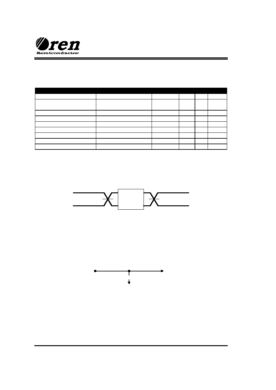
INPUT
1.5V
Device
under
test
OUTPUT
1.5V
Figure 5: AC Test I/O
Note:
During AC testing, inputs are driven to 0.45V and 2.4V levels. Unless otherwise specified, switching
times are measured from the 1.5V transition at the input, to the 1.5V transition at the output.
| |
C
L
25pF
Test
Point
Device
under
test
Figure 6: Normal AC Test Load

OR43300 DATA SHEET
Rev 2.1
December 10, 2001
Page 16
Company Confidential
www.oren.com
TCP
TCH
TCL
TIS
TIH
TCF
TCR
CLK_IN
SYNCHRO NO US
INPUTS
TOH
TOD
SYNCHRO NO US
O UTPUTS
Figure 7: CLK_IN and I/O Timing
CLK_IN
RESET #
DOUT &
SDAA#
TCRH
TCRS
IN TERN AL CLK VALID
OUTPUT
VALID
Figure 8: RESET# Timing
CLKIN
TOD
TEH
ADD
DIN
TIS
TIH
Figure 9: External EPROM Access Timing

OR43300 DATA SHEET
Rev 2.1
December 10, 2001
Page 17
Company Confidential
www.oren.com
TCH
TCD
ANALOG BASEBAND
VIDEO INPUT
CLMPGT
Figure 10: External Clamp Gate Timing
TNCOF
TNCOR
TNCOP
NCO_IN
TC F
TC R
CLK_IN
TCH
TCL
TCP
Figure 11: NCO_IN and CLK_IN Timing
SDA
SCL
TSTHD
THIGH
TR
TLOW
TF
TDSU
TDHD
TSP
TSTSU
TSTHD
TSPSU
TSPF
Figure 12: I
2
C Timing

OR43300 DATA SHEET
Rev 2.1
December 10, 2001
Page 18
Company Confidential
www.oren.com
5. MECHANICAL DIMENSIONS
80-pin Metric Quad Flat Package (MQFP)
14.0 0.10
(0.551 0.004)
14.0 0.10
(0.551 0.004)
0.8
0
B
S
C
(0
.
0
3
2
)
17.2 0.25
(0.677 0.10)
1.00 REF
(0.039)
20
.
0
0
.
1
0
(
0
.
7
8
7
0.004
)
20
.
0
0
.
1
0
(
0
.
7
8
7
0.004
)
23.
2
0
.
25
(
0
.
9
13
0.010)
0.3
5
0.05
(
0
.
0
14
0.002
)
SEATING
PLANE
0.076 (0.003)
0.33 (0.13)
0.70 TYP
(0.028)
1.60 REF
(0.063)
3.
40
M
a
x
(0
.
1
3
4
)
0.16 TYP
(.006)
0~7

OR43300 DATA SHEET
Rev 2.1
December
10,
2001
19
Company Confidential
www.oren.com
SALES OFFICES
OREN Semiconductor
2700 Augustine Drive, Suite 155
Santa Clara, California
USA 95054
tel: +1 408 330 0300
fax: +1 408 330 0305
OREN Semiconductor Ltd
P O Box 201
Yoqne'am Illit
ISRAEL 20692
tel: +972 4 909 5555
fax: +972 4 989 4566
OREN Semiconductor Japan
CO Kanematsu Corporation
2-1,Shibaura 1-Chome
Minato-Ku
Tokyo, Japan 105-8005
Tel: +81 3 5440 8621
Fax: +81 3 5440 6523