 | –≠–ª–µ–∫—Ç—Ä–æ–Ω–Ω—ã–π –∫–æ–º–ø–æ–Ω–µ–Ω—Ç: OX16CF950 | –°–∫–∞—á–∞—Ç—å:  PDF PDF  ZIP ZIP |

Oxford Semiconductor Ltd.
25 Milton Park, Abingdon, Oxon, OX14 4SH, UK
Tel: +44 (0)1235 824900
©
©
Oxford Semiconductor 2001 .
DATA SHEET .
CONFIDENTIAL .
F
EATURES
∑
Single full-duplex asynchronous channel
∑
128-byte deep transmitter / receiver FIFO
∑
Fully software compatible with industry standard
16C550 type UARTs
∑
Readable FIFO levels
∑
System clock up to 60MHz at 5V, 50 MHz at 3.3V
∑
Flexible clock prescaler from 1 to 31.875
∑
9-bit data framing as well as 5,6,7 and 8
∑
Detection of bad data in the receiver FIFO
∑
Automated in-band flow control using programmable
Xon/Xoff characters
∑
Transmitter and receiver can be disabled
∑
Low power CMOS
∑
3.3V / 5V operation
∑
Programmable by external Microwire
TM
EEPROM
(EEPROM programmed via Oxford Semiconductor
utilities).
∑
Extremely low power consumption by use of
asynchronous UART core and power down (sleep)
modes
∑
Ultra small 48 pin TQFP package.
∑
Supports all UART types 450 up to 950 (fully
programmable)
∑
CF+ Compliant (Revision 1.4).
∑
16-bit PC Card Compliant (PCMCIA Revision 7.1)
∑
8 bit Local Bus interface included for PCMCIA
applications
∑
2 Multi-purpose I/O pins which can be configured as
interrupt inputs
D
ESCRIPTION
The OXCF950 is a low cost asynchronous 16-bit PC card
(henceforth referred to as PCMCIA) or Compact Flash
(henceforth referred to as CF) UART (and Local Bus)
device. Local Bus Selection is performed by use of a
MODE pin. Note that Local Bus mode uses indirect
addressing, which is only supported by PCMCIA.
The 3.3V / 5V technology has been selected to allow the
device to be used in both high and low voltage
environments, as stated in the PCMCIA specification. Note
that when the OXCF950 is operating at 3.3V, its I/O is not
5V tolerant.
The EEPROM interface allows the programming of the
Attribute Memory, UART and Local Configuration Registers
during power up or hard/soft reset. This allows different
card manufacturers to modify the information contained in
the Attribute memory or UART/registers as required, for
example PC-Card ID value.
A number of power-down modes are included to keep
power consumption to a minimum. Such features include
clock division (fully programmable) and sleep modes when
a function of the OXCF950 is not being used.
The OXCF950 contains a single-channel ultra-high
performance UART offering data rates up to 15Mbps (at
5V) and 128-deep transmitter and receiver FIFOs. Deep
FIFOs reduce CPU overhead and allow utilisation of higher
data rates.
It is software compatible with the widely used industry-
standard 16C550 type devices and compatibles, as well as
other OX16C95x family devices.
In addition to increased performance and FIFO size, the
OXCF950 also provides enhanced features including
improved flow control. Automated software flow control
using Xon/Xoff and automated hardware flow control using
CTS#/RTS# and DSR#/DTR# prevent FIFO over-run. Flow
control and interrupt thresholds are fully programmable and
readable, enabling programmers to fine-tune the
performance of their system. FIFO levels are readable to
facilitate fast driver applications.
The addition of software reset enables recovery from
unforeseen error conditions allowing drivers to restart
gracefully. The OXCF950 supports 9-bit data frames used
in multi-drop industrial protocols. It also offers multiple
external clock options for isochronous applications, e.g.
ISDN, xDSL.
The OXCF950 also incorporates a bridge to an 8 bit Local
Bus in Local Bus Mode. It allows card developers to
expand the capabilities of their products by adding
peripherals to this bus. In addition, two user IO pins are
included to enhance external device control. These IO pins
can also be configured as interrupt inputs.
OXCF950
DATA SHEET

Page 2
OXCF950 DATA SHEET V1.1
OXFORD SEMICONDUCTOR LTD.
C
ONTENTS
FEATURES.....................................................................................................................................................................................1
DESCRIPTION...............................................................................................................................................................................1
CONTENTS.....................................................................................................................................................................................2
1 BLOCK DIAGRAM..............................................................................................................................................................5
2 PIN INFORMATION............................................................................................................................................................ 6
3 PIN DESCRIPTIONS ..........................................................................................................................................................6
4 CONFIGURATION & OPERATION...............................................................................................................................9
5 PCMCIA / CF TARGET CONTROLLER....................................................................................................................10
5.1
OPERATION........................................................................................................................................................................ 10
5.2
CONFIGURATION SPACE (CARD INFORMATION STRUCTURE) ................................................................................. 10
5.2.1
LOCAL BUS MODE SPACE MAP .................................................................................................................................. 10
5.2.2
NORMAL MODE SPACE MAP....................................................................................................................................... 11
5.3
ACCESS TO IO FUNCTION ............................................................................................................................................... 11
5.3.1
ACCESS TO INTERNAL UART...................................................................................................................................... 11
5.3.2
ACCESS TO LOCAL BUS .............................................................................................................................................. 11
5.3.3
ACCESSING LOCAL CONFIGURATION REGISTERS ................................................................................................. 12
5.4
CF / PCMCIA INTERRUPT................................................................................................................................................. 14
5.4.1
INTERRUPT GENERATION ........................................................................................................................................... 14
5.4.2
INTERRUPT SOURCES................................................................................................................................................. 15
5.5
CF/PCMCIA FUNCTION CONFIGURATION REGISTERS ............................................................................................... 15
5.5.1
CONFIGURATION OPTIONS REGISTER `COR' (OF FSET 0XF8) ............................................................................... 16
5.5.2
CONFIGURATION STATUS REGISTER `C SR' (OFFSET 0XFA) ................................................................................. 16
5.5.3
PIN REPLACEMENT REGISTER `PRR' (OFFSET 0 XFC) ............................................................................................ 17
5.5.4
SOCKET AND COPY REGISTER `SCR' (OFFSET 0XFE) ............................................................................................ 18
5.6
CARD INFORMATION STRUCTURE................................................................................................................................. 19
5.6.1
LOCAL BUS MODE......................................................................................................................................................... 19
5.6.2
NORMAL MODE............................................................................................................................................................. 20
6 INTERNAL 950 UART......................................................................................................................................................23
6.1
MODE SELECTION............................................................................................................................................................. 23
6.1.1
450 MODE....................................................................................................................................................................... 23
6.1.2
550 MODE....................................................................................................................................................................... 23
6.1.3
750 MODE....................................................................................................................................................................... 23
6.1.4
650 MODE....................................................................................................................................................................... 23
6.1.5
950 MODE....................................................................................................................................................................... 23
6.2
REGISTER DESCRIPTION TABLES ................................................................................................................................. 25
6.3
RESET CONFIGURATION ................................................................................................................................................. 28
6.3.1
HOST RESET .................................................................................................................................................................. 28
6.3.2
SOFTWARE RESET ....................................................................................................................................................... 28
6.4
TRANSMITTER & RECEIVER FIFOS................................................................................................................................ 28
6.4.1
FIFO CONTROL REGISTER `FCR'................................................................................................................................ 29
6.5
LINE CONTROL & STATUS............................................................................................................................................... 30
6.5.1
FALSE START BIT DETECTION .................................................................................................................................... 30
6.5.2
LINE CONTROL REGISTER `LCR'................................................................................................................................ 30
6.5.3
LINE STATUS REGISTER `LSR'.................................................................................................................................... 30
6.6
INTERRUPTS & SLEEP MODE ......................................................................................................................................... 32
6.6.1
INTERRUPT ENABLE REGISTER `IER' ........................................................................................................................ 32
6.6.2
INTERRUPT STATUS REGISTER `ISR' ........................................................................................................................ 33

Page 3
OXCF950 DATA SHEET V1.1
OXFORD SEMICONDUCTOR LTD.
6.6.3
INTERRUPT DESCRIPTION .......................................................................................................................................... 33
6.6.4
SLEEP MODE ................................................................................................................................................................. 34
6.7
MODEM INTERFACE......................................................................................................................................................... 34
6.7.1
MODEM CONTROL REGISTER `MCR'.......................................................................................................................... 34
6.7.2
MODEM STATUS REGISTER `MSR'............................................................................................................................. 35
6.8
OTHER STANDARD REGISTERS ..................................................................................................................................... 35
6.8.1
DIVISOR LATCH REGISTERS `DLL & DLM' ................................................................................................................. 35
6.8.2
SCRATCH PAD REGISTER `SPR'................................................................................................................................. 35
6.9
AUTOMATIC FLOW CONTROL......................................................................................................................................... 35
6.9.1
ENHANCED FEATURES REGISTER `EFR'................................................................................................................... 35
6.9.2
SPECIAL CHARACTER DETECTION............................................................................................................................ 37
6.9.3
AUTOMATIC IN-BAND FLOW CONTROL ..................................................................................................................... 37
6.9.4
AUTOMATIC OUT-OF-BAND FLOW CONTROL........................................................................................................... 37
6.10
BAUD RATE GENERATION............................................................................................................................................... 37
6.10.1
GENERAL OPERATION ................................................................................................................................................. 37
6.10.2
CLOCK PRESCALER REGISTER `CPR' ....................................................................................................................... 38
6.10.3
TIMES CLOCK REGISTER `TCR'................................................................................................................................... 38
6.10.4
INPUT CLOCK OPTIONS ............................................................................................................................................... 39
6.10.5
TTL CLOCK MODULE .................................................................................................................................................... 40
6.10.6
EXTERNAL 1X CLOCK MODE....................................................................................................................................... 40
6.10.7
CRYSTAL OSCILLATOR CIRCUIT ................................................................................................................................ 40
6.11
ADDITIONAL FEATURES .................................................................................................................................................. 40
6.11.1
ADDITIONAL STATUS REGISTER `ASR'...................................................................................................................... 40
6.11.2
FIFO FILL LEVELS `TFL & RFL'..................................................................................................................................... 41
6.11.3
ADDITIONAL CONTROL REGISTER `ACR'.................................................................................................................. 41
6.11.4
TRANSMITTER TRIGGER LEVEL `TTL' ........................................................................................................................ 42
6.11.5
RECEIVER INTERRUPT. TRIGGER LEVEL `RTL' ........................................................................................................ 42
6.11.6
FLOW CONTROL LEVELS `FCL & FCH' ....................................................................................................................... 42
6.11.7
DEVICE IDENTIFICATION REGISTERS ....................................................................................................................... 43
6.11.8
CLOCK SELECT REGISTER `CKS' ............................................................................................................................... 43
6.11.9
NINE-BIT MODE REGISTER `NMR'............................................................................................................................... 43
6.11.10
MODEM DISABLE MASK `MDM' .................................................................................................................................... 44
6.11.11
READABLE FCR `RFC'................................................................................................................................................... 45
6.11.12
GOOD-DATA STATUS REGISTER `GDS' ..................................................................................................................... 45
6.11.13
DMA STATUS REGISTER `DMS'................................................................................................................................... 45
6.11.14
PORT INDEX REGISTER `PIX'....................................................................................................................................... 45
6.11.15
CLOCK ALTERATION REGISTER `CKA'....................................................................................................................... 45
6.11.16
MISC DATA REGISTER ................................................................................................................................................. 45
7 SERIAL EEPROM SPECIFICATION..........................................................................................................................46
7.1
EEPROM DATA ORGANISATION ..................................................................................................................................... 46
7.2
ZONE 0 : HEADER.............................................................................................................................................................. 46
7.3
ZONE1 : CARD INFORMATION STRUCTURE ................................................................................................................. 47
7.4
ZONE 2 : LOCAL REGISTER CONFIGURATION............................................................................................................. 47
7.5
ZONE 3 : FUNCTION AC CESS (UART) ............................................................................................................................ 48
8 OPERATING CONDITIONS...........................................................................................................................................49
9 DC ELECTRICAL CHARACTERISTICS...................................................................................................................50
9.1
5V OPERATION .................................................................................................................................................................. 50
9.2
3V OPERATION .................................................................................................................................................................. 51
10 TIMING WAVEFORMS / AC CHARACTERISTICS...........................................................................................52
10.1
COMMON MEMORY ACCESS........................................................................................................................................... 52
10.2
ATTRIBUTE MEMORY ACCESS....................................................................................................................................... 53
10.3
I/O ACCESS........................................................................................................................................................................ 54
10.4
LOCAL BUS ACCESS........................................................................................................................................................ 55

Page 4
OXCF950 DATA SHEET V1.1
OXFORD SEMICONDUCTOR LTD.
11 PACKAGE INFORMATION .......................................................................................................................................57
12 ORDERING INFORMATION......................................................................................................................................58
NOTES............................................................................................................................................................................................59
CONTACT DETAILS .................................................................................................................................................................60
DISCLAIMER...............................................................................................................................................................................60

Page 5
OXCF950 DATA SHEET V1.1
OXFORD SEMICONDUCTOR LTD.
1 B
LOCK
D
IAGRAM
A[3:0]
1
D[7:0]
CE[1]#
OE#
WE#
IREQ#
IORD#
IOWR#
RESET
IOIS16#
REG#
PC Card
Interface
and Control
XTLI
XTLO
Clock &
Baudrate
Generator
EE_DO
EE_DI
EE_CK
EE_CS
EEPROM
Interface
Interrupt
Logic
Internal Data/Control Bus
SOUT
SIN
RTS#
DTR#
CTS#
DSR#
DCD#
RI#
UART
CIS and
configuratio
n registers
MIO pins
MIO[1:0]
Local Bus
LB_CS#
LB_WR#
LB_RD#
LB_RST
(Local Bus Mode Only
1
)
Config
Interface
MODE
Figure 1: Block Diagram
Page 6
OXCF950 DATA SHEET V1.1
OXFORD SEMICONDUCTOR LTD.
2 P
IN
I
NFORMATION
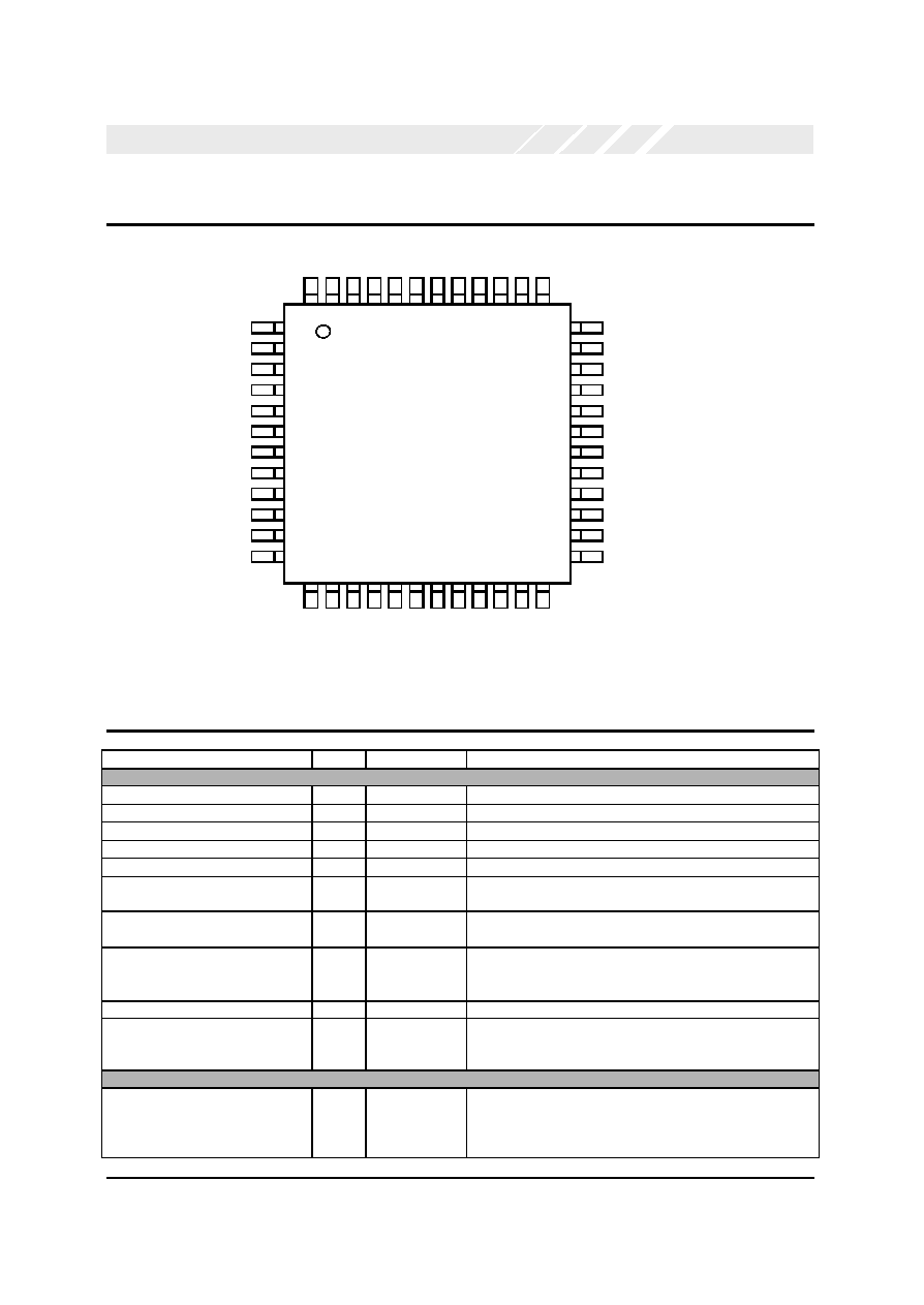
Figure 2: Pin Information
3 P
IN
D
ESCRIPTIONS
Pin Number
Dir
1
Name
Description
CF/PCMCIA Interface and Control
46, 45, 43, 42
I
A[3:0]
PCMCIA/CF address bus, bits [3:0]
6, 7, 10, 11, 12, 37, 38, 41
I/O
D[7:0]
PCMCIA/CF data bi-directional bus.
44
IU
REG#
Register select and I/O enable
5
IU
CE[1]#
Active low card enable
4
I
OE#
Active low memory read enable
1
I
WE#
Active-low write enable used for strobing Memory Write data
(Attribute memory).
3
IU
IORD#
Active-low I/O read enable
2
IU
IOWR#
Active-low I/O write enable
32
O
O
WP
IOIS16#
Write protect (in Memory only mode)
Data is 16 bit (in IO and Memory mode)
47
IU
RESET
PCMCIA/CF Reset
48
O
READY#
IREQ#
Device ready (in Memory only mode)
Active-low Interrupt request (in IO and Memory mode).
UART / Local Bus Function
24
O
SOUT
IrDA_Out
UART serial data output.
UART IrDA data output when MCR[6] is set in enhanced
mode.
OX16CF950
IREQ#
RESET
A3
A2
REG#
A1
A0
D0
PWR
GND
D1
D2
Local Bus
Normal
48
47
46
45
44
43
42
41
40
39
38
37
Mode
Mode
WE#
1
36
LB_WR#
/ A7
IOWR#
2
35
LB_RD#
/ A6
IORD#
3
34
LB_CS#
/ A5
OE#
4
33
LB_RST
/ A4
CE1#
5
32
IOIS16#
D7
6
31
MIO0
D6
7
30
RI#
GND
8
29
DCD#
PWR
9
28
DSR#
D5
10
27
CTS#
D4
11
26
DTR#
D3
12
25
RTS#
13
14
15
16
17
18
19
20
21
22
23
24
EE_CK
EE_CS
EE_DO
EE_DI
MODE
MIO1
GND
XTLI
XTLO
PWR
SIN
SOUT

Page 7
OXCF950 DATA SHEET V1.1
OXFORD SEMICONDUCTOR LTD.
23
I
SIN
IrDA_In
UART serial data input.
UART IrDA data input when IrDA mode is enabled (see
above).
29
I
DCD#
Active-low modem data-carrier-detect input.
26
O
DTR#
485_En
Tx_Clk_Out
Active-low modem data-terminal-ready output. If automated
DTR# flow control is enabled, the DTR# pin is asserted and
de-asserted if the receiver FIFO reaches or falls below the
programmed thresholds, respectively.
In RS485 half-duplex mode, the DTR# pin may be
programmed to reflect the state of the transmitter empty bit to
automatically control the direction of the RS485 transceiver
buffer (see register ACR[4:3]).
Transmitter 1x clock (baud rate generator output). For
isochronous applications, the 1x (or Nx) transmitter clock may
be asserted on the DTR# pin (see register CKS[5:4]).
25
O
RTS#
Active≠low modem request-to-send output. If automated
RTS# flow control is enabled, the RTS# pin is de-asserted
and reasserted whenever the receiver FIFO reaches or falls
below the programmed thresholds, respectively.
27
I
CTS#
Active-low modem clear-to-send input. If automated CTS#
flow control is enabled, upon de-assertion of the CTS# pin,
the transmitter will complete the current character and enter
the idle mode until the CTS# pin is reasserted. Note: flow
control characters are transmitted regardless of the state of
the CTS# pin.
28
I
DSR#
Rx_Clk_In
Active-low modem data-set-ready input. If automated DSR#
flow control is enabled, upon de-assertion of the DSR# pin,
the transmitter will complete the current character and enter
the idle mode until the DSR# pin is reasserted. Note: flow
control characters are transmitted regardless of the state of
the DSR# pin
External receiver clock for isochronous applications. The
Rx_Clk_In is selected when register CKS[1:0] = '01'
30
I
RI#
Tx_Clk_In
Active-low modem Ring-indicator input
External transmitter clock. This clock can be used by the
transmitter (and indirectly by the receiver) when register
CKS[6] = `1'.
21
O
XTLO
Crystal oscillator output
20
I
XTLI
Crystal oscillator input or external clock pin. Frequency
1.8MHz -> 60MHz
34
O
I
LBCS#
A[5]
Local Bus Mode : Active low local bus Chip select
Normal Mode : Address bit 5
35
O
I
LBRD#
2
A[6]
Local Bus Mode : Active-low local bus read enable
Normal Mode : Address bit 6
36
O
I
LBWR
A[7]
Local Bus Mode : Active-low local bus write enable
Normal Mode : Address bit 7
33
O
LBRST
2
A[4]
Local Bus Mode : Active high local bus Reset

Page 8
OXCF950 DATA SHEET V1.1
OXFORD SEMICONDUCTOR LTD.
I
Normal Mode : Address bit 4
EEPROM
13
O
EE_CK
EEPROM clock.
14
O
EE_CS
EEPROM active-high Chip Select.
16
I
EE_DI
EEPROM data in. This pin should be pulled up using 1-10k
resistor.
15
O
EE_DO
EEPROM data out.
Miscellaneous Pins
18, 31
I/O
MIO[1:0]
User defined IO pins.
Note: that if enabled, MIO[1:0] can be used as an interrupt
inputs.
17
I
MODE
Local Bus mode select. Note Local Bus mode requires
indirect addressing, which is only supported by the PCMCIA
specification
`0' = Normal Mode (CF/PCMCIA compatible)
`1' = Local Bus Mode (PCMCIA compatible)
Power and Ground
2
39, 19, 8
G
GND
Ground (0 Volts). The GND pins should be tied to ground
40, 22, 9
V
VDD
Power supply. The VDD pins should be tied to 5 Volts or 3.3
Volts
Table 1: Pin Descriptions
Note 1: Direction key:
I
Input
IU
Input with internal pull-up
ID
Input with external pull-down
O
Output
I/O
Bi-directional
G
Ground
V
3.3V/5V power

Page 9
OXCF950 DATA SHEET V1.1
OXFORD SEMICONDUCTOR LTD.
4
C
ONFIGURATION
& O
PERATION
PCMCIA and CF host systems allow for hot insertion of
cards.
Once a card has been inserted into a host system, the host
system will configure it. The PCMCIA standard defines two
card detect pins, that allow the host to be notified when a
card is inserted or removed.
By default the device will power up in either Normal or
Local Bus mode, depending on the mode pin. The
difference between these two modes is given in the
following table. Note that the Local Bus mode is not
suitable for CF systems.
Normal Mode (MODE=0)
Local Bus Mode (MODE=1)
Address bus is 8 bits wide. Address bus is 4 bits wide.
Indirect access is not used. Indirect access is used.
No external local bus.
External local bus supported.
Table 2: Differences between Normal & Local Bus Mode
The host system will wait for the READY# signal to be
active before reading the Card Information Structure, given
in attribute memory within the device. By reading this tuple
information, the host system is able to identify the device
type and the necessary resources requested by the device.
The host system will then load the device-driver software
according to this information and will configure the IO,
memory and interrupt resources. After determining that the
device is a memory and IO type device the host will enable
it's IO mode by writing to the device's Configuration
Options Register in attribute memory space. Device
drivers can then access the functions at the assigned
addresses.
A set of local configuration registers have been provided
that can be used to control the device's characteristics
(such as interrupt handling) and report internal functional
status. These registers can be accessed in IO space,
utilising the same IO space as the local bus (Local Bus
mode only) and are situated above the UART registers.
These local registers can be set up by device drivers or
from the optional EEPROM.
The EEPROM can also be used to redefine the reset
values of all register areas to tailor the device to the end
users requirements if the default values do not meet the
specific requirements of the manufacturer. This re-
programming of the device can also be performed for the
CIS area, allowing the manufacturer to mo dify resources
required, or Manufacturer ID values for example. As an
additional enhancement, the EEPROM can be used to pre-
program the UART, allowing pre-configuration, without
requiring device driver changes. This allows the enhanced
features of the integrated UART to be in place prior to
handover to any generic device drivers.
Note that a default set of tuples is provided for both
operating modes thus allowing for a single chip solution in
either mode.

Page 10
OXCF950 DATA SHEET V1.1
OXFORD SEMICONDUCTOR LTD.
5 PCMCIA / CF T
ARGET
C
ONTROLLER
5.1 Operation
Note: See section 10 for timing waveforms.
The OXCF950 responds to a number of different
CF/PCMCIA accesses (detailed below). Section 11
contains timing diagrams and information for each of these
types of access.
∑
Direct Common Memory read/writes
: These are
required in Local Bus mode only to allow indirect
access to attribute memory. This type of access is
permitted before and after configuration to allow the
reading of the CIS information, but is only supported
by the PCMCIA specification. Only 8 bit data, even
byte accesses are performed to this memory as it is
only used for access to the indirect attribute memory.
If the host attempts to access an invalid address, the
value of 0xFF (null) is returned.
∑
Direct Attribute Memory read/writes
: Access to direct
attribute memory is required in both CF and PCMCIA
specifications. This memory space contains all the
configuration information for the device, as well as the
configuration registers. In CF systems, where only
direct access is permitted, this space is the only
memory space that is accessed by the host system. If
the host attempts to access common memory in this
mode, the device will return 0xFF telling the host that
there is no valid data in this space. In Local Bus
Mode, the direct attribute memory informs the host
that indirect access is enabled allowing the host to
perform indirect access to attribute memory, via
common memory. Valid data is 8 bits wide and on
even bytes only, for direct attribute memory (as
defined in the PCMCIA 7.1 standard)
∑
Indirect Attribute Memory read/writes
(Local Bus mode
only): Access to indirect attribute memory is
performed through direct common memory. This
allows the device to provide full functionality with only
4 address pins. This access is performed to read the
CIS and also read/write to configuration registers.
Valid data is 8 bit wide and on even bytes only, for
indirect attribute memory (as defined in the PCMCIA
7.1 standard).
∑
IO read/writes
: IO accesses are performed to access
the UART, local bus (Local Bus mode) and local
configuration registers. Data width is restricted to 8
bits, as required by the standard UART function. As
the device CIS information configures the card as a
single function device, no base addresses need to be
defined thus simplifying access to the function. As
reads and writes are immediate, there is no
requirement to hold the WAIT# signal in its active
state, thus providing maximum speed access to IO
space.
5.2 Configuration Space (Card Information
Structure)
5.2.1 Local Bus Mode Space Map
Direct
Indirect
Main CIS either:
a) Normal Default
b) Bluetooth Default
c) Custom CIS
(downloaded from
EEPROM)
0xFF
Common
(Valid at even
locations only)
0x00
0x00
0x00
0xFF
0xFF
0x00
0xFF
Indirect Access
Register
Hard Coded CIS to
link to indirect space
0x0F
0x10
0x0F
0x10
0x7F
0x80
Attribute
Function
Configuration
Registers
0xF6
0xF8
NOT VALID
NOT VALID
NOT VALID
Figure 3: Local Bus mode memory space map

Page 11
OXCF950 DATA SHEET V1.1
OXFORD SEMICONDUCTOR LTD.
Figure 4: Normal Mode memory space map
5.2.2 Normal Mode Space Map
5.3 Access to IO Function
5.3.1 Access to Internal UART
Access to the internal UART is achieved via standard IO
mapping. As the device is configured as a single function
device, no base address is required to access the UART.
As IO mapping is used, access to the UART is permitted
only after the card has been configured. Once the
Configuration Options Register has been set in the
Attribute area, the UART can be accessed following the
mapping shown in Table 3.
UART Address (hex)
CF/PCMCIA offset from
address 0 for UART
function in IO space (hex)
0
0
1
1
2
2
3
3
4
4
5
5
6
6
7
7
Table 3: UART's mapping in I/O space
5.3.2 Access to Local Bus
Access to the internal Local Bus is achieved via standard
IO mapping. The Local Bus function is available in Local
Bus mode only as it's device pins are used as the extended
address bits required for direct access in Normal mode.
Indirect access is only supported in the PCMCIA
specification, so the local bus is only available in PCMCIA
systems. As the device is configured as a single function
device, no base address is required to access the Local
Bus. As IO mapping is used, access to the Local Bus is
permitted only after the card has been configured. Once
the Configuration Options Register has been set in the
Attribute area, the Local Bus can be accessed following the
mapping shown in table Table 4. This access is permitted
only if bit[0] is reset to `0' in the MDR register in the UART,
otherwise the local configuration registers will be accessed
rather than the local bus.
Local Bus Address
1
(hex) CF/PCMCIA offset from
address 0 for Local Bus
function in IO space (hex)
0
8
1
9
2
A
3
B
4
C
5
D
6
E
7
F
Table 4: Local Bus mapping in I/O space
Note 1: Although only 4 bits of IO address space are
requested by the default CIS in the device, the address
range may be extended past these four bits. This can be
achieved by modifying the CIS, via the EEPROM, and
connecting the extended address bits to the external local
bus device.
Direct
Indirect
Main CIS either:
a) Normal Default
b) Bluetooth Default
c) Custom CIS
(downloaded from
EEPROM)
0xFF
Common
(Valid at even
locations only)
0x00
0x00
0x00
0xFF
0xFF
0x00
0xFF
Attribute
Additional Storage
Space, which can be
downloaded from the
EEPROM.
0x7F
0x80
Function
Configuration
Registers
0xF8
0xF6
NOT VALID
NOT VALID
NOT VALID

Page 12
OXCF950 DATA SHEET V1.1
OXFORD SEMICONDUCTOR LTD.
5.3.3 Accessing Local Configuration Registers
The local configuration registers are a set of device specific registers, which can be accessed via standard IO mapping. As the
device is configured as a single function device, no base address is required to access the local configuration registers. Since IO
mapping is used, access to the local configuration registers is permitted only after the card has been configured. Once the
Configuration Options Register has been set in the Attribute area, the local configuration registers can be accessed following the
mapping shown in Table 5. This access is always permitted in Normal Mode. In Local Bus Mode access is only permitted if bit[0]
is set to `1' in the MDR register in the UART, otherwise the local bus will be accessed rather than the local configuration
registers.
CF/PCMCIA offset from address 0 for local
configuration registers in IO space (hex)
Register Map
8
EEPROM Status and Control register
9
Multi-Purpose I/O Configuration register
A
UART Divider/Interrupt Pulse Width Divider register
B
Mode Status register
C
Interrupt Status register
D
Soft UART/Local Bus reset register
E
Reserved
F
Reserved
Table 5: Local Configuration Register's mapping in I/O space
Each of the local configuration registers are explained in the following sections
EEPROM Status and Control register `ESC'(Offset 0x08)
This register defines the control on the serial EEPROM. The individual bits are described in Table 6.
Read/Write
Bits
Description
EEPROM PCMCIA
Reset
7:5
Reserved
-
R
000
4
EEPROM Data In.
For reads from the EEPROM this input bit is the output-data (DO) of the
external EEPROM connected to EE_DI pin
-
R
X
3
EEPROM Data Out.
For writes to the EEPROM, this output bit feeds the input-data of the
external EEPROM (DI). This bit is output on the devices EE_DO and
clocked into the EEPROM by EE_CK
-
R/W
0
2
EEPROM Clock.
For reads or writes to the external EEPROM toggle this bit to generate an
EEPROM clock (EE_CK pin)
-
R/W
0
1
EEPROM Chip Select.
When `1' the EEPROM chip select pin EE_CS is activated (high). When `0'
EE_CS is de-activated (low)
-
R/W
0
0
EEPROM Valid
A `1' indicates that a valid EEPROM program header is present
-
R
X
Table 6: EEPROM Status and Control Register

Page 13
OXCF950 DATA SHEET V1.1
OXFORD SEMICONDUCTOR LTD.
Multi-Purpose I/O Configuration register `MIC' (Offset 0x09)
This register configures the operation for the multi-purpose I/O pins `MIO[1:0]' as follows
Read/Write
Bits
Description
EEPROM PCMCIA
Reset
7:4
Reserved
-
R
0000
3:2
MIO1 Configuration register
00 -> MIO1 is a non-inverting input pin
01 -> MIO1 is an inverting input pin
10 -> MIO1 is an output pin driving `0'
11 -> MIO1 is an output pin driving `1'
W
R/W
00
1:0
MIO0 Configuration register
00 -> MIO0 is a non-inverting input pin
01 -> MIO0 is an inverting input pin
10 -> MIO0 is an output pin driving `0'
11 -> MIO0 is an output pin driving `1'
W
R/W
00
Table 7: Multi Purpose I/O Configuration Register
UART Divider/Interrupt Pulse Width Divider register `DIV' (Offset 0x0A)
This register defines the divide values (2^N division) for the clocks to the UART and Interrupt pulse generator signal. This allows
the device to be set up in its lowest power mode possible, and is fully programmable by the host or the EEPROM. The default
value for the UART clock divider provides a clock to the UART of x1. The default value for the Interrupt pulse divider provides a
clock to the interrupt processor of /32. See Section 5.4.1 Note that the UART clock rate should not be changed without then
resetting the UART(see SRT register).
Read/Write
Bits
Description
EEPROM PCMCIA
Reset
7:6
Reserved
-
R
00
5:3
Uart clock divide value.
The division ratio is 2^N, giving 1, 2, 4, 8, 16, 32, 64, 128
W
R/W
000
2:0
Interrupt Pulse divide value:
This field should be set under the following clock freq. conditions
000 -> when clock frequency is less than 2MHz
001 -> when clock frequency is between 2 and 4MHz
010 -> when clock frequency is between 4 and 8MHz
011 -> when clock frequency is between 8 and 16MHz
100 -> when clock frequency is between 16 and 32MHz
101 -> when clock frequency is between 32 and 64MHz
110 -> RESERVED
111 -> RESERVED
W
R/W
101
Table 8: UART Divider/ Interrupt Pulse Width Divider
Mode Status register `MSR' (Offset 0x0B)
This read only register return the state of the MODE pin (i.e. whether in Normal or Local Bus modes).
Read/Write
Bits
Description
EEPROM PCMCIA
Reset
7:1
Reserved
-
R
0000000
0
Mode
O = Normal, 1 = Local Bus
-
R
X
Table 9: Mode Status Register

Page 14
OXCF950 DATA SHEET V1.1
OXFORD SEMICONDUCTOR LTD.
Interrupt Status and Control register `ISR' (Offset 0x0C)
This register controls the assertion of interrupts from the User I/O pins (MIO[1:0]) as well as returning the internal status of the
interrupt sources.
Read/Write
Bits
Description
EEPROM PCMCIA
Reset
7:5
Reserved
-
R
000
4
UART Interrupt status
This bit reflects the state of the internal UART interrupt
-
R
0
3
MIO[1] interrupt mask
When set to `1' allows pin MIO[1] to assert an interrupt on the devices
IREQ# pin. The state of the MIO[1] signal that causes an interrupt is
dependent upon the polarity set by the register fields MIC[3:2].
W
R/W
0
2
MIO[0] interrupt mask
When set to `1' allows pin MIO[0] to assert an interrupt on the devices
IREQ# pin. The state of the MIO[0] signal that causes an interrupt is
dependent upon the polarity set by the register fields MIC[1:0].
W
R/W
0
1
MIO1 Internal state
This bit reflects the state of the internal MIO[1]. The internal MIO[1] signal
reflects the non-inverted or inverted state of MIO[1] pin
-
R
X
0
MIO0 Internal state
This bit reflects the state of the internal MIO[0]. The internal MIO[0] signal
reflects the non-inverted or inverted state of MIO[0] pin
-
R
X
Table 10: Interrupt Status Register
Soft UART/Local Bus reset register `SRT' (Offset 0x0D)
This register controls the soft reset passed to the UART and local bus reset. These reset lines are in addition to the soft reset
that may be produced by the host (bit[7] of the COR register in attribute memory space). Note that the local bus reset is used in
Local Bus mode only and not in Normal mode. Note these bits are not self-clearing.
Read/Write
Bits
Description
EEPROM PCMCIA
Reset
7:2
Reserved
-
R
000000
1
Active high soft reset for UART
W
R/W
0
0
Active high soft reset for Local Bus
W
R/W
0
Table 11: Soft UART / Local Bus Reset (LB reset used in Local Bus Mode only)
5.4 CF / PCMCIA Interrupt
5.4.1 Interrupt Generation
PCMCIA/CF cards support pulse or level type interrupt signals to request interrupt service from the host system. The CIS of the
card specifies whether pulse, level or both types of interrupt can be generated. Once the host has read the CIS it is able to set
the LevlReq field in the Configuration Options Register (COR) to tell the card which type of interrupts should be generated.
The OXCF950 is capable of generating either type of interrupt. However, to reduce power consumption, the default CIS states
that only level type interrupts can be generated. A custom CIS can be constructed that specifies the card has the ability to
generate pulse type interrupts, if this is required, by using an external EEPROM.
The OXCF950 uses a programmable clock divider circuit to generate pulse type interrupts signals. The pulse that is generated is
one clock cycle (after division) in length. The divider circuit can be programmed by setting the contents of the Interrupt Pulse

Page 15
OXCF950 DATA SHEET V1.1
OXFORD SEMICONDUCTOR LTD.
Divide Value field in the DIV local configuration register (see section 6.3.4.3). This allows the length of the pulse to be varied, so
that different clock frequencies can be used and the pulse can still be kept as short as possible, without violating the minimum
length of 50
µ
s as defined in the PCMCIA Standard. Table 12 shows how the register should be programmed for different clock
frequencies.
Clock Frequency (MHz)
Interrupt Divider Setting
f
<
2
000
2
<=
f
<
4
001
4
<=
f
<
8
010
8
<=
f
< 16
011
16 <=
f
< 32
100
32 <=
f
< 64
101
110
RESERVED
111
Table 12: Interrupt Pulse Divide Value settings
5.4.2 Interrupt Sources
The OXCF950 has three possible interrupt sources. These are the internal UART, and the two multi-purpose I/O pins, which can
be configured as interrupts using the MIO Configuration Register (MIC ≠ see section 6.3.4.2) and the Interrupt Status and Control
Register (ISR ≠ see section 6.3.4.5)
When the OXCF950 is requesting interrupt service, the Intr field within the Configuration Status Register (CSR ≠ see section
6.5.2) will be set to 1. Otherwise this field will be cleared to 0. The Intr field value is controlled by the interrupt source (i.e UART
or MIO [1:0]). The status of the actual interrupts can be read from the ISR register.
5.5 CF/PCMCIA Function Configuration Registers
Each PCMCIA/CF card's I/O function must implement Function Configuration Registers (FCR). These registers allow the host to
configure the function provided by the card, and are mapped into the attribute memory space at the location specified within the
CONFIG tuple (in the CIS). The CONFIG tuple defines a base address for the Function Configuration Registers and a number
corresponding to how may registers are supported (4 registers in the OXCF950). Each of these registers has read/write
capability and is mapped at even location, consistent with the design of attribute memory. The registers supported in the
OXCF950 are shown in the following table.
Offset from
FCR base
address
Attribute
memory address
Register
0
F8
Configuration Options Register
2
FA
Configuration and Status Register
4
FC
Pin Replacement Register
8
FE
Socket & Copy Register
Table 13: Configuration Register Mapping
Due to the type of function the OXCF950 configures the card to be, and the fact that it is a single function device, only a sub-set
of the total number of configuration registers are required.
The definition of each configuration register is detailed in the next few sub-sections.

Page 16
OXCF950 DATA SHEET V1.1
OXFORD SEMICONDUCTOR LTD.
5.5.1 Configuration Options Register `COR' (offset 0xF8)
The configuration options register is used to configure PCMCIA/CF cards that have programmable address decoders. Once the
card's client driver has successfully parsed the CIS, it will attempt to obtain system resources, as requested by the CIS. On
completion of this it assigns the resources to the card via the COR. The COR format and description is given in Table 14.
D7
D6
D5
D4
D3
D2
D1
D0
SRESET
LevIREQ
Function Configuration Index
Field
Type
Description
SRESET
R/W
Software reset
Setting this field to `1' places the card in the reset state. This is equivalent to
setting the RESET signal (on pin) except this SRESET field is not reset.
Returning this field to `0' leaves the card in the same un-configured, reset state
as the card would be following a power-up and hard reset.
LevIREQ
1
R/W
Level Mode IREQ#
Setting this field to `1' enables level type interrupts
Setting this field to `0' enables pulse type interrupts
Function Configuration Index
R/W
Configuration Index
The host sets this field to the value of the Configuration Entry Number field of a
Configuration Table Entry tuple as defined in the CIS. On setting the non-zero
value in this field the function IO is enabled and IO accesses are allowed. When
the field is set to zero (e.g. after a hard reset) the card will be configured to
memory only mode and all IO accesses will be ignored by the card.
Table 14: Configuration Option Register
Note 1
The default tuples in the CIS tell the host that only level type interrupts are supported to allow lowest power consumption. The
OXCF950 supports both level and pulse type interrupts, and if a particular manufacturer requires to use pulse type, or both, then
the CIS can be modified using the external EEPROM.
5.5.2 Configuration Status Register `CSR' (Offset 0xFA)
The Configuration and Status Register is an optional register, supported by the OXCF950. The register allows additional control
over a function's configuration and reports status related to the function's configuration.
D7
D6
D5
D4
D3
D2
D1
D0
Changed
SigChg
IOIs8
RFU
Audio
PwrDwn
Intr
IntrAck
Field
Type
Description
Changed
R
If a PCMCIA/CF card is using the I/O interface, the function's Pin Replacement
register is present and one or more of the state change signals in the Pin
Replacement Register are set to one(1), or one Event bits in the Extended Status
Register are set (1) and the corresponding Enable bit is set (1), the function shall
set this field to one (1).
If a PCMCIA/CF card is not using the I/O interface or the function's Pin
Replacement register is not present, this field is undefined and should be
ignored.
SigChg
1
R/W
This field serves as a gate for STSCHG#
If a PCMCIA/CF card is using the I/O interface and both the Changed and
SigChg fields are set to one (1), the function shall assert STSCHG#.

Page 17
OXCF950 DATA SHEET V1.1
OXFORD SEMICONDUCTOR LTD.
If a PCMCIA/CF card is using the I/O interface and this field is reset to zero (0),
the function shall not assert STSCHG#.
If a PCMCIA/CF card is not using the I/O interface or the function's Pin
Replacement register is not present, this field is undefined and should be
ignored.
IOIs8
R/W
The host sets this field to one (1) when it can provide I/O cycles only with an 8-bit
D[7..0] data path. The card is guaranteed that accesses to the 16-bit registers will
occur as two byte accesses rather than as a single 16-bit access.
RFU
-
Reserved. Must be zero (0).
Audio
2
R/W
This bit is set to one (1) to enable audio information on SPKR# when the card is
configured.
PwdDwn
3
R/W
When the host sets this field to one (1), the function shall enter a power-down
state, if such a state exists.
If a PCMCIA/CF card function does not have a power-down state, the function
shall ignore this field.
Intr
R
Interrupt Request / Acknowledge ≠ This field reports whether the function is
requesting interrupt servicing and may be used to acknowledge the host system
is ready to process another interrupt request from the PCMCIA/CF card.
The function shall set this field to one (1) when it is requesting interrupt service.
The function shall set this field to zero (0) when it is not requesting interrupt
service.
Writes to this field are ignored when the IntrAck field of all Configuration and
Status Registers on the PCMCIA/CF card are reset to zero (0).
IntrAck
R/W
Single function cards ignore this field on writes and always return zero (0).
Table 15: Configuration Status Register
Note 1
The STSCHG# signal is optional and is not supported on the OXCF950, to reduce the complexity of the device.
Note 2
Audio is not supported on the device.
Note 3
The OXCF950 does not support a specific power down mode, since it is a low power device that features a number of sleep
modes (see Section 7 for further details).
5.5.3 Pin Replacement Register `PRR' (Offset 0xFC)
The Pin Replacement Register is implemented to provide information about READY, WP or the BVD[2..1] status when
implementing the I/O interface.
D7
D6
D5
D4
D3
D2
D1
D0
CBVD1
CBVD2
CREADY
CWProt
RBVD1
RBVD2
RREADY
RWProt
Field
Description
CBVD1
This bit is set (1) when the corresponding bit, RBVD1, changes state. This bit may also be
written by the host.
CBVD2
This bit is set (1) when the corresponding bit, RBVD2, changes state. This bit may also be
written by the host.

Page 18
OXCF950 DATA SHEET V1.1
OXFORD SEMICONDUCTOR LTD.
written by the host.
CREADY
This bit is set (1) when the corresponding bit, RREADY, changes state. This bit may also be
written by the host.
CWProt
This bit is set (1) when the corresponding bit, RWProt, changes state. This bit may also be
written by the host.
RBVD1
When read, this bit represents the internal state of the Battery Voltage Detect circuits which
would be on the BVD1 pin.
When this bit is written as 1 the corresponding CBVD1 bit is also written. When this bit is
written as 0, the CBVD1 bit is unaffected.
RBVD2
When read, this bit represents the internal state of the Battery Voltage Detect circuits which
would be on the BVD2 pin.
When this bit is written as 1 the corresponding CBVD2 bit is also written. When this bit is
written as 0, the CBVD2 bit is unaffected.
RREADY
When read, this bit represents the internal state of the READY signal. This bit may also be
used to determine the state of READY as that pin has been relocated for use as Interrupt
Request on IO Cards.
When this bit is written as 1 the corresponding "changed" bit is also written. When this bit is
written as 0, the "changed" bit is unaffected.
RWProt
When read, this bit represents the state of the WP signal. This signal may also be used to
determine the state of the Write Protect switch when pin 33 is being used for IOIS16#.
When this bit is written as 1 the corresponding "changed" bit is also written. When this bit is
written as 0, the "changed" bit is unaffected.
Table 16: Pin Replacement Register
5.5.4 Socket and Copy Register `SCR' (Offset 0xFE)
This is an optional read/write register, implemented by the OXCF950, which the PCMCIA/CF card may use to distinguish
between similar cards installed in a system. This register is always written by the system before writing the card's Function
Configuration Index field in the Configuration Option register.
D7
D6
D5
D4
D3
D2
D1
D0
Reserved
Copy Number
Socket Number
Field
Description
Reserved
This bit is reserved for future standardization. This bit must be set to zero (0) by software when
the register is written.
Copy Number
PCMCIA/CF cards that indicate in their CIS that they support more than one copy of identically
configured cards, should have a copy number (0 to MAX twin cards, MAX = n-1) written back
to the socket and Copy register.
This field indicates to the card that it is the n'th copy of the card installed in the system, which
is identically configured. The first card installed receives the value 0. This permits identical
cards designed to share a common set of I/O ports while remaining uniquely identifiable and
consecutively ordered.
Socket Number
This field indicates to the PCMCIA/CF card that it is located in the n'th socket. The first socket
is numbered o. This permits any cards designed to do so to share a common set of I/O ports
while remaining uniquely identifiable.
Table 17: Socket and Copy Register

Page 19
OXCF950 DATA SHEET V1.1
OXFORD SEMICONDUCTOR LTD.
5.6 Card Information Structure
5.6.1 Local Bus Mode
Value
(Hex)
Tuple Name
Description
Direct Attribute
0x01
0x02
0x00
0xFF
CISTPL_DEVICE
CIS should start with a CISTPL_DEVICE tuple.
0x03
0x00
CISTPL_INDIRECT
Use indirect access register (located in direct common memory).
0xFF CISTPL_END
Indirect Attribute
0x13
0x03
0x43
0x49
0x53
CISTPL_LINKTARGET
The first tuple in indirect memory must be a CISTPL_LINKTARGET to prove that a
valid CIS chain is present. The host will start processing from location 0 of the
indirect attribute memory, after following an implied link from the primary CIS chain
in direct attribute memory.
0x1C
0x03
0x03
0x00
0xFF
CISTPL_DEVICE_OC
This tuple allows the device to be operated at 3.3 volts as well as at 5.0 volts.
0x20
0x04
0x79
0x02
0x0B
0x95
CISTPL_MANFID
This tuple specifies the manufacturer ID and product ID codes (0x0279 and 0x950B
respectively).
0x21
0x02
0x02
0x01
CISTPL_FUNCID
This tuple specifies the function of the device, in this case the tuple states the device
is a serial port.
0x22
0x04
0x00
0x02
0x0F
0x7F
CISTPL_FUNCE
This tuple is the function extension tuple, and provides more detailed information
about the function of the device, and provides the following information:
∑
Serial port includes a 16550 compatible UART.
∑
Space, Mark, Odd and Even parity
∑
5, 6, 7, 8 bit chars
∑
1, 1.5 and 2 stop bit operation.
0x15
0x15
0x07
0x01
0x50
0x43
0x20
0x43
0x41
0x52
0x44
0x00
CISTPL_VERS_1
The Level 1 version / product information tuple provides the host with the following
information:
∑
The device supports version 7.1 of the PC Card Specification.
∑
The Manufacturer String is "PC CARD"
∑
The Product String is "GENERIC"
∑
The Additional Product Information strings are empty.

Page 20
OXCF950 DATA SHEET V1.1
OXFORD SEMICONDUCTOR LTD.
0x47
0x45
0x4E
0x45
0x52
0x49
0x43
0x00
0x00
0x00
0xFF
0x1A
0x04
0x00
0x02
0xF8
0x0F
CISTPL_CONFIG
The CISTPL_CONFIG tuple provides basic configuration information including the
following:
∑
Base address of the configuration registers (specified as 0xFA)
∑
Which configuration registers are present and supported (Configuration
Options Register, Configuration Status Register, Pin Replacement
Register, and Socket and Copy Register are supported).
∑
Index of the last Configuration Table Entry (set to 0x02).
0x1B
0x0D
0xC1
0x41
0x99
0x01
0xB5
0x1E
0xA0
0x40
0x0F
0xB0
0xFF
0xFF
0x07
CISTPL_CFTABLE_ENTRY This tuple specifies one particular configuration that the device can be used in. Each
configuration has an index number, which is used by the host to select it. This
configuration has the following properties:
∑
Index is 0x01
∑
READY signal is active, and configuration is for I/O and Memory mode.
∑
Nominal Vcc is set to be 3.30 volts.
∑
Requests 16 bytes of I/O space.
∑
Level interrupts, interrupt sharing are supported.
∑
Any interrupt (IRQ0-15) can be used.
∑
Maximum number of identical cards is set to 8.
0x1B
0x04
0x02
0x01
0x01
0x55
CISTPL_CFTABLE_ENTRY This configuration is based on the previous configuration, except that it requests Vcc
to be 5.0 volts.
0xFF
CISTPL_END
End of CIS
Table 18: Card Information Structure Values (Local Bus Mode)
5.6.2 Normal Mode
Value
(Hex)
Tuple Name
Description
Direct Attribute
0x01
0x03
0x00
0x00
0xFF
CISTPL_DEVICE
CIS should start with a CISTPL_DEVICE tuple. (Allows operation at 5.0 volts)

Page 21
OXCF950 DATA SHEET V1.1
OXFORD SEMICONDUCTOR LTD.
0x1C
0x03
0x03
0x00
0xFF
CISTPL_DEVICE_OC
The CISTPL_DEVICE_OC tuple allows operation at 3.3 volts.
0x20
0x04
0x79
0x02
0x0B
0x95
CISTPL_MANFID
This tuple specifies the manufacturer ID and product ID codes (0x0279 and 0x950B
respectively).
0x21
0x02
0x02
0x01
CISTPL_FUNID
This tuple specifies the function of the device, in this case the tuple states the device
is a serial port.
0x22
0x04
0x00
0x02
0x0F
0x7F
CISTPL_FUNCE
This tuple is the function extension tuple, and provides more detailed information
about the function of the device, and provides the following information:
∑
Serial port includes a 16550 compatible UART.
∑
Space, Mark, Odd and Even parity
∑
5, 6, 7, 8 bit chars
∑
1, 1.5 and 2 stop bit operation.
0x15
0x15
0x07
0x01
0x43
0x46
0x20
0x43
0x41
0x52
0x44
0x00
0x47
0x45
0x4E
0x45
0x52
0x49
0x43
0x00
0x00
0x00
0xFF
CISTPL_VERS_1
The Level 1 version / product information tuple provides the host with the following
information:
∑
The device supports version 7.1 of the PC Card Specification.
∑
The Manufacturer String is "CF CARD"
∑
The Product String is "GENERIC"
The Additional Product Information strings are empty.
0x1A
0x04
0x00
0x04
0xF8
0x0F
CISTPL_CONFIG
The CISTPL_CONFIG tuple provides basic configuration information including the
following:
∑
Base address of the configuration registers (specified as 0xFA)
∑
Which configuration registers are present and supported (Configuration
Options Register, Configuration Status Register, Pin Replacement
Register, and Socket and Copy Register are supported).
∑
Index of the last Configuration Table Entry (set to 0x04).
0x1B
0x0F
CISTPL_CFTABLE_ENTRY This tuple specifies one particular configuration that the device can be used in. Each
configuration has an index number, which is used by the host to select it. This
configuration has the following properties:

Page 22
OXCF950 DATA SHEET V1.1
OXFORD SEMICONDUCTOR LTD.
0xC1
0x41
0x99
0x01
0xB5
0x1E
0xA8
0x60
0xF8
0x03
0x0F
0xB0
0xFF
0xFF
0x07
configuration has the following properties:
∑
Index is 0x01
∑
READY signal is active, and configuration is for I/O and Memory mode.
∑
Nominal Vcc is set to be 3.30 volts.
∑
Requests 16 bytes of I/O space, starting at 0x03F8.
∑
Level interrupts, interrupt sharing are supported.
∑
Any interrupt (IRQ0-15) can be used.
∑
Maximum number of identical cards is set to 8.
0x1B
0x03
0x02
0x08
0x2F
CISTPL_CFTABLE_ENTRY This configuration is based on the previous configuration, except that it specifies the
I/O space can start anywhere.
0x1B
0x0E
0xC3
0x41
0x99
0x01
0x55
0xA8
0x60
0xF8
0x03
0x0F
0xB0
0xFF
0xFF
0x07
CISTPL_CFTABLE_ENTRY This tuple specifies one particular configuration that the device can be used in. Each
configuration has an index number, which is used by the host to select it. This
configuration has the following properties:
∑
Index is 0x01
∑
READY signal is active, and configuration is for I/O and Memory mode.
∑
Nominal Vcc is set to be 5.0 volts.
∑
Requests 16 bytes of I/O space, starting at 0x03F8.
∑
Level interrupts, interrupt sharing are supported.
∑
Any interrupt (IRQ0-15) can be used.
∑
Maximum number of identical cards is set to 8.
0x1B
0x03
0x04
0x08
0x2F
CISTPL_CFTABLE_ENTRY This configuration is based on the previous configuration, except that it specifies the
I/O space can start anywhere.
0xFF
CISTPL_END
Table 19: Card Information Structure Values (Normal Mode)

Page 23
OXCF950 DATA SHEET V1.1
OXFORD SEMICONDUCTOR LTD.
6 I
NTERNAL
950 UART
The internal UART within the OXCF950 is based on the 16C950 rev B, and is henceforth referred to as the 950 core. Some
modes of the 16C950 rev B that are configured by pin options such as Extended-550 mode are not available in this embedded
core.
6.1 Mode Selection
The 950 core is software compatible with the 16C450, 16C550, 16C654 and 16C750 UARTs. The operation of the 950 depends
on a number of mode settings. These modes are referred to throughout this data sheet. The FIFO depth and compatibility modes
are tabulated below:
UART Mode
FIFO
size
FCR[0] Enhanced mode
(EFR[4]=1)
FCR[5]
(guarded with LCR[7] = 1)
450
1
0
X
X
550
16
1
0
0
650
128
1
1
X
750
128
1
0
1
950*
128
1
1
X
Table 20: UART Mode Configuration
* Note that 950 mode configuration is identical to 650 configuration
6.1.1 450 Mode
After a hardware reset bit 0 of the FIFO Control Register
(`FCR') is cleared, hence the 950 is compatible with the
16C450. The transmitter and receiver FIFOs (referred to as
the `Transmit Holding Register' and `Receiver Holding
Register' respectively) have a depth of one. This is referred
to as `Byte mode'. When FCR[0] is cleared, all other mode
selection parameters are ignored.
6.1.2 550 Mode
After a hardware reset, writing a 1 to FCR[0] will increase
the FIFO size to 16, providing compatibility with 16C550
devices.
6.1.3 750 Mode
Writing a 1 to FCR[0] will increase the FIFO size to 16. In a
similar fashion to 16C750, the FIFO size can be further
increased to 128 by writing a 1 to FCR[5]. Note that access
to FCR[5] is protected by LCR[7]. I.e., to set FCR[5],
software should first set LCR[7] to temporarily remove the
guard. Once FCR[5] is set, the software should clear
LCR[7] for normal operation.
The 16C750 additional features over the 16C550 are
available as long as the UART is not put into Enhanced
mode (i.e. EFR[4] should be `0'). These features are:
1. Deeper FIFOs
2. Automatic RTS/CTS out-of-band flow control
3. Sleep mode
6.1.4 650 Mode
The 950 is compatible with the 16C650 when EFR[4] is set,
i.e. the device is in Enhanced mode. As 650 software
drivers usually put the device into Enhanced mode, running
650 drivers on the 950 will result in 650 compatibility with
128 deep FIFOs, as long as FCR[0] is set. Note that the
650 emulation mode of the 950 provides 128 byte deep
FIFOs whereas the standard 16C650 has only 32 byte
FIFOs.
650 mode has the same enhancements as the 16C750
over the 16C550, but these are enabled using different
registers.
There are also additional enhancements over those of the
16C750 in this mode, these are:
1. Automatic in-band flow control
2. Special character detection
3. Infra-red "IrDA-format" transmit and receive mode
4. Transmit trigger levels
5. Optional clock prescaler
6.1.5 950 Mode
The additional features offered in 950 mode generally only
apply when the UART is in Enhanced mode (EFR[4]='1').
Provided FCR[0] is set, in Enhanced mode the FIFO size is
128.
Note that 950 mode configuration is identical to that of 650
mode, however additional 950 specific features are

Page 24
OXCF950 DATA SHEET V1.1
OXFORD SEMICONDUCTOR LTD.
enabled using the Additional Control Register `ACR' (see
section 6.11.3). In addition to larger FIFOs and higher baud
rates, the enhancements of the 950 over the 16C654 are:
∑
Selectable arbitrary trigger levels for the receiver and
transmitter FIFO interrupts
∑
Improved automatic flow control using selectable
arbitrary thresholds
∑
DSR#/DTR# automatic flow control
∑
Transmitter and receiver can be optionally disabled
∑
Software reset of device
∑
Readable FIFO fill levels
∑
Optional generation of an RS-485 buffer enable signal
∑
Four-byte device identification (0x16C95006)
∑
Readable status for automatic in-band and out-of-
band flow control
∑
External 1x clock modes (see section 6.10.4)
∑
Flexible "M N/8" clock prescaler (see section 6.10.2)
∑
Programmable sample clock to allow data rates up to
15 Mbps (see section 6.10.3) at 5V
∑
9-bit data mode
The 950 trigger levels are enabled when ACR[5] is set (bits
4 to 7 of FCR are ignored). Then arbitrary trigger levels can
be defined in RTL, TTL, FCL and FCH registers (see
section 6.11). The Additional Status Register (`ASR') offers
flow control status for the local and remote transmitters.
FIFO levels are readable using RFL and TFL registers.
The UART has a flexible prescaler capable of dividing the
system clock by any value between 1 and 31.875 in steps
of 0.125. It divides the system clock by an arbitrary value in
"M N/8" format, where M and N are 5 and 3-bit binary
numbers programmed in CPR[7:3] and CPR[2:0]
respectively. This arrangement offers a great deal of
flexibility when choosing an input clock frequency to
synthesize arbitrary baud rates. The default division value
is 4 to provide backward compatibility with 16C650
devices.
The user may apply an external 1x (or Nx) clock for the
transmitter and receiver to the RI# and DSR# pin
respectively. The transmitter clock may be asserted on the
DTR# pin. The external clock options are selected through
the CKS register (offset 0x02 of ICR).
It is also possible to define the over-sampling rate used by
the transmitter and receiver clocks. The 16C450/16C550
and compatible devices employ 16 times over-sampling,
i.e. There are 16 clock cycles per bit. However, the 950 can
employ any over-sampling rate from 4 to 16 by
programming the TCR register. This allows the data rates
to be increased to 460.8 Kbps using a 1.8432MHz clock, or
15 Mbps using a 60 MHz clock (at 5V). The default value
after a reset for this register is 0x00, which corresponds to
a 16 cycle sampling clock. Writing 0x01, 0x02 or 0x03 will
also result in a 16 cycle sampling clock. To program the
value to any value from 4 to 15 it is necessary to write this
value into TCR i.e. to set the device to a 13 cycle sampling
clock it would be necessary to write 0x0D to TCR. For
further information see sections 6.10.3.
The 950 also offers 9-bit data fr ames for multi-drop
industrial applications.

Page 25
OXCF950 DATA SHEET V1.1
OXFORD SEMICONDUCTOR LTD.
6.2 Register Description Tables
The three address lines select the various registers in the UART. Since there are more than 8 registers, selection of the registers
is also dependent on the state of the Line Control Register `LCR' and Additional Control Register `ACR':
1. LCR[7]=1 enables the divider latch registers DLL and DLM.
2. LCR specifies the data format used for both transmitter and receiver. Writing 0xBF (an unused format) to LCR enables
access to the 650 compatible register set. Writing this value will set LCR[7] but leaves LCR[6:0] unchanged. Therefore, the
data format of the transmitter and receiver data is not affected. Write the desired LCR value to exit from this selection.
3. ACR[7]=1 enables access to the 950 specific registers.
4. ACR[6]=1 enables access to the Indexed Control Register set (ICR) registers as described on page 27.
Register
Name
Address R/W
Bit 7
Bit 6
Bit 5
Bit 4
Bit 3
Bit 2
Bit 1
Bit 0
THR
1
000
W
Data to be transmitted
RHR
1
000
R
Data received
IER
1,2
650/950
Mode
CTS
interrupt
mask
RTS
interrupt
mask
Special
Char.
Detect
550/750
Mode
001
R/W
Unused
Alternate
sleep
mode
Sleep
mode
Modem
interrupt
mask
Rx Stat
interrupt
mask
THRE
interrupt
mask
RxRDY
interrupt
mask
FCR
3
650 mode
RHR Trigger
Level
THR Trigger
Level
750 mode
RHR Trigger
Level
FIFO
Size
Unused
950 mode
010
W
Unused
DMA
Mode /
Tx
Trigger
Enable
Flush
THR
Flush
RHR
Enable
FIFO
ISR
3
010
R
FIFOs
enabled
Interrupt priority
(Enhanced mode)
Interrupt priority
(All modes)
Interrupt
pending
LCR
4
011
R/W
Divisor
latch
access
Tx
break
Force
parity
Odd /
even
parity
Parity
enable
Number
of stop
bits
Data length
MCR
3,4
550/750
Mode
Unused
CTS &
RTS
Flow
Control
650/950
Mode
100
R/W
Baud
prescale
IrDA
mode
XON-Any
Internal
Loop
Back
Enable
OUT2
(Int En)
OUT1
RTS
DTR
LSR
3,5
Normal
Data
Error
Tx Empty
THR
Empty
Rx
Break
Framing
Error
Parity
Error
Overrun
Error
RxRDY
9-bit data
mode
101
R
9
th
Rx
data bit
MSR
3
110
R
DCD
RI
DSR
CTS
Delta
DCD
Trailing
RI edge
Delta
DSR
Delta
CTS
SPR
3
Normal
Temporary data storage register and
Indexed control register offset value bits
9-bit data
mode
111
R/W
Unused
9
th
Tx
data bit
Additional Standard Registers ≠ These registers require divisor latch access bit (LCR[7]) to be set to 1.
DLL
000
R/W
Divisor latch bits [7:0] (Least significant byte)
DLM
001
R/W
Divisor latch bits [15:8] (Most significant byte)
Table 21: Standard 550 Compatible Registers

Page 26
OXCF950 DATA SHEET V1.1
OXFORD SEMICONDUCTOR LTD.
Register
Name
Address R/W
Bit 7
Bit 6
Bit 5
Bit 4
Bit 3
Bit 2
Bit 1
Bit 0
To access these registers LCR must be set to 0xBF
EFR
010
R/W
CTS
flow
control
RTS
Flow
control
Special
char
detect
Enhanced
mode
In-band flow control mode
XON1
100
R/W
XON Character 1
9-bit mode
Special character 1
XON2
101
R/W
XON Character 2
9-bit mode
Special Character 2
XOFF1
110
R/W
XOFF Character 1
9-bit mode
Special character 3
XOFF2
111
R/W
XOFF Character 2
9-bit mode
Special character 4
Table 22: 650 Compatible Registers
Register
Name
Address R/W
Bit 7
Bit 6
Bit 5
Bit 4
Bit 3
Bit 2
Bit 1
Bit 0
ASR
1,6,7
001
R/W
7
Tx
Idle
FIFO
size
FIFO-
SEL
Special
Char
Detect
DTR
RTS
Remote
Tx
Disabled
Tx
Disabled
RFL
6
011
R
Number of characters in the receiver FIFO
TFL
3,6
100
R
Number of characters in the transmitter FIFO
ICR
3,8,9
101
R/W
Data read/written depends on the value written to the SPR prior to
the access of this register (see
Table 24
)
Table 23: 950 Specific Registers
Register access notes:
Note 1: Requires LCR[7] = 0
Note 2: Requires ACR[7] = 0
Note 3: Requires that last value written to LCR was not 0xBF
Note 4: To read this register ACR[7] must be = 0
Note 5: To read this register ACR[6] must be = 0
Note 6: Requires ACR[7] = 1
Note 7: Only bits 0 and 1 of this register can be written
Note 8: To read this register ACR[6] must be = 1
Note 9: This register acts as a window through which to read and write registers in the Indexed Control Register set

Page 27
OXCF950 DATA SHEET V1.1
OXFORD SEMICONDUCTOR LTD.
Register
Name
SPR
Offset
10
R/W
Bit 7
Bit 6
Bit 5
Bit 4
Bit 3
Bit 2
Bit 1
Bit 0
Indexed Control Register Set
ACR
0x00
R/W
Addit-
ional
Status
Enable
ICR
Read
Enable
950
Trigger
Level
Enable
DTR definition and
control
Auto
DSR
Flow
Control
Enable
Tx
Disable
Rx
Disable
CPR
0x01
R/W
5 Bit "integer" part of
clock prescaler
3 Bit "fractional" part of
clock prescaler
TCR
0x02
R/W
Unused
4 Bit N-times clock
selection bits [3:0]
CKS
0x03
R/W
Tx 1x
Mode
Tx CLK
Select
BDOUT
on DTR
DTR 1x
Tx CLK
Rx 1x
Mode
Disable
BDOUT
Receiver
Clock Sel[1:0]
TTL
0x04
R/W Unused
Transmitter Interrupt Trigger Level (0-127)
RTL
0x05
R/W Unused
Receiver Interrupt Trigger Level (1-127)
FCL
0x06
R/W Unused
Automatic Flow Control Lower Trigger Level (0-127)
FCH
0x07
R/W Unused
Automatic Flow Control Higher Trigger level (1-127)
ID1
0x08
R
Hardwired ID byte 1 (0x16)
ID2
0x09
R
Hardwired ID byte 1 (0xC9)
ID3
0x0A
R
Hardwired ID byte 1 (0x50)
REV
0x0B
R
Hardwired revision byte (0x06)
CSR
0x0C
W
Writing 0x00 to this register will
reset the UART (Except the CKS and CKA registers)
NMR
0x0D
R/W
Unused
9
th
Bit
SChar 4
9
th
Bit
Schar 3
9
th
Bit
SChar 2
9
th
Bit
SChar 1
9
th
-bit Int.
En.
9 Bit
Enable
MDM
0x0E
R/W
Unused
DCD
Wakeup
disable
Trailing
RI edge
disable
DSR
Wakeup
disable
CTS
Wakeup
disable
RFC
0X0F
R
FCR[7]
FCR[6]
FCR[5]
FCR[4]
FCR[3]
FCR[2]
FCR[1]
FCR[0]
GDS
0X10
R
Unused
Good
Data
Status
DMS
0x11
R/W
Force
internal
TxRdy
inactive
Force
internal
RxRdy
inactive
Unused
Internal
TxRdy
status
( R )
Internal
RxRdy
status
( R )
PIDX
0x12
R
Hardwired Port Index ( 0x00 )
CKA
0x13
R/W
Unused
Res.
Write `0'
Res.
Write `0'
Invert
DTR
signal
Invert
internal
tx clock
Invert
internal
rx clock
MDR
0xFE
R/W
Unused
Local
Bus
enable
Table 24: Indexed Control Register Set
Note 10: The SPR offset column indicates the value that must be written into SPR prior to reading / writing any of the indexed control registers
via ICR. Offset values not listed in the table are reserved for future use and must not be used.
To read or write to any of the Indexed Control Registers use the following procedure.

Page 28
OXCF950 DATA SHEET V1.1
OXFORD SEMICONDUCTOR LTD.
Writing to ICR registers:
Ensure that the last value written to LCR was not 0xBF (reserved for 650 compatible register access value).
Write the desired offset to SPR (address 111
2
).
Write the desired value to ICR (address 101
2
).
Reading from ICR registers:
Ensure that the last value written to LCR was not 0xBF (see above).
Write 0x00 offset to SPR to select ACR.
Set bit 6 of ACR (ICR read enable) by writing x1xxxxxx
2
to address 101
2
. Ensure that other bits in ACR are not changed.
(Software drivers should keep a copy of the contents of the ACR elsewhere since reading ICR involves overwriting ACR!)
Write the desired offset to SPR (address 111
2
).
Read the desired value from ICR (address 101
2
).
Write 0x00 offset to SPR to select ACR.
Clear bit 6 of ACR bye writing x0xxxxxx
2
to ICR, thus enabling access to standard registers again.
6.3 Reset Configuration
6.3.1 Host Reset
After a hardware reset or soft reset (bit 7 of COR register),
all writable registers are reset to 0x00, with the following
exceptions:
1. DLL which is reset to 0x01.
2. CPR is reset to 0x20.
The state of read-only registers following a hardware reset
is as follows:
RHR[7:0]: Indeterminate
RFL[6:0]: 0000000
2
TFL[6:0]: 0000000
2
LSR[7:0]: 0x60 signifying that both the transmitter and the
transmitter FIFO are empty
MSR[3:0]: 0000
2
MSR[7:4]: Dependent on modem input lines DCD, RI, DSR
and CTS respectively
ISR[7:0]: 0x01, i.e. no interrupts are pending
ASR[7:0]: 1xx00000
2
RFC[7:0]: 00000000
2
GDS[7:0]: 00000001
2
DMS[7:0]: 00000010
2
CKA[7:0]: 00000000
2
The reset state of output signals for are tabulated below:
Signal
Reset state
SOUT
Inactive High
RTS#
Inactive High
DTR#
Inactive High
Table 25: Output Signal Reset State
6.3.2 Software Reset
An additional feature available in the 950 core is software
resetting of the serial channel. The software reset is
available using the CSR register. Software reset has the
same effect as a hardware reset except it does not reset
the clock source selections (i.e. CKS register and CKA
register). To reset the UART write 0x00 to the Channel
Software Reset register `CSR'.
6.4 Transmitter & Receiver FIFOs
Both the transmitter and receiver have associated holding
registers (FIFOs), referred to as the transmitter holding
register (THR) and receiver holding register (RHR)
respectively.
In normal operation, when the transmitter finishes
transmitting a byte it will remove the next data from the top
of the THR and proceed to transmit it. If the THR is empty,
it will wait until data is written into it. If THR is empty and
the last character being transmitted has been completed
(i.e. the transmitter shift register is empty) the transmitter is
said to be idle. Similarly, when the receiver finishes
receiving a byte, it will transfer it to the bottom of the RHR.
If the RHR is full, an overrun condition will occur (see
section 6.5.3).
Data is written into the bottom of the THR queue and read
from the top of the RHR queue completely asynchronously
to the operation of the transmitter and receiver.
The size of the FIFOs is dependent on the setting of the
FCR register. When in Byte mode, these FIFOs only
accept one by te at a time before indicating that they are
full; this is compatible with the 16C450. When in a FIFO
mode, the size of the FIFOs is either 16 (compatible with
the 16C550) or 128.
Data written to the THR when it is full is lost. Data read
from the RHR when it is empty is invalid. The empty or full
status of the FIFOs are indicated in the Line Status

Page 29
OXCF950 DATA SHEET V1.1
OXFORD SEMICONDUCTOR LTD.
Register `LSR' (see section 6.5.3). Interrupts can be
generated or DMA signals can be used to transfer data
to/from the FIFOs. The number of items in each FIFO may
also be read back from the transmitter FIFO level (TFL)
and receiver FIFO level (RFL) registers (see section
6.11.2).
6.4.1 FIFO Control Register `FCR'
FCR[0]: Enable FIFO mode
logic 0
Byte mode.
logic 1
FIFO mode.
This bit should be enabled before setting the FIFO trigger
levels.
FCR[1]: Flush RHR
logic 0
No change.
logic 1
Flushes the contents of the RHR
This is only operative when already in a FIFO mode. The
RHR is automatically flushed whenever changing between
Byte mode and a FIFO mode. This bit will return to zero
after clearing the FIFOs.
FCR[2]: Flush THR
logic 0
No change.
logic 1
Flushes the contents of the THR, in the same
manner as FCR[1] does for the RHR.
DMA Transfer Signalling:
FCR[3]: DMA signalling mode / Tx trigger level enable
logic 0
DMA mode '0'.
logic 1
DMA mode '1'.
DMA signals are not bonded out in the OXCF950, so this
control only affects the transmitter trigger level in DMA
mode 0.
FCR[5:4]: THR trigger level
Generally in 450, 550, extended 550 and 950 modes these
bits are unused (see section 6.1 for mode definition). In
650 mode they define the transmitter interrupt trigger levels
and in 750 mode FCR[5] increases the FIFO size.
450, 550 and extended 550 modes:
The transmitter interrupt trigger levels are set to 1 and
FCR[5:4] are ignored.
650 mode:
In 650 mode the transmitter interrupt trigger levels are set
to the following values:
FCR[5:4]
Transmit Interrupt Trigger level
00
16
01
32
10
64
11
112
Table 26: Transmit Interrupt Trigger Levels
These levels only apply when in Enhanced mode and in
DMA mode 1 (FCR[3] = 1), otherwise the trigger level is set
to 1. A transmitter empty interrupt will be generated (if
enabled) if the TFL falls below the trigger level.
750 Mode:
In 750 compatible non-Enhanced (EFR[4]=0) mode,
transmitter trigger level is set to 1, FCR[4] is unused and
FCR[5] defines the FIFO depth as follows:
FCR[5]=0 Transmitter and receiver FIFO size is 16 bytes.
FCR[5]=1 Transmitter and receiver FIFO size is 128 bytes.
In non-Enhanced mode FCR[5] is only writable when
LCR[7] is set. Note that in Enhanced mode, the FIFO size
is also increased to 128 bytes when FCR[0] is set.
950 mode:
Setting ACR[5]=1 enables arbitrary transmitter trigger level
setting using the TTL register (see section 6.11.4), hence
FCR[5:4] are ignored.
FCR[7:6]: RHR trigger level
In 550, extended 550, 650 and 750 modes, the receiver
FIFO trigger levels are defined using FCR[7:6]. The
interrupt trigger level and upper flow control trigger level
where appropriate are defined by L2 in the table below. L1
defines the lower flow control trigger level where
applicable. Separate upper and lower flow control trigger
levels introduce a hysteresis element in in-band and out-of-
band flow control (see section 6.9).
Mode
650
FIFO Size 128
750
FIFO Size 128
550
FIFO Size 16
FCR
[7:6]
L1
L2
L1
L2
L1
L2
00
1
16
1
1
n/a
1
01
16
32
1
32
n/a
4
10
32 112
1
64
n/a
8
11
112 120
1
112
n/a
14
Table 27: Receiver Trigger Levels
In Byte mode (450 mode) the trigger levels are all set to 1.
In all cases, a receiver data interrupt will be generated (if
enabled) if the Receiver FIFO Level (`RFL') reaches the
upper trigger level L2.
950 Mode:
When 950 trigger levels are enabled (ACR[5]=1), more
flexible trigger levels can be set by writing to the TTL, RTL,
FCL and FCH (see section 6.11) hence ignoring FCR[7:6].

Page 30
OXCF950 DATA SHEET V1.1
OXFORD SEMICONDUCTOR LTD.
6.5 Line Control & Status
6.5.1 False Start Bit Detection
On the falling edge of a start bit, the receiver will wait for
1/2 bit and re-synchronise the receiver's sampling clock
onto the centre of the start bit. The start bit is valid if the
SIN line is still low at this mid-bit sample and the receiver
will proceed to read in a data character. Verifying the start
bit prevents the receiver from assembling a false data
character due to a low going noise spike on the SIN input.
Once the first stop bit has been sampled, the received data
is transferred to the RHR and the receiver will then wait for
a low transition on SIN signifying the next start bit.
The receiver will continue receiving data even if the RHR is
full or the receiver has been disabled (see section 6.11.3)
in order to maintain framing synchronisation. The only
difference is that the received data does not get transferred
to the RHR.
6.5.2 Line Control Register `LCR'
The LCR specifies the data format that is common to both
transmitter and receiver. Writing 0xBF to LCR enables
access to the EFR, XON1, XOFF1, XON2 and XOFF2,
DLL and DLM registers. This value (0xBF) corresponds to
an unused data format. Writing the value 0xBF to LCR will
set LCR[7] but leaves LCR[6:0] unchanged. Therefore, the
data format of the transmitter and receiver data is not
affected. Write the desired LCR value to exit from this
selection.
LCR[1:0]: Data length
LCR[1:0] Determines the data length of serial characters.
Note however, that these values are ignored in 9-bit data
framing mode, i.e. when NMR[0] is set.
LCR[1:0]
Data length
00
5 bits
01
6 bits
10
7 bits
11
8 bits
Table 28: LCR Data Length Configuration
LCR[2]: Number of stop bits
LCR[2] defines the number of stop bits per serial character.
LCR[2]
Data length
No. stop
bits
0
5,6,7,8
1
1
5
1.5
1
6,7,8
2
Table 29: LCR Stop Bit Number Configuration
LCR[5:3]: Parity type
The selected parity type will be generated during
transmission and checked by the receiver, which may
produce a parity error as a result. In 9-bit mode parity is
disabled and LCR[5:3] is ignored.
LCR[5:3]
Parity type
xx0
No parity bit
001
Odd parity bit
011
Even parity bit
101
Parity bit forced to 1
111
Parity bit forced to 0
Table 30: LCR Parity Configuration
LCR[6]: Transmission break
logic 0
Break transmission disabled.
logic 1
Forces the transmitter data output SOUT low
to alert the communication terminal, or send
zeros in IrDA mode.
It is the responsibility of the software driver to ensure that
the break duration is longer than the character period for it
to be recognised remotely as a break rather than data.
LCR[7]: Divisor latch enable
logic 0
Access to DLL and DLM registers disabled.
logic 1
Access to DLL and DLM registers enabled.
6.5.3 Line Status Register `LSR'
This register provides the status of data transfer to CPU.
LSR[0]: RHR data available
logic 0
RHR is empty: no data available
logic 1
RHR is not empty: data is available to be read.
LSR[1]: RHR overrun error
logic 0
No overrun error.
logic 1
Data was received when the RHR was full. An
overrun error has occurred. The error is
flagged when the data would normally have
been transferred to the RHR.
LSR[2]: Received data parity error
logic 0
No parity error in normal mode or 9
th
bit of
received data is `0' in 9-bit mode.
logic 1
Data has been received that did not have
correct parity in normal mode or 9
th
bit of
received data is `1 ' in 9-bit mode.
The flag will be set when the data item in error is at the top
of the RHR and cleared following a read of the LSR. In 9-

Page 31
OXCF950 DATA SHEET V1.1
OXFORD SEMICONDUCTOR LTD.
bit mode LSR[2] is no longer a flag and corresponds to the
9
th
bit of the received data in RHR.
LSR[3]: Received data framing error
logic 0
No framing error.
logic 1
Data has been received with an invalid stop
bit.
This status bit is set and cleared in the same manner as
LSR[2]. When a framing error occurs, the UART will try to
re-synchronise by assuming that the error was due to
sampling the start bit of the next data item.
LSR[4]: Received break error
logic 0
No receiver break error.
logic 1
The receiver received a break.
A break condition occurs when the SIN line goes low
(normally signifying a start bit) and stays low throughout
the start, data, parity and first stop bit. (Note that the SIN
line is sampled at the bit rate). One zero character with
associated break flag set will be transferred to the RHR
and the receiver will then wait until the SIN line returns
high. The LSR[4] break flag will be set when this data item
gets to the top of the RHR and it is cleared following a read
of the LSR.
LSR[5]: THR empty
logic 0
Transmitter FIFO (THR) is not empty.
logic 1
Transmitter FIFO (THR) is empty.
LSR[6]: Transmitter and THR empty
logic 0
The transmitter is not idle
logic 1
THR is empty and the transmitter has
completed the character in shift register and is
in idle mode. (I.e. set whenever the transmitter
shift register and the THR are both empty.)
LSR[7]: Receiver data error
logic 0
Either there are no receiver data errors in the
FIFO or it was cleared by an earlier read of
LSR.
logic 1
At least one parity error, framing error or break
indication in the FIFO.
In 450 mode LSR[7] is permanently cleared, otherwise this
bit will be set when an erroneous character is transferred
from the receiver to the RHR. It is cleared when the LSR is
read. Note that in 16C550 this bit is only cleared when
all of the erroneous data are removed from the FIFO. In
9-bit data framing mode parity is permanently disabled, so
this bit is not affected by LSR[2].

Page 32
OXCF950 DATA SHEET V1.1
OXFORD SEMICONDUCTOR LTD.
6.6 Interrupts & Sleep Mode
The serial interrupt on the OXCF950 is routed through to
the OXCF950 interrupt control, regardless of MCR[3].
6.6.1 Interrupt Enable Register `IER'
Serial channel interrupts are enabled using the Interrupt
Enable Register (`IER').
IER[0]: Receiver data available interrupt mask
logic 0
Disable the receiver ready interrupt.
logic 1
Enable the receiver ready interrupt.
IER[1]: Transmitter empty interrupt mask
logic 0
Disable the transmitter empty interrupt.
logic 1
Enable the transmitter empty interrupt.
IER[2]: Receiver status interrupt
Normal mode:
logic 0
Disable the receiver status interrupt.
logic 1
Enable the receiver status interrupt.
9-bit data mode:
logic 0
Disable receiver status and address bit
interrupt.
logic 1
Enable receiver status and address bit
interrupt.
In 9-bit mode (i.e. when NMR[0] is set) reception of a
character with the address-bit (9
th
bit) set can generate a
level 1 interrupt if IER[2] is set.
IER[3]: Modem status interrupt mask
logic 0
Disable the modem status interrupt.
logic 1
Enable the modem status interrupt.
IER[4]: Sleep mode
logic 0
Disable sleep mode.
logic 1
Enable sleep mode whereby the internal clock
of the channel is switched off.
Sleep mode is described in section 6.6.4.
IER[5]: Special character interrupt mask or alternate
sleep mode
9-bit data framing mode:
logic 0
Disable the special character receive interrupt.
logic 1
Enable the special character receive interrupt.
In 9-bit data mode, The receiver can detect up to four
special characters programmed in Special Character 1 to
4. When IER[5] is set, a level 5 interrupt is asserted when a
match is detected.
650/950 modes (non-9-bit data framing):
logic 0
Disable the special character receive interrupt.
logic 1
Enable the special character receive interrupt.
In 16C650 compatible mode when the device is in
Enhanced mode (EFR[4]=1), this bit enables the detection
of special characters. It enables both the detection of
XOFF characters (when in-band flow control is enabled via
EFR[3:0]) and the detection of the XOFF2 special
character (when enabled via EFR[5]).
750 mode (non-9-bit data framing):
logic 0
Disable alternate sleep mode.
logic 1
Enable alternate sleep mode whereby the
internal clock of the channel is switched off.
In 16C750 compatible mode (i.e. non-Enhanced mode),
this bit is used an alternate sleep mode and has the same
effect as IER[4]. (See section 6.6.4)
IER[6]: RTS interrupt mask
logic 0
Disable the RTS interrupt.
logic 1
Enable the RTS interrupt.
This enable is only operative in Enhanced mode
(EFR[4]=1). In non-Enhanced mode, RTS interrupt is
permanently enabled.
IER[7]: CTS interrupt mask
logic 0
Disable the CTS interrupt.
logic 1
Enable the CTS interrupt.
This enable is only operative in Enhanced mode
(EFR[4]=1). In non-Enhanced mode, CTS interrupt is
permanently enabled.

Page 33
OXCF950 DATA SHEET V1.1
OXFORD SEMICONDUCTOR LTD.
6.6.2 Interrupt Status Register `ISR'
The source of the highest priority interrupt pending is
indicated by the contents of the Interrupt Status Register
`ISR'. There are nine sources of interrupt at six levels of
priority (1 is the highest) as tabulated below:
Level
Interrupt source
ISR[5:0]
see note 3
-
No interrupt pending
1
000001
1
Receiver status error or
Address-bit detected in 9-bit mode
000110
2a
Receiver data available
000100
2b
Receiver time-out
001100
3
Transmitter THR empty
000010
4
Modem status change
000000
5
2
In-band flow control XOFF or
Special character (XOFF2) or
Special character 1, 2, 3 or 4 or
bit 9 set in 9-bit mode
010000
6
2
CTS or RTS change of state
100000
Table 31: Interrupt Status Identification Codes
Note1: ISR[0] indicates whether any interrupts are pending.
Note2: Interrupts of priority levels 5 and 6 cannot occur unless
the UART is in Enhanced mode.
Note3: ISR[5] is only used in 650 & 950 modes. In 750 mode, it
is `0' when FIFO size is 16 and `1' when FIFO size is
128. In all other modes it is permanently set to `0'.
6.6.3 Interrupt Description
Level 1:
Receiver status error interrupt (ISR[5:0]='000110'):
Normal (non-9-bit) mode:
This interrupt is active whenever any of LSR[1], LSR[2],
LSR[3] or LSR[4] are set. These flags are cleared following
a read of the LSR. This interrupt is masked with IER[2].
9-bit mode:
This interrupt is active whenever any of LSR[1], LSR[2],
LSR[3] or LSR[4] are set. The receiver error interrupt due
to LSR[1], LSR[3] and LSR[4] is masked with IER[3]. The
`address-bit' received interrupt is masked with NMR[1]. The
software driver can differentiate between receiver status
error and received address-bit (9
th
data bit) interrupt by
examining LSR[1] and LSR[7]. In 9-bit mode LSR[7] is only
set when LSR[3] or LSR[4] is set and it is not affected by
LSR[2] (i.e. 9
th
data bit).
Level 2a:
Receiver data available interrupt (ISR[5:0]='000100'):
This interrupt is active whenever the receiver FIFO level is
above the interrupt trigger level.
Level 2b:
Receiver time-out interrupt (ISR[5:0]='001100'):
A receiver time-out event, which may cause an interrupt,
will occur when all of the following conditions are true:
∑
The UART is in a FIFO mode
∑
There is data in the RHR.
∑
There has been no read of the RHR for a period of
time greater than the time-out period.
∑
There has been no new data received and written into
the RHR for a period of time greater than the time-out
period. The time-out period is four times the character
period (including start and stop bits) measured from
the centre of the first stop bit of the last data item
received.
Reading the first data item in RHR clears this interrupt.
Level 3:
Transmitter empty interrupt (ISR[5:0]='000010'):
This interrupt is set when the transmit FIFO level falls
below the trigger level. It is cleared on an ISR read of a
level 3 interrupt or by writing more data to the THR so that
the trigger level is exceeded. Note that when 950 mode
trigger levels are enabled (ACR[5]=1) and the transmitter
trigger level of zero is selected (TTL=0x00), a transmitter
empty interrupt will only be asserted when both the
transmitter FIFO and transmitter shift register are empty
and the SOUT line has returned to idle marking state.
Level 4:
Modem change interrupt (ISR[5:0]='000000'):
This interrupt is set by a modem change flag (MSR[0],
MSR[1], MSR[2] or MSR[3]) becoming active due to
changes in the input modem lines. This interrupt is cleared
following a read of the MSR.
Level 5:
Receiver in-band flow control (XOFF) detect interrupt,
Receiver special character (XOFF2) detect interrupt,
Receiver special character 1, 2, 3 or 4 interrupt or
9
th
Bit set interrupt in 9-bit mode (ISR[5:0]='010000'):
A level 5 interrupt can only occur in Enhanced-mode when
any of the following conditions are met:
∑
A valid XOFF character is received while in-band flow
control is enabled.
∑
A received character matches XOFF2 while special
character detection is enabled.
∑
A received character matches special character 1, 2, 3
or 4 in 9-bit mode (see section 6.11.9).

Page 34
OXCF950 DATA SHEET V1.1
OXFORD SEMICONDUCTOR LTD.
It is cleared on an ISR read of a level 5 interrupt.
Level 6:
CTS or RTS changed interrupt (ISR[5:0]='100000'):
This interrupt is set whenever either of the CTS# or RTS#
pins changes state from low to high. It is cleared on an ISR
read of a level 6 interrupt.
6.6.4 Sleep Mode
For a channel to go into sleep mode, all of the following
conditions must be met:
∑
Sleep mode enabled (IER[4]=1 in 650/950 modes, or
IER[5]=1 in 750 mode):
∑
The transmitter is idle, i.e. the transmitter shift register
and FIFO are both empty.
∑
SIN is high.
∑
The receiver is idle.
∑
The receiver FIFO is empty (LSR[0]=0).
∑
The UART is not in loopback mode (MCR[4]=0).
∑
Changes on modem input lines have been
acknowledged (i.e. MSR[3:0]=0000).
∑
No interrupts are pending.
A read of IER[4] (or IER[5] if a 1 was written to that bit
instead) shows whether the power-down request was
successful. The UART will fully retain its programmed state
whilst in power-down mode.
The channel will automatically exit power-down mode when
any of the conditions 1 to 7 becomes false. It may be
woken manually by clearing IER[4] (or IER[5] if the
alternate sleep mode is enabled).
Sleep mode operation is not available in IrDA mode.
6.7 Modem Interface
6.7.1 Modem Control Register `MCR'
MCR[0]: DTR
logic 0
Force DTR# output to inactive (high).
logic 1
Force DTR# output to active (low).
Note that DTR# can be used for automatic out-of-band flow
control when enabled using ACR[4:3] (see section 6.11.3).
MCR[1]: RTS
logic 0
Force RTS# output to inactive (high).
logic 1
Force RTS# output to active (low).
Note that RTS# can be used for automatic out-of-band flow
control when enabled using EFR[6] (see section 6.9.4 ).
MCR[2]: OUT1
logic 0
Force OUT1# output low when loopback mode
is disabled.
logic 1
Force OUT1# output high.
OUT1# is not bonded out in the OXCF950, but is internally
used for loopback testing
MCR[3]: OUT2
logic 0
Force OUT2# output low when loopback mode
is disabled.
logic 1
Force OUT2# output high.
OUT2# is not bonded out in the OXCF950, but is internally
used for loopback testing
MCR[4]: Loopback mode
logic 0
Normal operating mode.
logic 1
Enable local loop-back mode (diagnostics).
In local loop-back mode, the transmitter output (SOUT) and
the modem outputs (DTR#, RTS#) are set in-active (high),
and the receiver inputs SIN, CTS#, DSR#, DCD#, and RI#
are all disabled. Internally the transmitter output is
connected to the receiver input and DTR#, RTS#, OUT1#
and OUT2# are connected to modem status inputs DSR#,
CTS#, RI# and DCD# respectively.
In this mode, the receiver and transmitter interrupts are
fully operational. The modem control interrupts are also
operational, but the interrupt sources are now the lower
four bits of the Modem Control Register instead of the four
modem status inputs. The interrupts are still controlled by
the IER.
MCR[5]: Enable XON-Any in Enhanced mode or enable
out-of-band flow control in non-Enhanced mode
650/950 modes (Enhanced mode):
logic 0
XON-Any is disabled.
logic 1
XON-Any is enabled.
In enhanced mode (EFR[4]=1), this bit enables the Xon-
Any operation. When Xon-Any is enabled, any received
data will be accepted as a valid XON (see in-band flow
control, section 6.9.3).
750 mode (Non-Enhanced mode):
logic 0
CTS/RTS flow control disabled.
logic 1
CTS/RTS flow control enabled.

Page 35
OXCF950 DATA SHEET V1.1
OXFORD SEMICONDUCTOR LTD.
In non-enhanced mode, this bit enables the CTS/RTS out-
of-band flow control.
MCR[6]: IrDA mode
logic 0
Standard serial receiver and transmitter data
format.
logic 1
Data will be transmitted and received in IrDA
format.
This function is only available in Enhanced mode. It
requires a 16x clock to function correctly.
MCR[7]: Baud rate prescaler select
logic 0
Normal (divide by 1) baud rate generator
prescaler selected.
logic 1
Divide-by-"M N/8" baud rate generator
prescaler selected.
Where M & N are programmed in CPR (ICR offset 0x01).
After a hardware reset, CPR defaults to 0x20 (divide-by-4)
and MCR[7] is reset to `0'. User writes to this flag will only
take effect in enhanced mode. See section 6.9.1.
6.7.2 Modem Status Register `MSR'
MSR[0]: Delta CTS#
Indicates that the CTS# input has changed since the last
time the MSR was read.
MSR[1]: Delta DSR#
Indicates that the DSR# input has changed since the last
time the MSR was read.
MSR[2]: Trailing edge RI#
Indicates that the RI# input has changed from low to high
since the last time the MSR was read.
MSR[3]: Delta DCD#
Indicates that the DCD# input has changed since the last
time the MSR was read.
MSR[4]: CTS
This bit is the complement of the CTS# input. It is
equivalent to RTS (MCR[1]) during internal loop-back
mode.
MSR[5]: DSR
This bit is the complement of the DSR# input. It is
equivalent to DTR (MCR[0]) during internal loop-back
mode.
MSR[6]: RI
This bit is the complement of the RI# input. In internal loop-
back mode it is equivalent to the internal OUT1.
MSR[7]: DCD
This bit is the complement of the DCD# input. In internal
loop-back mode it is equivalent to the internal OUT2.
6.8 Other Standard Registers
6.8.1 Divisor Latch Registers `DLL & DLM'
The divisor latch registers are used to program the baud
rate divisor. This is a value between 1 and 65535 by which
the input clock is divided by in order to generate serial
baud rates. After a hardware reset, the baud rate used by
the transmitter and receiver is given by:
Divisor
InputClock
Baudrate
*
16
=
Where divisor is given by DLL + ( 256 x DLM ). More
flexible baud rate generation options are also available.
See section 6.10 for full details.
6.8.2 Scratch Pad Register `SPR'
The scratch pad register does not affect operation of the
rest of the UART in any way and can be used for
temporary data storage. The register may also be used to
define an offset value to access the registers in the
Indexed Control Register set. For more information on
Indexed Control registers see Table 24 and section 6.11.
6.9 Automatic Flow Control
Automatic in-band flow control, automatic out-of-band flow
control and special character detection features can be
used when in Enhanced mode and are software compatible
with the 16C654. Alternatively, 16C750 compatible
automatic out-of-band flow control can be enabled when in
non-Enhanced mode. In 950 mode, in-band and out-of-
band flow controls are compatible with 16C654, with the
addition of fully programmable flow control thresholds.
6.9.1 Enhanced Features Register `EFR'
Writing 0xBF to LCR enables access to the EFR and other
Enhanced mode registers. This value corresponds to an

Page 36
OXCF950 DATA SHEET V1.1
OXFORD SEMICONDUCTOR LTD.
unused data format. Writing 0xBF to LCR will set LCR[7]
but leaves LCR[6:0] unchanged. Therefore, the data format
of the transmitter and receiver data is not affected. Write
the desired LCR value to exit from this selection.
Note: In-band transmit and receive flow control is disabled
in 9-bit mode.
EFR[1:0]: In-band receive flow control mode
When in-band receive flow control is enabled, the UART
compares the received data with the programmed XOFF
character(s). When this occurs, the UART will disable
transmission as soon as any current character
transmission is complete. The UART then compares the
received data with the programmed XON character(s).
When a match occurs, the UART will re-enable
transmission (see section 6.11.6).
For automatic in-band flow control, bit 4 of EFR must be
set. The combinations of software receive flow control can
be selected by programming EFR[1:0] as follows:
logic [00]
In-band receive flow control is disabled.
logic [01]
Single character in-band receive flow control
enabled, recognising XON2 as the XON
character and XOFF2 as the XOFF
character.
logic [10]
Single character in-band receive flow control
enabled, recognising XON1 as the XON
character and XOFF1 and the XOFF
character.
logic [11]
The behaviour of the receive flow control is
dependent on the configuration of EFR[3:2].
single character in-band receive flow control
is enabled, accepting both XON1 and XON2
as valid XON characters and both XOFF1
and XOFF2 as valid XOFF characters when
EFR[3:2] = "01" or "10". EFR[1:0] should not
be set to "11" when EFR[3:2] is either "00".
EFR[3:2]: In-band transmit flow control mode
When in-band transmit flow control is enabled, XON/XOFF
character(s) are inserted into the data stream whenever the
RFL passes the upper trigger level and falls below the
lower trigger level respectively.
For automatic in-band flow control, bit 4 of EFR must be
set. The combinations of software transmit flow control can
then be selected by programming EFR[3:2] as follows:
logic [00]
In-band transmit flow control is disabled.
logic [01]
Single character in-band transmit flow
control enabled, using XON2 as the XON
character and XOFF2 as the XOFF
character.
logic [10]
Single character in-band transmit flow
control enabled, using XON1 as the XON
character and XOFF1 as the XOFF
character.
Logic[11]
The value EFR[3:2] = "11" is reserved for
future use and should not be used
EFR[4]: Enhanced mode
logic 0
Non-Enhanced mode. Disables IER bits 4-7,
ISR bits 4-5, FCR bits 4-5, MCR bits 5-7 and
in-band flow control. Whenever this bit is
cleared, the setting of other bits of EFR are
ignored.
logic 1
Enhanced mode. Enables the Enhanced Mode
functions. These functions include enabling
IER bits 4-7, FCR bits 4-5, MCR bits 5-7. For
in-band flow control the software driver must
set this bit first. If this bit is set, out-of-band
flow control is configured with EFR bits 6-7,
otherwise out-of-band flow control is
compatible with 16C750.
EFR[5]: Enable special character detection
logic 0
Special character detection is disabled.
logic 1
While in Enhanced mode (EFR[4]=1), the
UART compares the incoming receiver data
with the XOFF2 value. Upon a correct match,
the received data will be transferred to the
RHR and a level 5 interrupt (XOFF or special
character) will be asserted if level 5 interrupts
are enabled (IER[5] set to 1).
EFR[6]: Enable automatic RTS flow control.
logic 0
RTS flow control is disabled (default).
logic 1
RTS flow control is enabled in Enhanced mode
(i.e. EFR[4] = 1), where the RTS# pin will be
forced inactive high if the RFL reaches the
upper flow control threshold. This will be
released when the RFL drops below the lower
threshold. The 650 and 950 software drivers
should use this bit to enable RTS flow control.
The 750 compatible driver uses MCR[5] to
enable RTS flow control.
EFR[7]: Enable automatic CTS flow control.
logic 0
CTS flow control is disabled (default).
logic 1
CTS flow control is enabled in Enhanced mode
(i.e. EFR[4] = 1), where the data transmission
is prevented whenever the CTS# pin is held
inactive high. The 650 and 950 software
drivers should use this bit to enable CTS flow
control. The 750 compatible driver uses
MCR[5] to enable CTS flow control.

Page 37
OXCF950 DATA SHEET V1.1
OXFORD SEMICONDUCTOR LTD.
6.9.2 Special Character Detection
In Enhanced mode (EFR[4]=1), when special character
detection is enabled (EFR[5]=1) and the receiver matches
received data with XOFF2, the 'received special character'
flag ASR[4] will be set and a level 5 interrupt is asserted, (if
enabled by IER[5]). This flag will be cleared following a
read of ASR. The received status (i.e. parity and framing)
of special characters does not have to be valid for these
characters to be accepted as valid matches.
6.9.3 Automatic In-band Flow Control
When in-band receive flow control is enabled, the UART
will compare the received data with XOFF1 or XOFF2
characters to detect an XOFF condition. When this occurs,
the UART will disable transmission as soon as any current
character transmission is complete. Status bits ISR[4] and
ASR[0] will be set. A level 5 interrupt will occur if enabled
by IER[5]. The UART will then compare all received data
with XON1 or XON2 characters to detect an XON
condition. When this occurs, the UART will re-enable
transmission and status bits ISR[4] and ASR[0] will be
cleared.
Any valid XON/XOFF characters will not be written into the
RHR. An exception to this rule occurs if special character
detection is enabled and an XOFF2 character is received
that is a valid XOFF. In this instance, the character will be
written into the RHR.
The received status (i.e. parity and framing) of XON/XOFF
characters does not have to be valid for these characters to
be accepted as valid matches.
When the 'XON Any' flag (MCR[5]) is set, any received
character is accepted as a valid XON condition and the
transmitter will be re-enabled. The received data will be
transferred to the RHR.
When in-band transmit flow control is enabled, the RFL will
be sampled whenever the transmitter is idle (briefly,
between characters, or when the THR is empty) and an
XON/XOFF character may be inserted into the data stream
if needed. Initially, remote transmissions are enabled and
hence ASR[1] is clear. If ASR[1] is clear and the RFL has
passed the upper trigger level (i.e. is above the trigger
level), XOFF will be sent and ASR[1] will be set. If ASR[1]
is set and the RFL falls below the lower trigger level, XON
will be sent and ASR[1] will be cleared.
If transmit flow control is disabled after an XOFF has been
sent, an XON will be sent automatically.
6.9.4 Automatic Out-of-band Flow Control
Automatic RTS/CTS flow control is selected by different
means, depending on whether the UART is in Enhanced or
non-Enhanced mode. When in non-Enhanced mode,
MCR[5] enables both RTS and CTS flow control. When in
Enhanced mode, EFR[6] enables automatic RTS flow
control and EFR[7] enables automatic CTS flow control.
This allows software compatibility with both 16C650 and
16C750 drivers.
When automatic CTS flow control is enabled and the CTS#
input becomes active, the UART will disable transmission
as soon as any current character transmission is complete.
Transmission is resumed whenever the CTS# input
becomes inactive.
When automatic RTS flow control is enabled, the RTS# pin
will be forced inactive when the RFL reaches the upper
trigger level and will return to active when the RFL falls
below the lower trigger level. The automatic RTS# flow
control is ANDed with MCR[1] and hence is only
operational when MCR[1]=1. This allows the software
driver to override the automatic flow control and disable the
remote transmitter regardless by setting MCR[1]=0 at any
time.
Automatic DTR/DSR flow control behaves in the same
manner as RTS/CTS flow control but is enabled by
ACR[3:2], regardless of whether or not the UART is in
Enhanced mode.
6.10 Baud Rate Generation
6.10.1 General Operation
The UART contains a programmable baud rate generator
that is capable of taking any clock input from DC to
60MHz(at 5V) and dividing it by any 16-bit divisor number
from 1 to 65535 written into the DLM (MSB) and DLL (LSB)
registers. In addition to this, a clock prescaler register is
provided which can further divide the clock by values in the
range 1.0 to 31.875 in steps of 0.125. Also, a further
feature is the Times Clock Register `TCR' which allows the
sampling clock to be set to any value between 4 and 16.
These clock options allow for highly flexible baud rate
generation capabilities from almost any input clock
frequency (up to 60MHz at 5V). The actual transmitter and
receiver baud rate is calculated as follows:
prescaler
Divisor
SC
InputClock
BaudRate
*
*
=
Where
:
Page 38
OXCF950 DATA SHEET V1.1
OXFORD SEMICONDUCTOR LTD.
SC
= Sample clock values defined in TCR[3:0]
Divisor = DLL + ( 256 x DLM )
Prescaler = 1 when MCR[7] = `0' else:
= M + ( N / 8 ) where:
M
= CPR[7:3] (Integer part ≠ 1 to 31)
N
= CPR[2:0] (Fractional part ≠ 0.000 to 0.875 )
See next section for a discussion of the clock prescaler and
times clock register.
After a hardware reset, the prescaler is bypassed (set to 1)
and TCR is set to 0x00 (i.e. SC = 16). Assuming this
default configuration, the following table gives the divisors
required to be programmed into the DLL and DLM registers
in order to obtain various standard baud rates:
DLM:DLL
Divisor Word
Baud Rate
(bits per second)
0x0900
50
0x0300
110
0x0180
300
0x00C0
600
0x0060
1,200
0x0030
2,400
0x0018
4,800
0x000C
9,600
0x0006
19,200
0x0004
28,800
0x0003
38,400
0x0002
57,600
0x0001
115,200
Table 32: Standard PC COM Port Baud Rate Divisors
(assuming a 1.8432MHz crystal)
6.10.2 Clock Prescaler Register `CPR'
The CPR register is located at offset 0x01 of the ICR
The prescaler divides the system clock by any value in the
range of 1 to "31 7/8" in steps of 1/8. The divisor takes the
form "M + N/8", where M is the 5 bit value defined in
CPR[7:3] and N is the 3 bit value defined in CPR[2:0].
The prescaler is by-passed and a prescaler value of `1' is
selected by default when MCR[7] = 0.
MCR[7] is reset to `0' after a hardware reset but may be
overwritten by software. Note however that since access to
MCR[7] is restricted to Enhanced mode only, EFR[4]
should first be set and then MCR[7] set or cleared as
required.
If MCR[7] is set by software, the internal clock prescaler is
enabled.
Upon a hardware reset, CPR defaults to 0x20 (division-by-
4). Compatibility with existing 16C550 baud rate divisors is
maintained using a 1.8432MHz clock.
For higher baud rates use a higher frequency clock, e.g.
14.7456MHz, 18.432MHz, 32MHz, 40MHz or 60.0MHz.
The flexible prescaler allows system designers to generate
popular baud rates using clocks that are not integer
multiples of the required rate. When using a non-standard
clock frequency, compatibility with existing 16C550
software drivers may be maintained with a minor software
patch to program the on-board prescaler to divide the high
frequency clock down to 1.8432MHz.
Table 34 on the following page gives the prescaler values
required to operate the UARTs at compatible baud rates
with various different crystal frequencies. Also given is the
maximum available baud rates in TCR = 16 and TCR = 4
modes with CPR = 1.
6.10.3 Times Clock Register `TCR'
The TCR register is located at offset 0x02 of the ICR
The 16C550 and other compatible devices such as 16C650
and 16C750 use a 16 times (16x) over-sampling channel
clock. The 16x over-sampling clock means that the channel
clock runs at 16 times the selected serial bit rate. It limits
the highest baud rate to 1/16 of the system clock when
using a divisor latch value of unity. However, the 950
UART is designed in a manner to enable it to accept other
multiplications of the bit rate clock. It can use values from
4x to 16x clock as programmed in the TCR as long as the
clock (oscillator) frequency error, stability and jitter are
within reasonable parameters. Upon hardware reset the
TCR is reset to 0x00 which means that a 16x clock will be
used, for compatibility with the 16C550 and compatibles.
The maximum baud-rates available for various system
clock frequencies at all of the allowable values of TCR are
indicated in Table 35 on the following page. These are the
values in bits-per-second (bps) that are obtained if the
divisor latch = 0x01 and the Prescaler is set to 1.
The OXCF950 has the facility to operate at baud-rates up
to 15 Mbps at 5V.
The table below indicates how the value in the register
corresponds to the number of clock cycles per bit. TCR[3:0]
is used to program the clock. TCR[7:4] are unused and will
return "0000" if read.

Page 39
OXCF950 DATA SHEET V1.1
OXFORD SEMICONDUCTOR LTD.
TCR[3:0]
Clock cycles per bit
0000 to 0011
16
0100 to 1111
4-15
Table 33: TCR Sample Clock Configuration
The use of TCR does not require the device to be in 650 or
950 mode although only drivers that have been written to
take advantage of the 950 mode features will be able to
access this register. Writing 0x01 to the TCR will not switch
the device into 1x isochronous mode, this is explained in
the following section. (TCR has no effect in isochronous
mode). If 0x01, 0x10 or 0x11 is written to TCR the device
will operate in 16x mode.
Reading TCR will always return the last value that was
written to it irrespective of mode of operation.
Clock
Frequency
(MHz)
CPR value
Effective
crystal
frequency
Error from
1.8432MHz
(%)
Max. Baud rate
with CPR = 1,
TCR = 16
Max. Baud rate
with CPR = 1,
TCR = 4
1.8432
0x08 (1.000)
1.8432
0.00
115,200
460,800
7.3728
0x20(4.000)
1.8432
0.00
460,800
1,843,200
14.7456
0x80 (8.000)
1.8432
0.00
921,600
3,686,400
18.432
0x50 (10.000)
1.8432
0.00
1,152,000
4,608,000
32.000
0x8B(17.375)
1.8417
0.08
2,000,000
8,000,000
33.000
0x8F (17.875)
1.8462
0.16
2,062,500
8,250,000
40.000
0xAE (21.750)
1.8391
0.22
2,500,000
10,000,000
50.000
0xD9 (27.125)
1.8433
0.01
3,125,000
12,500,000
60.000*
0xFF (31.875)
1.8824
2.13
3,750,000
15,000,000
Table 34: Example clock options and their assosiacted maximum baud rates
System Clock (MHz)
Sampling
Clock
TCR
Value
1.8432
7.372
14.7456
18.432
32
40
50
60
16
0x00 115,200
460,750 921,600
1.152M
2.00M
2.50M 3.125M
3.75M
15
0x0F 122,880
491,467 983,040 1,228,800 2,133,333 2,666,667 3,333,333
4.00M
14
0x0E 131,657
526,571 1,053,257 1,316,571 2,285,714 2,857,143 3,571,429 4,285,714
13
0x0D 141,785
567,077 1,134,277 1,417,846 2,461,538 3,076,923 3,846,154 4,615,384
12
0x0C 153,600
614,333 1,228,800 1,536,000 2,666,667 3,333,333 4,166,667
5.00M
11
0x0B 167,564
670,182 1,340,509 1,675,636 2,909,091 3,636,364 4,545,455 5,454545
10
0x0A 184,320
737,200 1,474,560 1,843,200
3.20M
4.00M
5.00M
6.00M
9
0x09 204,800
819,111 1,638,400 2,048,000 3,555,556 4,444,444 5,555,556 6,666,667
8
0x08 230,400
921,500 1,843,200 2,304,000
4.00M
5.00M
6.25M
7.50M
7
0x07 263,314 1,053,143 2,106,514 2,633,143 4,571,429 5,714,286 7,142,857 8,571428
6
0x06 307,200 1,228,667 2,457,600 3,072,000 5,333,333 6,666,667 8,333,333 10.00M
5
0x05 368,640 1,474,400 2,949,120 3,686,400
6.40M
8.00M 10.00M 12.00M
4
0x04 460,800 1,843,000 3,686,400 4,608,000
8.00M 10.00M 12.50M 15.00M
Table 35: Maximum Baud Rates Available at all `TCR' Sampling Clock Values
6.10.4 Input Clock Options
A system clock must be applied to XTLI pin on the device.
The speed of this clock determines the maximum baud rate
at which the device can receive and transmit serial data.
This maximu m is equal to one sixteenth of the frequency of
the system clock (Increasing to one quarter of this value if
TCR=4 is used).
The industry standard system clock for PC COM ports is
1.8432 MHz, limiting the maximum baud rate to 115.2
Kbps. The OXCF950 supports system clocks up to 60MHz
at 5V or 50 MHz at 3.3V and its flexible baud rate
generation hardware means that almost any frequency can
be optionally scaled down for compatibility with standard
devices.

Page 40
OXCF950 DATA SHEET V1.1
OXFORD SEMICONDUCTOR LTD.
Designers have the option of using either TTL clock
modules or crystal oscillator circuits for system clock input,
with minimal additional components. The following two
sections describe how each can be connected.
6.10.5 TTL Clock Module
Using a TTL module for the system clock simply requires
the module to be supplied with +5v power and GND
connections. The clock output can then be connected
directly to XTLI. XTLO should be left unconnected.
CLOCK
XTLI
VDD
Figure 5: TTL Clock Module Connectivity
6.10.6 External 1x Clock Mode
The transmitter and receiver can accept an external clock
applied to the RI# and DSR# pins respectively. The clock
options are selected using the clock select register (CKS -
see section 6.11.8). The transmitter and receiver may be
configured to operate in 1x (Isochronous) mode by setting
CKS[7] and CKS[3], respectively. In Isochronous mode,
transmitter or receiver will use the 1x clock (usually but not
necessarily an external source) where asynchronous
framing is maintained using start, parity and stop-bits.
However serial transmission and reception is synchronised
to the 1x clock. In this mode asynchronous data may be
transmitted at baud rates up to 60Mbps. The local 1x clock
source can be asserted on the DTR# pin.
Note that line drivers need to be capable of transmission at
data rates twice the system clock used (as one cycle of the
system clock corresponds to 1 bit of serial data). Also note
that enabling modem interrupts is illegal in isochronous
mode, as the clock signal will cause a continuous change
to the modem status (unless masked in MDM register, see
section 6.11.10).
6.10.7 Crystal Oscillator Circuit
The OXCF950 may be clocked by a crystal connected to
XTLI and XTLO or directly from a clock source connected
to the XTLI pin. The circuit required to use the on-chip
oscillator is shown opposite.
R
1
R
2
C
1
C
2
XTLI
XTLO
Figure 6: Crystal Oscillator Circuit
Frequency
Range
(MHz)
C1 (pF) C2 (pF)
R1 (
)
R2 (
)
1.8432 ≠ 8
68
22
220K
470R
8-60
33-68
33 ≠ 68 220K-2M2 470R
Table 36: Component Values
Note:
For better stability use a smaller value of R
1
. Increase
R
1
to reduce power consumption.
The total capacitive load (C1 in series with C2) should
be that specified by the crystal manufacturer (nominally
16pF)
6.11 Additional Features
6.11.1 Additional Status Register `ASR'
ASR[0]: Transmitter disabled
logic 0
The transmitter is not disabled by in-band flow
control.
logic 1
The receiver has detected an XOFF, and has
disabled the transmitter.
This bit is cleared after a hardware reset or channel
software reset. The software driver may write a 0 to this bit
to re-enable the transmitter if it was disabled by in-band
flow control. Writing a 1 to this bit has no effect.
ASR[1]: Remote transmitter disabled
logic 0
The remote transmitter is not disabled by in-
band flow control.
logic 1
The transmitter has sent an XOFF character,
to disable the remote transmitter. (Cleared
when a subsequent XON is sent).
This bit is cleared after a hardware reset or chann el
software reset. The software driver may write a 0 to this bit
to re-enable the remote transmitter (an XON is
transmitted). Writing a 1 to this bit has no effect.
Note : The remaining bits (ASR[7:2]) of this register are read only
ASR[2]: RTS
This is the complement of the actual state of the RTS# pin
when the device is not in loopback mode. The driver
software can determine if the remote transmitter is disabled
by RTS# out-of-band flow control by reading this bit. In

Page 41
OXCF950 DATA SHEET V1.1
OXFORD SEMICONDUCTOR LTD.
loopback mode this bit reflects the flow control status rather
than the pin's actual state.
ASR[3]: DTR
This is the complement of the actual state of the DTR# pin
when the device is not in loopback mode. The driver
software can determine if the remote transmitter is disabled
by DTR# out-of-band flow control by reading this bit. In
loopback mode this bit reflects the flow control status rather
than the pin's actual state.
ASR[4]: Special character detected
logic 0
No special character has been detected.
logic 1
A special character has been received and is
stored in the RHR.
This can be used to determine whether a level 5 interrupt
was caused by receiving a special character rather than an
XOFF. The flag is cleared following the read of the ASR.
ASR[5]: RESERVED
This bit is unused in the OXCF950 and reads `0'.
ASR[6]: FIFO size
logic 0
FIFOs are 16 deep if FCR[0] = 1.
logic 1
FIFOs are 128 deep if FCR[0] = 1.
Note: If FCR[0] = 0, the FIFOs are 1 deep.
ASR[7]: Transmitter Idle
logic 0
Transmitter is transmitting.
logic 1
Transmitter is idle.
This bit reflects the state of the internal transmitter. It is set
when both the transmitter FIFO and shift register are
empty.
6.11.2 FIFO Fill levels `TFL & RFL'
The number of characters stored in the THR and RHR can
be determined by reading th e TFL and RFL registers
respectively. As the UART clock is asynchronous with
respect to the processor, it is possible for the levels to
change during a read of these FIFO levels. It is therefore
recommended that the levels are read twice and compared
to check that the values obtained are valid. The values
should be interpreted as follows:
1. The number of characters in the THR is no greater
than the value read back from TFL.
2. The number of characters in the RHR is no less than
the value read back from RFL.
6.11.3 Additional Control Register `ACR'
The ACR register is located at offset 0x00 of the ICR
ACR[0]: Receiver disable
logic 0
The receiver is enabled, receiving data and
storing it in the RHR.
logic 1
The receiver is disabled. The receiver
continues to operate as normal to maintain the
framing synchronisation with the receive data
stream but received data is not stored into the
RHR. In-band flow control characters continue
to be detected and acted upon. Special
characters will not be detected.
Changes to this bit will only be recognised following the
completion of any data reception pending.
ACR[1]: Transmitter disable
logic 0
The transmitter is enabled, transmitting any
data in the THR.
logic 1
The transmitter is disabled. Any data in the
THR is not transmitted but is held. However,
in-band flow control characters may still be
transmitted.
Changes to this bit will only be recognised following the
completion of any data transmission pending.
ACR[2]: Enable automatic DSR flow control
logic 0
Normal. The state of the DSR# line does not
affect the flow control.
logic 1
Data transmission is prevented whenever the
DSR# pin is held inactive high.
This bit provides another automatic out-of-band flow control
facility using the DSR# line.
ACR[4:3]: DTR# line configuration
When bits 4 or 5 of CKS (offset 0x03 of ICR) are set, the
transmitter 1x clock or the output of the baud rate
generator (Nx clock) are asserted on the DTR# pin,
otherwise the DTR# pin is defined as follows:
logic [00]
DTR# is compatible with 16C450, 16C550,
16C650 and 16C750 (i.e. normal).
logic [01]
DTR# pin is used for out-of-band flow
control. It will be forced inactive high if
the Receiver FIFO Level (`RFL')
reaches the upper flow control
threshold. DTR# line will be re-activated
when the RFL drops below the lower
threshold (see FCL & FCH).
logic [10]
DTR# pin is configured to drive the active
low enable pin of an external RS485
buffer. In this configuration the DTR#
pin will be forced low whenever the
transmitter is not empty (LSR[6]=0),
otherwise DTR# pin is high.

Page 42
OXCF950 DATA SHEET V1.1
OXFORD SEMICONDUCTOR LTD.
logic [11]
DTR# pin is configured to drive the active-
high enable pin of an external RS485 buffer.
In this configuration, the DTR# pin will be
forced high whenever the transmitter is not
empty (LSR[6]=0), otherwise DTR# pin is
low.
If the user sets ACR[4], then the DTR# line is controlled by
the status of the transmitter empty bit of LCR. When
ACR[4] is set, ACR[3] is used to select active high or active
low enable signals. In half-duplex systems using RS485
protocol, this facility enables the DTR# line to directly
control the enable signal of external 3-state line driver
buffers. When the transmitter is empty the DTR# would go
inactive once the SOUT line returns to it's idle marking
state.
ACR[5]: 950 mode trigger levels enable
logic 0
Interrupts and flow control trigger levels are
as described in FCR register and are
compatible with 16C650/16C750 modes.
logic 1
950 specific enhanced interrupt and flow
control trigger levels defined by RTL, TTL,
FCL and FCH are enabled.
ACR[6]: ICR read enable
logic 0
The Line Status Register is readable.
logic 1
The Indexed Control Registers are readable.
Setting this bit will map the ICR set to the LSR location for
reads. During normal operation this bit should be cleared.
ACR[7]: Additional status enable
logic 0
Access to the ASR, TFL and RFL registers
is disabled.
logic 1
Access to the ASR, TFL and RFL registers
is enabled.
When ACR[7] is set, the MCR and LCR registers are no
longer readable but remain writable, and the TFL and RFL
registers replace them in the memory map for read
operations. The IER register is replaced by the ASR
register for all operations. The software driver may leave
this bit set during normal operation, since MCR, LCR and
IER do not generally need to be read.
6.11.4 Transmitter Trigger Level `TTL'
The TTL register is located at offset 0x04 of the ICR
Whenever 950 trigger levels are enabled (ACR[5]=1), bits 4
and 5 of FCR are ignored and an alternative arbitrary
transmitter interrupt trigger level can be defined in the TTL
register. This 7-bit value provides a fully programmable
transmitter interrupt trigger facility. In 950 mode, a priority
level 3 interrupt occurs indicating that the transmitter buffer
requires more characters when the interrupt is not masked
(IER[1]=1) and the transmitter FIFO level falls below the
value stored in the TTL register. The value 0 (0x00) has a
special meaning. In 950 mode when the user writes 0x00
to the TTL register, a level 3 interrupt only occurs when the
FIFO and the transmitter shift register are both empty and
the SOUT line is in the idle marking state. This feature is
particularly useful to report back the empty state of the
transmitter after its FIFO has been flushed away.
6.11.5 Receiver Interrupt. Trigger Level `RTL'
The RTL register is located at offset 0x05 of the ICR
Whenever 950 trigger levels are enabled (ACR[5]=1), bits 6
and 7 of FCR are ignored and an alternative arbitrary
receiver interrupt trigger level can be defined in the RTL
register. This 7-bit value provides a fully programmable
receiver interrupt trigger facility as opposed to the limited
trigger levels available in 16C650 and 16C750 devices. It
enables the system designer to optimise the interrupt
performance hence minimising the interrupt overhead.
In 950 mode, a priority level 2 interrupt occurs indicating
that the receiver data is available when the interrupt is not
masked (IER[0]=1) and the receiver FIFO level reaches the
value stored in this register.
6.11.6 Flow Control Levels `FCL & FCH'
The FCL and FCH registers are located at offsets 0x06 and
0x07 of the ICR respectively
Enhanced software flow control using XON/XOFF and
hardware flow control using RTS#/CTS# and DTR#/DSR#
are available when 950 mode trigger levels are enabled
(ACR[5]=1). Improved flow control threshold levels are
offered using Flow Control Lower trigger level (`FCL') and
Flow Control Higher trigger level (`FCH') registers to
provide a greater degree of flexibility when optimising the
flow control performance. Generally, these facilities are
only available in Enhanced mode.
In 650 mode, in-band flow control is enabled using the EFR
register. An XOFF character is transmitted when the
receiver FIFO exceeds the upper trigger level defined by
FCR[7:6] as described in section 6.4.1. An XON is then
sent when the FIFO is read down to the lower fill level. The
flow control is enabled and the appropriate mode selected
using EFR[3:0].
In 950 mode, the flow control thresholds defined by
FCR[7:6] are ignored. In this mode threshold levels are
programmed using FCL and FCH. When in-band flow
control is enabled (defined by EFR[3:0]) and the receiver
FIFO level (`RFL') reaches the value programmed in the
FCH register, an XOFF is transmitted to stop the flow of
serial data . The flow is resumed when the receiver FIFO
fill level falls to below the value programmed in the FCL

Page 43
OXCF950 DATA SHEET V1.1
OXFORD SEMICONDUCTOR LTD.
register, at which point an XON character is sent. The FCL
value of 0x00 is illegal.
For example if FCL and FCH contain 64 and 100
respectively, XOFF is transmitted when the receiver FIFO
contains 100 characters, and XON is transmitted when
sufficient characters are read from the receiver FIFO such
that there are 63 characters remaining.
CTS/RTS and DSR/DTR out-of-band flow control use the
same trigger levels as in-band flow control. When out-of-
band flow control is enabled, RTS# (or DTR#) line is de-
asserted when the receiver FIFO level reaches the upper
limit defined in the FCH and is re-asserted when the
receiver FIFO is drained below the lower limit defined in
FCL. When 950 trigger levels are enabled (ACR[5]=1), the
CTS# flow control functions as in 650 mode and is
configured by EFR[7]. However, when EFR[6] is set, RTS#
is automatically de-asserted when RFL reaches FCH and
re-asserted when RFL drops below FCL.
DSR# flow control is configured with ACR[2]. DTR# flow
control is configured with ACR[4:3].
6.11.7 Device Identification Registers
The identification registers is located at offsets 0x08 to 0x0B
of the ICR
The 950 offers four bytes of device identification. The
device ID registers may be read using offset values 0x08 to
0x0B of the Indexed Control Register. Registers ID1, ID2
and ID3 identify the device as an OX16C950 type and
return 0x16, 0xC9 and 0x50 respectively. The REV register
resides at offset 0x0B of ICR and identifies the revision of
950 core. This register returns 0x06 for the OXCF950.
6.11.8 Clock Select Register `CKS'
The CKS register is located at offset 0x03 of the ICR
This register is cleared to 0x00 after a hardware reset to
maintain compatibility with 16C550, but is unaffected by
software reset. This allows the user to select a clock
source and then reset the channel to work-around any
timing glitches.
CKS[1:0]: Receiver Clock Source Selector
logic [00]
The output of baud rate generator (internal
BDOUT#) is selected for the receiver clock.
logic [01]
The DSR# pin is selected for the receiver
clock.
logic [10]
The output of baud rate generator (internal
BDOUT#) is selected for the receiver clock.
logic [11]
The transmitter clock is selected for the
receiver. This allows RI# to be used for both
transmitter and receiver.
CKS[2]: Reserved
This bit is unused in the OXCF950 and should be written
with `0'.
CKS[3]: Receiver 1x clock mode selector
logic 0
The receiver is in Nx clock mode as defined
in the TCR register. After a hardware reset
the receiver operates in 16x clock mode, i.e.
16C550 compatibility.
logic 1
The receiver is in isochronous 1x clock
mode.
CKS[5:4]: Transmitter 1x clock or baud rate generator
output (BDOUT) on DTR# pin
logic [00]
The function of the DTR# pin is defined by
the setting of ACR[4:3].
logic [01]
The transmitter 1x clock (bit rate clock) is
asserted on the DTR# pin and the setting of
ACR[4:3] is ignored.
logic [10]
The output of baud rate generator (Nx clock)
is asserted on the DTR# pin and the setting
of ACR[4:3] is ignored.
logic [11]
Reserved.
CKS[6]: Transmitter clock source selector
logic 0
The transmitter clock source is the output of
the baud rate generator (550 compatibility).
logic 1
The transmitter uses an external clock
applied to the RI# pin.
CKS[7]: Transmitter 1x clock mode selector
logic 0
The transmitter is in Nx clock mode as
defined in the TCR register. After a
hardware reset the transmitter operates in
16x clock mode, i.e. 16C550 compatibility.
logic 1
The transmitter is in isochronous 1x clock
mode.
6.11.9 Nine-bit Mode Register `NMR'
The NMR register is located at offset 0x0D of the ICR
The 950 offers 9-bit data framing for industrial multi-drop
applications. 9-bit mode is enabled by setting bit 0 of the
Nine-bit Mode Register (NMR). In 9-bit mode the data
length setting in LCR[1:0] is ignored. Furthermore as parity
is permanently disabled, the setting of LCR[5:3] is also
ignored.
The receiver stores the 9th bit of the received data in
LSR[2] (where parity error is stored in normal mode). Note
that the 950 provides a 128-deep FIFO for LSR[3:1]. The
transmitter FIFO is 9-bit wide and 128 deep. The user

Page 44
OXCF950 DATA SHEET V1.1
OXFORD SEMICONDUCTOR LTD.
should write the 9th (MSB) data bit in SPR[0] first and then
write the other 8 bits to THR.
As parity mode is disabled, LSR[7] is set whenever there is
an overrun, framing error or received break condition. It is
unaffected by the contents of LSR[2] (Now the received 9th
data bit).
In 9-bit mode, in-band flow control is disabled regardless of
the setting of EFR[3:0] and the XON1/XON2/XOFF1 and
XOFF2 registers are used for special character detection.
Interrupts in 9-Bit Mode:
While IER[2] is set, upon receiving a character with status
error, a level 1 interrupt is asserted when the character and
the associated status are transferred to the FIFO.
The 950 can assert an optional interrupt if a received
character has its 9
th
bit set. As multi-drop systems often
use the 9
th
bit as an address bit, the receiver is able to
generate an interrupt upon receiving an address character.
This feature is enabled by setting NMR[2]. This will result
in a level 1 interrupt being asserted when the address
character is transferred to the receiver FIFO.
In this case, as long as there are no errors pending, i.e.
LSR[1], LSR[3], and LSR[4] are clear, '0' can be read back
from LSR[7] and LSR[1], thus differentiating between an
`address' interrupt and receiver error or overrun interrupt in
9-bit mode. Note however that should an overrun or error
interrupt actually occur, an address character may also
reside in the FIFO. In this case, the software driver should
examine the contents of the receiver FIFO as well as
process the error.
The above facility produces an interrupt for recogni zing any
`address' characters. Alternatively, the user can configure
950 core to match the receiver data stream with up to four
programmable 9-bit characters and assert a level 5
interrupt after detecting a match. The interrupt occurs when
the character is transferred to the FIFO (See below).
NMR[0]: 9-bit mode enable
logic 0
9-bit mode is disabled.
logic 1
9-bit mode is enabled.
NMR[1]: Enable interrupt when 9
th
bit is set
logic 0
Receiver interrupt for detection of an
`address' character (i.e. 9
th
bit set) is
disabled.
logic 1
Receiver interrupt for detection of an
`address' character (i.e. 9
th
bit set) is
enabled and a level 1 interrupt is asserted.
Special Character Detection
While the UART is in both 9-bit mode and Enhanced mode,
setting IER[5] will enable detection of up to four `address'
characters. The least significant eight bits of these four
programmable characters are stored in special characters
1 to 4 (XON1, XON2, XOFF1 and XOFF2 in 650 mode)
registers and the 9
th
bit of these characters are
programmed in NMR[5] to NMR[2] respectively.
NMR[2]: Bit 9 of Special Character 1
NMR[3]: Bit 9 of Special Character 2
NMR[4]: Bit 9 of Special Character 3
NMR[5]: Bit 9 of Special Character 4
NMR[7:6]: Reserved
Bits 6 and 7 of NMR are always cleared and reserved for
future use.
6.11.10 Modem Disable Mask `MDM'
The MDM register is located at offset 0x0E of the ICR
This register is cleared after a hardware reset to maintain
compatibility with 16C550. It allows the user to mask
interrupts and control sleep operation due to individual
modem lines or the serial input line.
MDM[0]: Disable delta CTS
logic 0
Delta CTS is enabled. It can generate a level 4
interrupt when enabled by IER[3]. Delta CTS
can wake up the UART when it is asleep under
auto-sleep operation.
logic 1
Delta CTS is disabled. It can not generate an
interrupt or wake up the UART.
MDM[1]: Disable delta DSR
logic 0
Delta DSR is enabled. It can generate a level 4
interrupt when enabled by IER[3]. Delta DSR
can wake up the UART when it i s asleep under
auto-sleep operation.
logic 1
Delta DSR is disabled. In can not generate an
interrupt or wake up the UART.
MDM[2]: Disable Trailing edge RI
logic 0
Trailing edge RI is enabled. It can generate a
level 4 interrupt when enabled by IER[3].
Trailing edge RI can wake up the UART when it
is asleep under auto-sleep operation.
logic 1
Trailing edge RI is disabled. In can not generate
an interrupt or wake up the UART.
MDM[3]: Disable delta DCD
logic 0
Delta DCD is enabled. It can generate a level 4
interrupt when enabled by IER[3]. Delta DCD
can wake up the UART when it is asleep under
auto-sleep operation.
logic 1
Delta DCD is disabled. In can not generate an
interrupt or wake up the UART.

Page 45
OXCF950 DATA SHEET V1.1
OXFORD SEMICONDUCTOR LTD.
MDM[7:4]: Reserved
These bits must be set to `0000'
6.11.11 Readable FCR `RFC'
The RFC register is located at offset 0x0F of the ICR
This read-only register returns the current state of the FCR
register (Note that FCR is write-only). This register is
included for diagnostic purposes.
6.11.12 Good-data status register `GDS'
The GDS register is located at offset 0x10 of the ICR
Good data status is set when the following conditions are
true:
∑
ISR reads level0 (no interrupt), level2 or 2a
(receiver data) or level3 (THR empty) interrupt.
∑
LSR[7] is clear i.e. no parity error, framing error
or break in the FIFO.
∑
LSR[1] is clear i.e. no overrun error has occurred.
GDS[0]: Good Data Status
GDS[7:1]: Reserved
6.11.13 DMA Status Register `DMS'
The DMS register is located at offset 0x11 of the ICR. This
register is unused in the OXCF950 except for test
purposes.
6.11.14 Port Index Register `PIX'
The PIX register is located at offset 0x12 of the ICR. This
read-only register gives the UART index. For a single
channel device such as the OXCF950 this reads `0'.
6.11.15 Clock Alteration Register `CKA'
The CKA register is located at offset 0x13 of the ICR. This
register adds additional clock control mainly for
isochronous and embedded applications. The register is
effectively an enhancement to the CKS register.
This register is cleared to 0x00 after a hardware reset to
maintain compatibility with 16C550, but is unaffected by
software reset. This allows the user to select a clock mode
and then reset the channel to work-around any timing
glitches.
CKA[0]: Invert internal RX Clock
This allows the sense of the receiver clock to be inverted.
The main use for this would be to invert an isochronous
input clock so the falling edge were used for sampling
rather than the rising edge.
CKA[1]: Invert internal TX clock
This allows the sense of the transmitter clock to be
inverted. The main use for this would be to invert an
isochronous input clock so the rising edge were used for
data output rather than the falling edge.
CKA[2]: Invert DTR
This allows the DTR output signal to be inverted, which is
most likely to be useful when DTR is selected as being the
transmitter clock for isochronous applications.
6.11.16 Misc Data Register
The Misc Data Register allows the user to select access to
either the local configuration registers or the local bus,
when the OXCF950 is operating in Local Bus Mode. It has
no effect when the OXCF950 is operating in Normal Mode.
Table 37 describes the MDR register operation.
MDR
Bits
Description
7:1
Reserved for future use : `0' must be written to
these.
0
Active low Local Bus Enable (Local Bus
mode only).
Setting this bit to `0' allows access to local bus.
Setting this bit to `1' allows access to local
configuration registers.
Table 37: MDR operation
Note that the operation of the MDR register in no way
affects the operation of the UART.

Page 46
OXCF950 DATA SHEET V1.1
OXFORD SEMICONDUCTOR LTD.
7 S
ERIAL
EEPROM S
PECIFICATION
The OXCF950 can be configured using an optional serial
electrically-erasable programmable read only memory
(EEPROM). If the EEPROM is not present, the device will
remain in its default configuration after reset. Although this
may be adequate for some applications, many will benefit
from the degree of programmability afforded by this
feature. The EEPROM also allows accesses to the
integrated UART, which can be useful for default setups.
The EEPROM interface supports a variety of serial
EEPROM devices that have a proprietary serial interface
known as Microwire
TM
. This interface has four pins which
supply the memory device with a clock, a chip-select, and
serial data input and output lines. In order to read from
such a device, a controller has to output serially a read
command and address, then input serially the data. The
interface controller has been designed to handle (auto
detect) the following list of compatible devices that have a
16-bit data word format but differ in memory size (and
hence the number of address bits). NM93C46 (64
WORDS), NM93C56 (128 WORDS), devices with 256
WORDS, 512 WORDs and 1024 WORDS.
The OXCF950 incorporates a controller module which
reads data from the serial EEPROM and writes data into
the relevant register space. It performs this operation in a
sequence which starts immediately after a CF/PCMCIA
reset and ends either when the controller finds no
EEPROM is present or when it reaches the end of the
eeprom data.
Following device configuration, driver software can access
the serial EEPROM through four bits in the device -specific
Local Configuration Register ESC[4:1]. Software can use
this register to manipulate the device pins in order to read
and modify the EEPROM contents as desired.
A Windows
Æ
based utility to program the EEPROM is
available. For further details please contact your local
distributor.
Microwire
TM
is a trade mark of National Semiconductor. For
a description of Microwire
TM
, please refer to National
Semiconductor data manuals.
7.1 EEPROM data Organisation
The serial EEPROM data is divided into 4 zones. The size
of each zone is an exact multiple of 16-bit WORDs. Zone 0
is allocated to the header. An EEPROM program must
contain a valid header before any further data is
interrogated. The EEPROM can be programmed from the
CF/PCMCIA Interface.. The general EEPROM data
structure is shown in Table 5.
DATA Zone
Size (WORDS)
Description
0
One
Header
1
Two or more
CIS Configuration
2
One or more
Local Configuration registers
3
Multiples of two
Function Access
Table 38: EEPROM Data Format
7.2 Zone 0 : Header
The zone header identifies the EEPROM program as valid, and is the first value to be read and is at address 0 in the EEPROM.
It has the following format:
Page 47
OXCF950 DATA SHEET V1.1
OXFORD SEMICONDUCTOR LTD.
Bits
Description
15:4
These bits should return 0xB12 to identify a valid program.
Once it reads this value from these bits it sets bit [TBD] in the
TBD register in the local register.
3
Reserved
2
1 = Zone 1 (CIS Configuration) data exists
0 = Zone 1 does not exist
1
1 = Zone 2 (Local Register Configuration) data exists
0 = Zone 2 does not exist
0
1 = Zone 3 (Function Access) data exists
0 = Zone 3 does not exist
Table 39: Zone 0 format
The programming data for each zone follows the
proceeding zone if it exists. For example a header value of
0xB127 indicates that all zones exist and they follow one
another, while 0XB123 indicates that only zone 2 and zone
3 exist.
7.3 Zone1 : Card Information Structure
This zone allows the user to provide custom tuple
information for the Card Information Structure (CIS),
overriding the default hard-coded tuple values found in the
device. Downloading into this zone programs the internal
RAM with the user's tuple data and automatically sets the
source of the CIS to be this RAM, and not the hard coded
value.
Note: if the CIS is to be modified using the EEPROM,
tuple values presented to the host will be those
programmed into the RAM. The user must ensure that
the RAM contains all the correct tuples for the
particular application.
Tuple data bytes are interrogated until the specified
number of type data-bytes have been collected in which
case the EEPROM moves over to the next zone if it exists,
or the EEPROM download terminates if no other zones are
present.
The zone contains two areas to download to:
∑
Attribute memory (RAM address (0 to 127)
∑
Common memory (RAM address (128 to 255)
The first WORD in this zone describes how many bytes of
data are present in each zone. The next words contain the
tuple data. The first set of WORDS contain the tuples for
the common memory (if present) followed by the tuple
WORDS for the attribute memory.
Description
Byte Number
15
8 7
0
1
st
WORD
Number of tuple bytes in Common Memory (N)
Note : Must be a value of multiple of 2
Number of tuple bytes in Attribute Memory (M)
Note : Must be a value of multiple of 2
2
nd
WORD
Attribute Mem.Tuple Byte 1
Attribute Mem.Tuple Byte 0
3
rd
WORD
Attribute Mem.Tuple Byte 3
Attribute Mem.Tuple Byte 2
(N + 1) th WORD
Attribute Mem.Tuple Byte N-1
Attribute Mem.Tuple Byte N-2
(N + 2) th WORD
Common Mem. Tuple Byte 1
Common Mem. Tuple Byte 0
(N + 3) th WORD
Common Mem. Tuple Byte 3
Common Mem. Tuple Byte 2
(N + M + 1) th WORD Common Mem. Tuple Byte M-1
Common Mem. Tuple Byte M-2
Table 40: Word format for Zone 1
7.4 Zone 2 : Local Register Configuration
The Zone2 region of EEPROM contains the program value of the vendor-specific Local Configuration Registers using one or
more configuration WORDs. Registers are selected using a 7-bit byte-offset field. This offset value is the offset from address 8
(allowing addresses 0 to 7 to be reserved for function access).

Page 48
OXCF950 DATA SHEET V1.1
OXFORD SEMICONDUCTOR LTD.
Bits
Description
15
`0' = There are no more configuariton WORDs to follow in
Zone 2. Move to next available zone or end EEPROM
program if no more zones are enabled in the header.
1'1 = There is another configuration WORD to follow for the
Local Configuration Registers
14:8
Local Register address (in IO space). Valid address range is
8 to 15
7:0
8-bit value of the register to be programmed
Table 41: Word format for Zone 2
7.5 Zone 3 : Function Access (UART)
Zone 3 allows the UART to be pre-configured, prior to any CF/PCMCIA accesses. This is very useful when the UART needs to
run with (typically generic) device drivers and these drivers are not capable of utilising the enhanced features/modes of the
UART (e.g. 950 mode) that are required for high performance. By using function access, the UART registers can be accessed
(setup) via the EEPROM to customize the UART features before control is handed to the device drivers.
Each 8-bit access is equivalent to accessing the UART function through IO space (addresses 0 to 7), with the exception that a
function read access does not return any data (it is discarded). The UART function behaves as though these function accesses
via the EEPROM were corresponding CF/PCMCIA access.
Each entry for zone 3 comprises of 2 16-bit words. The format is as shown.
1
st
WORD (of WORD pair)
Bits
Description
15
Value = 1
14:12
Reserved (write 0's)
11
0 = Function read access
1 = Function write access
10:8
Reserved (write 0's)
7:0
IO address to access (valid values 0 to 7)
Table 42: Zone 3 (first WORD) format
2
nd
WORD (of WORD pair)
Bits
Description
15
`1' = another function access WORD pair to follow
`0' = no more function access WORD pairs
14:8
Reserved (write 0's)
7:0
Data to be written to specified addresses.
Field is unused for function access READS (set to 0)
Table 43: Zone 3 (second WORD) format

Page 49
OXCF950 DATA SHEET V1.1
OXFORD SEMICONDUCTOR LTD.
8 O
PERATING
C
ONDITIONS
Symbol Parameter
Min.
Max.
Units
V
DD
DC supply voltage
-0.3
7.0
V
V
IN
DC input voltage
-0.3
V
DD
+ 0.3
V
I
IN
DC input current
+/- 10
mA
T
STG
Storage temperature
-40
125
∞
C
Table 44: Absolute Maximum Ratings
Symbol Parameter
Min
Max
Units
V
DD
DC supply voltage
3
5.25
V
T
O
Operating Temperature range
0
70
∞
C
Table 45: Recommended Operating Conditions

Page 50
OXCF950 DATA SHEET V1.1
OXFORD SEMICONDUCTOR LTD.
9
DC E
LECTRICAL
C
HARACTERISTICS
9.1
5V Operation
Symbol Parameter
Condition
Min.
Max.
Units
V
DD
Supply voltage
Commercial
4.75
5.25
V
V
IH
Input high voltage
CMOS Interface
Note1
CMOS Schmitt trigger
0.7 V
DD
3.0
V
V
IL
Input low voltage
CMOS Interface
Note 1
CMOS Schmitt trigger
0.3 V
DD
1.5
V
V
H
Schmitt Hysteresis
CMOS
0.8
1.0
V
C
IL
Capacitance of input buffers
5.0
pF
C
OL
Capacitance of output buffers
10.0
pF
I
IH
Input high leakage current
V
in
= V
DD
-10
10
µ
A
I
IL
Input low leakage current
V
in
= V
SS
-10
10
µ
A
V
OH
Output high voltage
I
OH
= 0.8 mA
V
DD
≠ 0.1
V
V
OH
Output high voltage
I
OH
= 2 mA
Note2
4
V
V
OL
Output low voltage
I
OL
= 0.8 mA
0.1
V
V
OL
Output low voltage
I
OL
= 2 mA
Note2
0.4
V
I
OZ
3-state output leakage current
-10
10
µ
A
I
ST
Static current
Note3
V
in
= V
DD
or V
SS
-
40
µ
A
I
CC
Operating supply current in
normal mode
Note3
f
CK
= 1.8432 MHz
f
CK
= 8.192 MHz
f
CK
= 60.00 MHz
5.4
6.8
18.2
5.8
7.4
19.8
mA
Operating supply current in sleep
mode
Note3
f
CK
= 1.8432 MHz
f
CK
= 8.192 MHz
f
CK
= 60.00 MHz
-
5.0
5.6
10.2
mA
Table 46: DC Electrical Characteristics
Note 1: All input buffers are CMOS with the exception of RESET, Z_CTS,Z_DSR, Z_DCD and Z_RI which are Schmitt triggered.
Note 2: All output buffers are 4 mA drive capability, with the exception of the EEPROM signals, Z_IOIS16, Z_IREQ and the UART output
signals which are all 2 mA drive capability.
Note 3: Divider ratio of 1. These are sample measured figures.

Page 51
OXCF950 DATA SHEET V1.1
OXFORD SEMICONDUCTOR LTD.
9.2
3V Operation
Symbol Parameter
Condition
Min.
Max.
Units
V
DD
Supply voltage
Commercial
3.15
3.45
V
V
IH
Input high voltage
CMOS Interface
Note1
CMOS Schmitt trigger
0.7 V
DD
1.6
V
V
IL
Input low voltage
CMOS Interface
Note 1
CMOS Schmitt trigger
0.2 V
DD
1.2
V
V
H
Schmitt Hysteresis
CMOS
0.6
0.8
V
C
IL
Capacitance of input buffers
5.0
pF
C
OL
Capacitance of output buffers
10.0
pF
I
IH
Input high leakage current
V
in
= V
DD
-10
10
µ
A
I
IL
Input low leakage current
V
in
= V
SS
-10
10
µ
A
V
OH
Output high voltage
I
OH
= 2 mA
Note2
2.4
V
V
OL
Output low voltage
I
OL
= 2 mA
Note2
0.4
V
I
OZ
3-state output leakage current
-10
10
µ
A
I
ST
Static current
Note3
V
in
= V
DD
or V
SS
40
µ
A
I
CC
Operating supply current in
normal mode
Note3
f
CK
= 1.8432 MHz
f
CK
= 8.192 MHz
f
CK
= 50.00 MHz
2.2
3.0
5.0
2.4
3.3
5.6
mA
Operating supply current in sleep
mode
Note3
f
CK
= 1.8432 MHz
f
CK
= 8.192 MHz
f
CK
= 50.00 MHz
-
2.1
2.8
4.2
mA
Note 1: All input buffers are CMOS with the exception of RESET, Z_CTS,Z_DSR, Z_DCD and Z_RI which are Schmitt triggered.
Note 2: All output buffers are 2 mA drive capability, with the exception of the EEPROM signals, Z_IOIS16, Z_IREQ and the UART output
signals which are all 1 mA drive capability.
Note 3: Divider ratio of 1. These are sample measured figures.

Page 52
OXCF950 DATA SHEET V1.1
OXFORD SEMICONDUCTOR LTD.
10 T
IMING
W
AVEFORMS
/ AC C
HARACTERISTICS
10.1 Common Memory Access
A[3:0], REG#
t
su
(A)
WE#, IORD#, IOWR#, RESET# = 1
t
su
(CE)
CE1#
OE#
D[7:0]
t
a
(OE)
t
dis
(OE)
VALID DATA
Figure 7: Common Memory Read Timing
A[3:0], REG#
t
su
(A)
CE1#
IORD#, IOWR#, RESET# = 1
WE#
OE#
D[7:0] (D
in
)
D[7:0] (D
out
)
t
su
(CE)
t
h
(D)
t
en
(WE)
t
dis
(OE)
Figure 8: Common Memory write timing
Page 53
OXCF950 DATA SHEET V1.1
OXFORD SEMICONDUCTOR LTD.
Read Access
Write Access
Min (ns)
Max (ns)
Min (ns)
Max (ns)
Symbol
3.3 v
5 v
3.3 v
5 v
3.3 v
5 v
3.3 v
5 v
t
su
(A)
6
4
0
0
t
su
(CE)
0
0
0
0
t
a
(OE)
13
9
t
dis
(OE)
13
9
13
9
t
h
(D)
4
2
t
en
(WE)
17
10
Table 47: Common Memory Access Timing Specification
10.2 Attribute Memory Access
t
su
(CE)
A[3:0], REG#
CE1#
OE#
D[7:0]
t
su
(A)
t
a
(OE)
t
dis
(OE)
WE#, IORD#, IOWR#, RESET# = 1
VALID DATA
Table 48: Attribute Memory read timing
A[3:0], REG#
CE1#
IORD#, IOWR#, RESET# = 1
WE#
OE#
D[7:0] (D
in
)
D[7:0] (D
out
)
t
su
(A)
t
su
(CE)
t
dis
(OE)
t
h
(D)
t
en
(WE)
Table 49: Attribute Memory write timi ng

Page 54
OXCF950 DATA SHEET V1.1
OXFORD SEMICONDUCTOR LTD.
Read Access
Write Access
Min (ns)
Max (ns)
Min (ns)
Max (ns)
Symbol
3.3 v
5 v
3.3 v
5 v
3.3 v
5 v
3.3 v
5 v
t
su
(A)
6
4
0
0
t
su
(CE)
0
0
0
0
t
a
(OE)
13
9
t
dis
(OE)
13
9
13
9
t
h
(D)
4
2
t
en
(WE)
13
9
Table 50: Attribute Memory Access Timing Specification
10.3 I/O Access
t
su
CE (IORD)
A[3:0]
VALID DATA
CE1#
IORD#
D[7:0]
t
su
A (IORD)
t
d
(IORD)
t
h
(IORD)
OE#, WE#, IOWR#, RESET# = 1
t
su
REG (IORD)
REG#
Figure 9: I/O read timing
t
su
CE (IOWR)
A[3:0]
CE1#
IOWR#
D[7:0]
t
su
A (IOWR)
t
h
(IOWR)
t
su
(IOWR)
OE#, WE#, IORD#, RESET# = 1
t
su
REG (IOWR)
REG#
Figure 10: I/O write timing
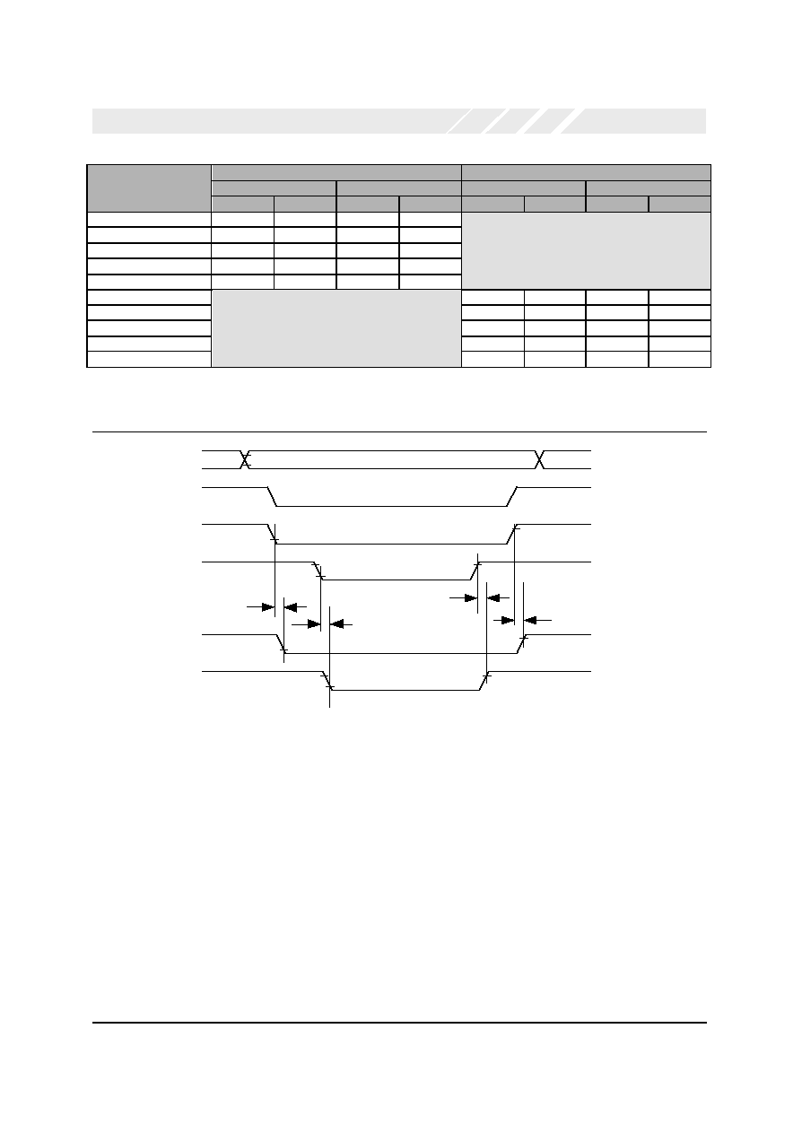
Page 55
OXCF950 DATA SHEET V1.1
OXFORD SEMICONDUCTOR LTD.
Read Access
Write Access
Min (ns)
Max (ns)
Min (ns)
Max (ns)
Symbol
3.3 v
5 v
3.3 v
5 v
3.3 v
5 v
3.3 v
5 v
t
su
A (IORD)
0
0
t
su
REG (IORD)
0
0
t
su
CE (IORD)
0
0
t
d
(IORD)
21
12
t
h
(IORD)
16
12
t
su
A (IOWR)
0
0
t
su
REG (IOWR)
0
0
t
su
CE (IOWR)
0
0
t
su
(IOWR)
0
0
t
h
(IOWR)
7
5
Table 51: I/O Access Timing Specification
10.4 Local Bus Access
OE#, WE#, IOWR#, RESET# = 1
A[3:0]
CE1#
IORD#
REG#
LB_CS#
LB_RD#
t
su
CE (LB_CS)
t
su
IORD (LB_RD)
t
d
IORD (LB_RD)
t
d
CE (LB_CS)
Figure 11: Local Bus read timing
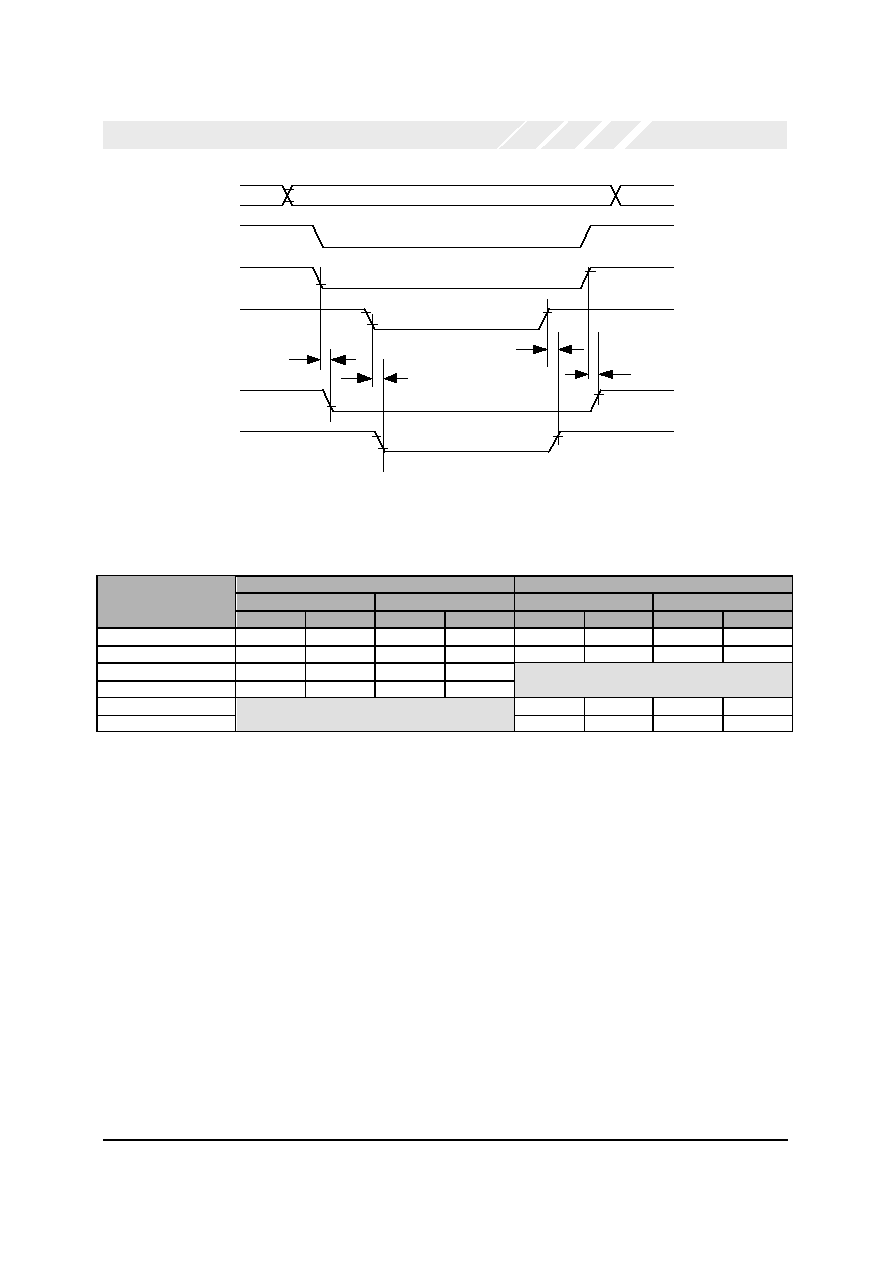
Page 56
OXCF950 DATA SHEET V1.1
OXFORD SEMICONDUCTOR LTD.
OE#, WE#, IORD#, RESET# = 1
A[3:0]
CE1#
IOWR#
REG#
LB_CS#
LB_WR#
t
su
CE (LB_CS)
t
su
IOWR (LB_WR)
t
d
IOWR (LB_WR)
t
d
CE (LB_CS)
Figure 12: Local Bus write timing
Read Access
Write Access
Min (ns)
Max (ns)
Min (ns)
Max (ns)
Symbol
3.3 v
5 v
3.3 v
5 v
3.3 v
5 v
3.3 v
5 v
t
su
CE (LB_CS)
10
7
10
7
t
d
CE (LB_CS)
10
7
10
7
t
d
IORD (LB_RD)
11
8
t
su
IORD (LB_RD)
11
8
t
d
IOWR (LB_WR)
10
7
t
su
IOWR (LB_WR)
10
7
Table 52: Local Bus Access Timing Specification
Note: The external local bus is only available in Local Bus mode.
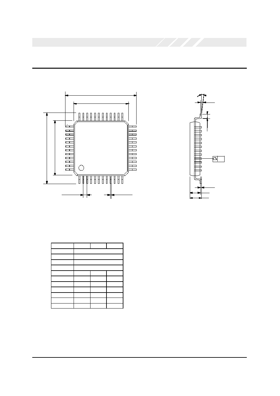
Page 57
OXCF950 DATA SHEET V1.1
OXFORD SEMICONDUCTOR LTD.
D
E
DL
A1
A2
A
EL
b
Ë
L
e
11
P
ACKAGE
I
NFORMATION
Figure 13: Device packaging
Dimension Min
Nom
Max
D
9.00 BSC
DL
7.00 BSC
E
9.00 BSC
EL
7.00 BSC
A
1.20
A1
0.05
0.15
A2
0.95
1.00
1.05
b
0.17
0.22
0.27
e
0.50
L
0.45
0.60
0.75
Ë
0.0∞
7.0∞
Table 53 : Package Dimensions
NOTE: All dimensions in millimetres. Angles in degrees.
#48
#1
DL

Page 58
OXCF950 DATA SHEET V1.1
OXFORD SEMICONDUCTOR LTD.
12 O
RDERING
I
NFORMATION
OX16 CF950-TQ - A
Revision
Package Type ≠ 48 TQFP

Page 59
OXCF950 DATA SHEET V1.1
OXFORD SEMICONDUCTOR LTD.
N
OTES
This page has been intentionally left blank

Page 60
OXCF950 DATA SHEET V1.1
OXFORD SEMICONDUCTOR LTD.
C
ONTACT
D
ETAILS
Oxford Semiconductor Ltd.
25 Milton Park
Abingdon
Oxfordshire
OX14 4SH
United Kingdom
Telephone:
+44 (0)1235 824900
Fax:
+44 (0)1235 821141
Sales e-mail:
sales@oxsemi.com
Web site:
http://www.oxsemi.com
D
ISCLAIMER
Oxford Semiconductor believes the information contained in this document to be accurate and reliable. However, it is subject to
change without notice. No responsibility is assumed by Oxford Semiconductor for its use, nor for infringement of patents or other
rights of third parties. No part of this publication may be reproduced, or transmitted in any form or by any means without the prior
consent of Oxford Semiconductor Ltd. Oxford Semiconductor's terms and conditions of sale apply at all times.