 | –≠–ª–µ–∫—Ç—Ä–æ–Ω–Ω—ã–π –∫–æ–º–ø–æ–Ω–µ–Ω—Ç: OZ965R | –°–∫–∞—á–∞—Ç—å:  PDF PDF  ZIP ZIP |
OZ965
06/20/00
OZ965-SF-3.0
Page 1
Copyright 2000 by O
2
Micro
All Rights Reserved
U.S. Patent #5,619,402
High-Efficiency Inverter Controller
FEATURES
∑
Single-stage power conversion, requiring
only a +5 V voltage source
∑
Reduces the number of components and
board size by 30% compared with
conventional design
∑
Supports both floating and grounded
secondary designs
∑
90% efficiency vs. typical 75% efficiency of
conventional designs
∑
Internal open-lamp and short-circuit
protections
∑
Wide dimming range
∑
Supports multiple CCFLs
∑
Simple and reliable 2-winding transformer
design
∑
Eliminates leakage current when used in a
floating secondary design
∑
Constant-frequency design eliminates
interference with LCDs
ORDERING INFORMATION
OZ965G - 16-pin plastic SOP
OZ965R - 16-pin plastic TSSOP
OZ965
I
G - 16-pin plastic SOP
OZ965
I
R - 16-pin plastic TSSOP
GENERAL DESCRIPTION
The OZ965 is a single chip, high-efficiency, Cold
Cathode Fluorescent Lamp (CCFL) backlight
inverter controller whose primary function is to
convert +5 volt DC power to approximately 600
VAC. Additionally, the OZ965 performs the lamp
dimming function with an analog voltage or low
frequency Pulse Width Modulation (PWM)
control.
Operating Principle:
The CCFL tube, transformer secondary, and
capacitor form a resonant circuit. The OZ965
utilizes the low energy loss resonate mode
principle to deliver a very high efficiency inverter.
The OZ965 drives the transformer primary with a
variable pulse width voltage directly from the +5v
supply. The resultant primary drive current is
alternately reversing with zero-voltage-switching.
Because of the transformer leakage inductance
and the secondary resonant circuit, the
secondary voltage and current are approximately
sinusoidal. This sinusoid results in very little
harmonic emi/rfi emissions.
The OZ965 operates at a single, constant
frequency in a PWM mode. Typical operating
frequency ranges between 30 KHz to 200 KHz,
dependent upon the CCFL and transformer
characteristics. Intelligent open-lamp protection
provides design flexibility so various transformer
models/manufacturers may be used.
Its high driving capability allows the OZ965 to
drive high power MOSFETs.
The single stage design results in a low cost,
reliable transformer without expensive, less
reliable secondary fold-back treatment. The
transformer does not require a more expensive
center tapped primary.
The OZ965 is available in 16-pin SOP and
TSSOP packages. It is specified over the
commercial temperature range of 0
∞
C to +70
∞
C,
and the industrial temperature range of -40
∞
C to
+85
∞
C.
CR3
BAV99L
1
3
2
C3
10u
C6
470p
C9
0.01u
R6
59.0k
R3
150k
U1
OZ965
REF
1
HCLMP
2
SCP
4
ADJ
5
FB
6
CMP
7
GND
8
SST
9
PDR
10
NDR
11
ENA
12
OPS
13
CT
14
RT
15
VDD
16
LCLMP
3
R15
4.3k
C11
0.1u
R13
510k
C2
22u
C7
10u
R2
22
R4
20k
R5
15k
C4
0.1u
C8
0.1u
T1
17:2200
2
7
5
6
U2
Si4532
2
1
4
3
5
6
7
8
C1
0.1u
C10
2.2u
R1
100k
J1
5V
1
5V
2
ENA
3
DIM
4
GND
5
GND
6
C12
0.1u
R16
100k
R17
1.02k
C5
68p 3kv
J2
HV
1
RTN
2
Q1
Q2
Figure 1. Typical Application Circuit

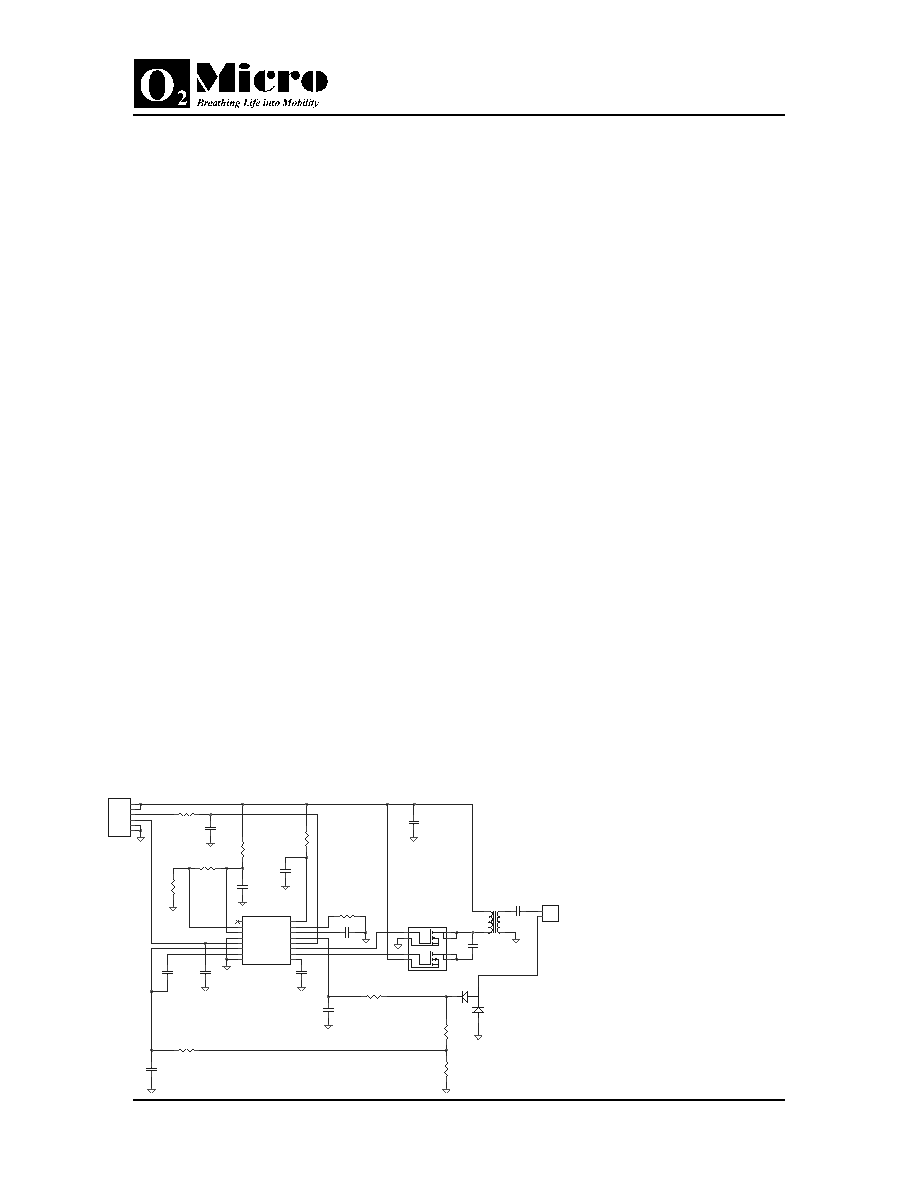
OZ965
OZ965-SF-3.0
Page 2
FUNCTIONAL BLOCK
DIAGRAM
Refer to the functional block diagram in Figure 2,
below, and the Pin Description Table on page 3.
Power is transferred to the transformer primary
by the N-MOSFET, driven by the MOSFET gate
driver out of pin NDR. The P-MOSFET resets the
primary field, driven by pin PDR. The usual
design results in approximately 50% duty cycle at
full lamp intensity. Terminating the NDR signal
earlier than the full brightness lamp pulse width
performs lamp dimming, using the analog
dimming. The voltages on pins HCLMP and
LCLMP set a threshold voltage for the ramp
comparator setting the maximum duty cycle for
NDR.
A pulse generator circuit creates the clock signal
with the frequency determined by an external,
constant current setting resistor (RT) and timing
capacitor (CT).
The "soft-start" circuit ensures a reliable and long
lamp life starting condition.
"Soft start" gradually increases the energy
delivered to the secondary.
When the OZ965 is enabled at pin ENA, the
capacitor on pin SST determines the duration of
the "soft-start" period, gradually increasing the
NDR pulse width to the regulated brightness. The
"soft-start" period provides sufficient time for the
lamp to ignite.
For system reliability there are several circuit
protections provided. To ensure a controlled
output, the secondary current is monitored on pin
FB and is compared to a reference voltage on pin
ADJ. The NDR signal is shortened or lengthened
dependent upon this feedback. Protection is
provided by the resultant signal, CMP, monitoring
for a lamp removal condition. Short circuit
protection is provided at pin SCP. The OPS
signal selects either HCLMP or LCLMP providing
current protection against an "Open Lamp"
condition at start-up. The OPS signal also allows
adjustment to different transformer models.
To reduce power dissipation, the switch
(MOSFET) drive signals are "break-before-make"
with a short, fixed off time between activation of
NDR or PDR.
Note:
OVP ≠ Over Voltage Protection
SCP ≠ Short-Circuit Protection
UVL ≠ Under Voltage Lockout
Figure 2. Functional Block Diagram
SCP
NDRV
ZVS
CONTROLLER
PDRV
SST
NDR
PDR
Vdd
ENA
OPS
CT
RT
REF
IBIAS
&
REFERENCE
2.50V
HCLMP
LCLMP
ADJ
FB
CMP
GND
PULSE GEN
ACTIVE
"HIGH"
-
EA
+
-
+
LAMP
ON/OFF
Vmax
Vmin
(fix value)
V
V>Vmax -- -> Vmax
Vmin<V<Vmax ->V
V<Vmin -- ->Vmin
UNDER VOLTAGE
LOCKOUT
t1+t2
(slow start)
PROTECTION
+
-
COMP
COMP
COMP
COMP
t1
(slow start)
RAMP
COMP.
Vmax=2.6V-Vset
COMP
Vset
3
4
2
5
6
7
1
10
16
15
14
13
12
11
9
8
POFF
POFF
2.5V
0.5V
CLK
0.6V
RA
M
P
CO
M
P
.
P
U
LS
E
SS2
UVLO
OLPROT
PO
F
F
ENABLE
Pgate
2.5V
Ngate
RESET
SS1
Vdd
1.5V
SS1
V_SS2
MN1
R2
4K
I=2.5uA
I=12uA
R4
70k
R5
630k
-
+
-
+
-
+
-
+
-
+
R1
300k
OZ965
OZ965-SF-3.0
Page 3
PIN DESCRIPTION
Names Pin
No. I/O
Description
REF
1
O
Reference voltage output. Nominal voltage is 2.5 V.
HCLMP
2
I
Clamping maximum duty cycle under normal operation.
LCLMP
3
I
Clamping maximum duty cycle under open-lamp condition.
SCP
4
I
Short-circuit protection input (V
TH
=0.6V)
ADJ
5
I
Reference voltage input for dimming control.
FB
6
I
Current sense feedback.
CMP
7
O
Compensation for the current sense feedback.
GND 8
GND
Ground.
SST
9
I
Soft-start ensures lamp current pulses gradually increases to its normal
value
PDR
10
O
Gate drive output for the P-MOSFET.
NDR
11
O
Gate drive output for the N-MOSFET.
ENA
12
I
Enable input, active high (V
TH
=1.5V)
OPS
13
I
Output current sense (V
TH
=0.6V)
CT
14
I/O
Timing capacitor. CT and RT set the clock frequency.
RT 15
I/O
Timing resistor. Fosc = 1.91 / (Rt
∑
Ct)
VDD
16
PWR
Supply voltage input.
ABSOLUTE MAXIMUM RATINGS
VDD
5.5V
GND
+/- 0.3V
Logic inputs
-0.3 V to VDD+0.3V
OZ965
OZ965I
Operating temp.
0
o
C to 70
o
C -40
o
C to 85
o
C
Operating junction temp.
150
o
C
Storage temp.
-55
o
C to 150
o
C
OZ965
OZ965I
Power dissipation
-
16-pin SOP
-
16-pin TSSOP
.720W
.690W
.580W
.550W
Thermal Impedance
-
16-pin SOP
-
16-pin TSSOP
111
o
C/W
115
o
C/W
111
o
C/W
115
o
C/W
RECOMMENDED OPERATING RANGE
VDD
5.0 V +/- 5%
Fosc
30 KHz to 200 KHz
Rosc
50 k to 150 k

OZ965
OZ965-SF-3.0
Page 4
FUNCTIONAL SPECIFICATIONS
Parameter
Symbol
Test Conditions
Limits
Unit
4.75 V < VDD < 5.25 V
Min
Typ
Max
Reference Voltage
Nominal voltage
Vref
I
load
= 0.1 mA,
2.37
2.50
2.63
V
Line regulation
-
6
-
mV/V
Load regulation
I
load
= 0.2 mA to 1.0 mA
-
1
-
mV/mA
Oscillator
Initial accuracy
fosc
Ct = 470 pF, Rt = 49.9 k
81
KHz
Ramp peak
-
2.54
-
V
Ramp valley
-
0.48
-
V
Temp. stability
TA = -40
o
C to 85
o
C -
-
200
ppm/
o
C
Error Amplifier
Input bias current
ADJ=FB=2.0 V
-
0.25
-
uA
Input offset voltage
VFB = 4.0 V
5
10
mV
Input voltage range
0
-
VDD-
1.5
V
Open loop voltage gain
-
65
-
dB
Unity gain bandwidth
-
1.5
-
MHz
Power supply rejection
-
60
-
dB
Under-Voltage Lockout
Positive-going threshold voltage
See Table 1, page 5
Negative-going threshold voltage
See Table 1, page 5
Supply
Supply current - Enable Low
I
OFF
-
195
-
µ
A
Supply current - Enable High
I
ON
VDD
= 5.0 V
-
1.0
-
mA
NDR output
Output high voltage
V
OH
Isource = 10 mA, VDD = 5V
-
4.75
-
V
Output low voltage
V
OL
Isink = 10 mA, VDD = 5V
-
0.25
0.5
V
Output resistance
R
OUT
-
10
-
PDR output
Output high voltage
V
OH
Isource = 10 mA, VDD = 5V
-
4.7
-
V
Output low voltage
V
OL
Isink = 10 mA, VDD = 5V
-
0.5
-
V
Output resistance
R
OUT
-
15
-
Break-Before-Make
Qn off to Qp on delay
T
HL
-
250
-
ns
Qp off to Qn on delay
T
LH
-
220
-
Ns
High Clamp
OPS=1 V V
HCLMP
=0V 92
94
96
Duty cycle of NDR
HCLMP
OPS=1 V, V
HCLMP
=1.8V -
14
-
%
Low Clamp
OPS=0 V, V
LCLMP
=0V 92
94
96
Duty cycle of NDR
LCLMP
OPS=0 V, V
LCLMP
=1.8V -
14
-
%
Max. / Min. Duty cycle
Duty cycle of NDR
6
-
95
%

OZ965
OZ965-SF-3.0
Page 5
OZ965
OZ965
I
Parameter
Test Conditions
Limits
Unit
Limits
Unit
4.75V < VDD < 5.25V
Min
Typ Max Min Typ Max
Under-Voltage Lockout
Positive-going threshold voltage
- 3.9 4.3 V -
3.9
4.5
V
Negative-going threshold voltage
3.2 3.4 - V 3.0
3.4
-
V
Table 1. Under-Voltage Lockout for OZ965 and OZ965
I
OZ965
OZ965-SF-3.0
Page 6
PACKAGE INFORMATION
TSSOP-16
PACKAGE
E1
E
D
e
b
A
A2
A1
L1
Gauge Plane
2
1
3
L
R1
R
b
c1
b1
c
1
16
Lead Cross Section
INCHES MILLIMETERS
DIM
MIN MAX MIN MAX
A -
0.043
-
1.20
A1 0.002
0.006 0.05 0.15
A2 0.031
0.041 0.80 1.05
L 0.020
0.030
0.45 0.75
D - -
4.90
5.10
E1 0.169
0.177 4.30 4.50
E 0.252BSC 6.40BSC
R 0.004 - 0.09 -
R1 0.004 - 0.09 -
b 0.007
0.012
0.19
0.30
b1 0.007
0.010
0.19 0.25
c 0.004
0.008
0.09
0.20
c1 0.004
0.006
0.09 0.16
L1 0.039REF
1.0REF
e 0.026BSC 0.65BSC
1 0
∞
8
∞
0
∞
8
∞
2 12
∞
REF 12
∞
REF
3
12
∞
REF 12
∞
REF

OZ965
OZ965-SF-3.0
Page 7
H
E
A
A1
e
B
D
SOP-16
PACKAGE
C
L
D
INCHES MILLIMETERS
DIM
MIN MAX MIN MAX
A 0.0532
0.0688
1.35 1.75
A1 0.0040
0.0098 0.10 0.25
B 0.013
0.020
0.33 0.51
C 0.0075
0.0098
0.19 0.25
D 0.3859
0.3937
9.80 10.00
E 0.1497
0.1574
3.80 4.00
e
0.050 BCS.
1.27 BCS.
H 0.2284
0.244
0
5.80 6.20
L 0.016
0.050
0.40
1.27
0
∞
8
∞
0
∞
8
∞