QL2003
3-6
The QL2003 is a 3,000 usable ASIC gate, 5,000 usable PLD gate member of
the pASIC 2 family of FPGAs. pASIC 2 FPGAs employ a unique
combination of architecture, technology, and software tools to provide high
speed, high usable density, low price, and flexibility in the same devices.
The flexibility and speed make pASIC 2 devices an efficient and high
performance silicon solution for designs described using HDLs such as
Verilog and VHDL, as well as schematics.
The QL2003 contains 192 logic cells. With 118 maximum I/Os, the
QL2003 is available in 84-PLCC, 100-pin TQFP and 144-pin TQFP
packages.
Software support for the complete pASIC families, including the QL2003, is
available through three basic packages. The turnkey QuickWorks
Æ
package
provides the most complete FPGA software solution from design entry to
logic synthesis (by Synplicity, Inc.), to place and route, to simulation. The
QuickTools
TM
and QuickChip
TM
packages provide a solution for designers
who use Cadence, Mentor, Synopsys, Viewlogic, Veribest, or other third-
party tools for design entry, synthesis, or simulation.
Total of 118 I/O Pins
- 110 bidirectional input/output pins, PCI-compliant at 5.0V
in -1/-2 speed grades
- 4 high-drive input-only pins
- 4 high-drive input/distributed network pins
Four Low-Skew (less than 0.5ns) Distributed Networks
- Two array networks available to logic cell flip-flop clock, set, and
reset - each driven by an input-only pin
- Two global clock/control networks available to F1 logic input, and
logic cell flip-flop clock, set, reset; input and I/O register clock, reset,
enable; and output enable controls - each driven by an input-only pin,
or any input or I/O pin, or any logic cell output or I/O cell feedback
High Performance
- Input + logic cell + output delays under 6 ns
- Datapath speeds exceeding 225 MHz
- Counter speeds over 200 MHz
PRODUCT
SUMMARY
FEATURES
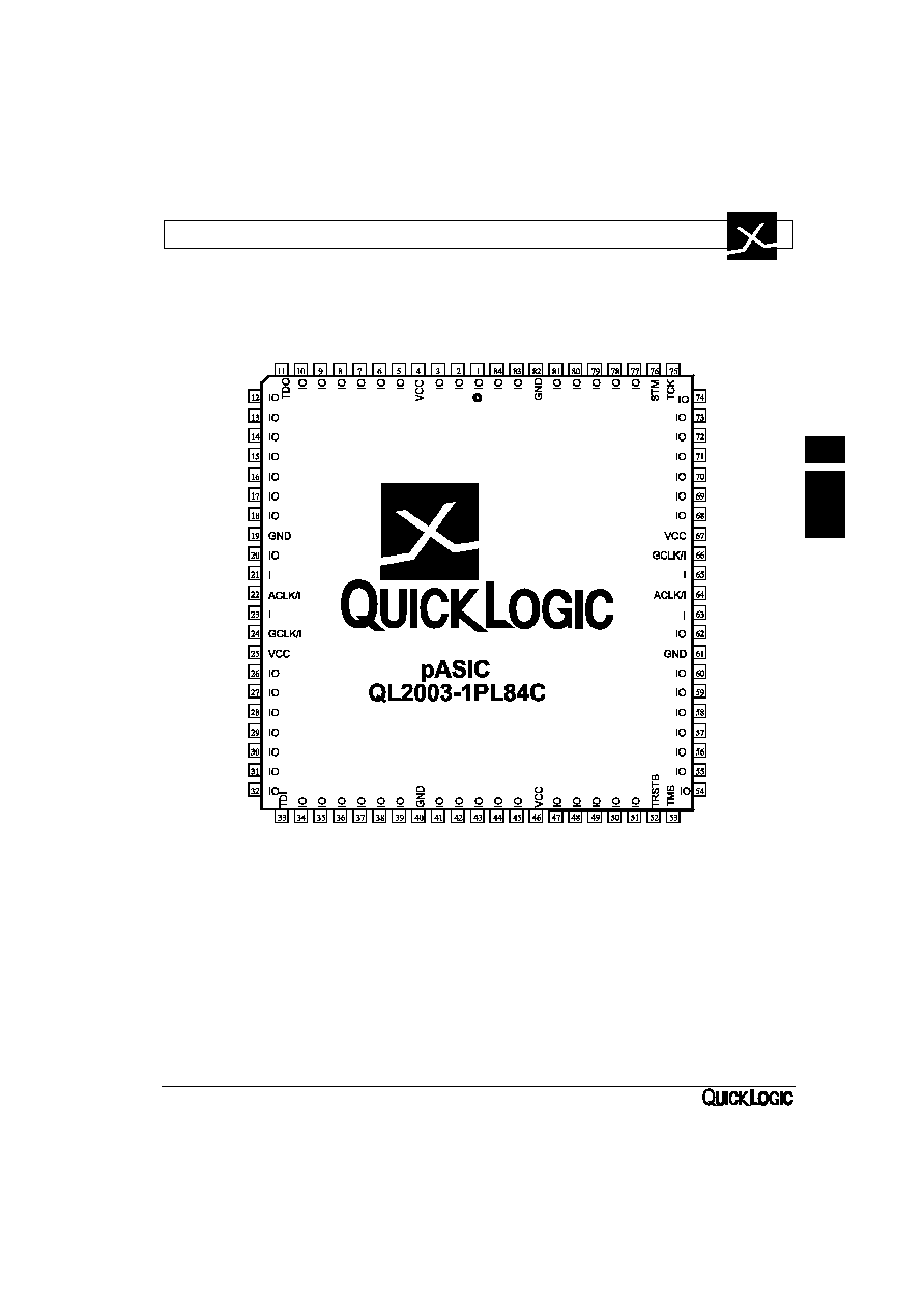
QL2003
3-7
PINOUT DIAGRAM
84-PIN PLCC
pAS
I
C 2
3

QL2003
3-8
PINOUT DIAGRAMS
100-PIN TQFP
pASIC
QL2003-1PF100C
144-PIN TQFP
pASIC
QL2003-1PF144C
PIN # 1
PIN # 109
PIN # 37
PIN # 73
PIN # 1
PIN # 76
PIN # 26
PIN # 51
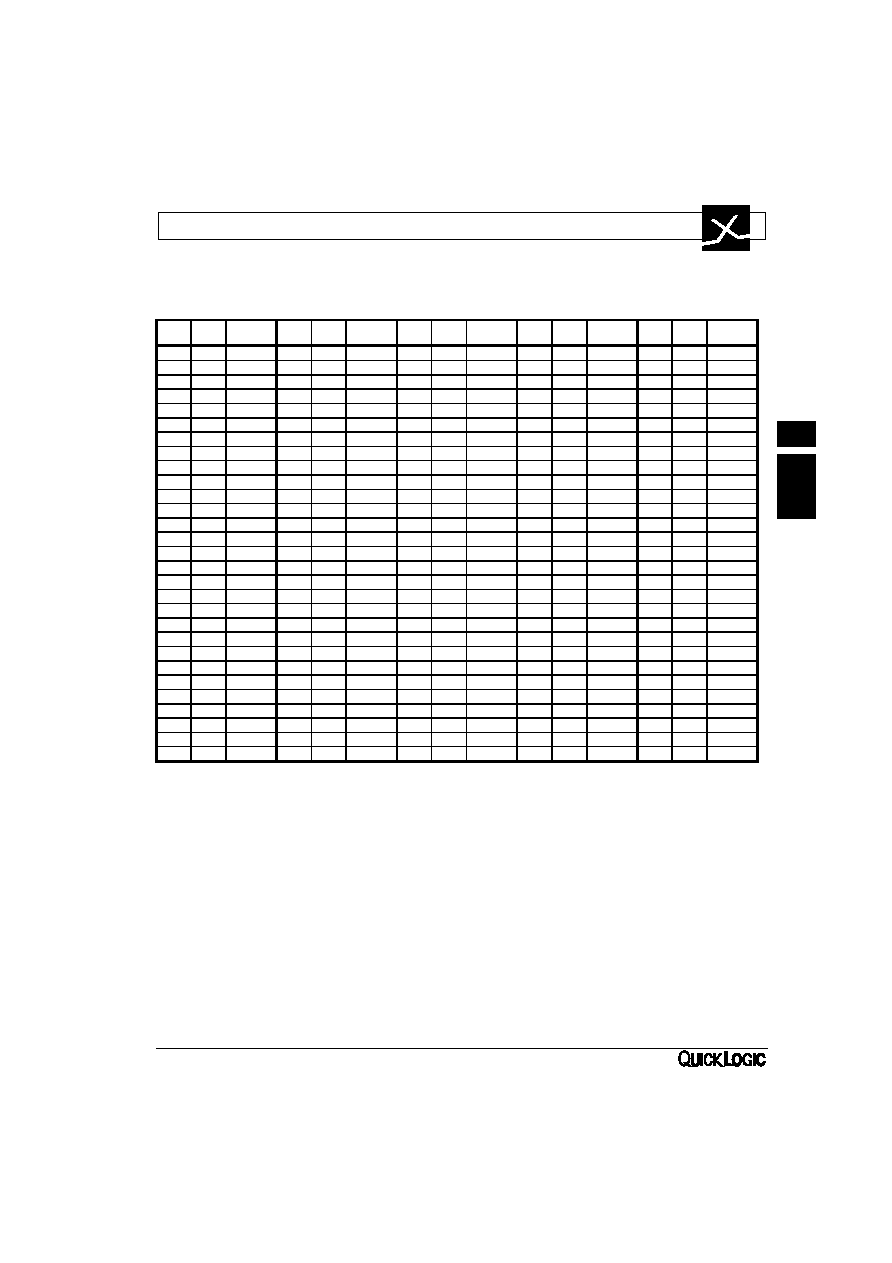
QL2003
3-9
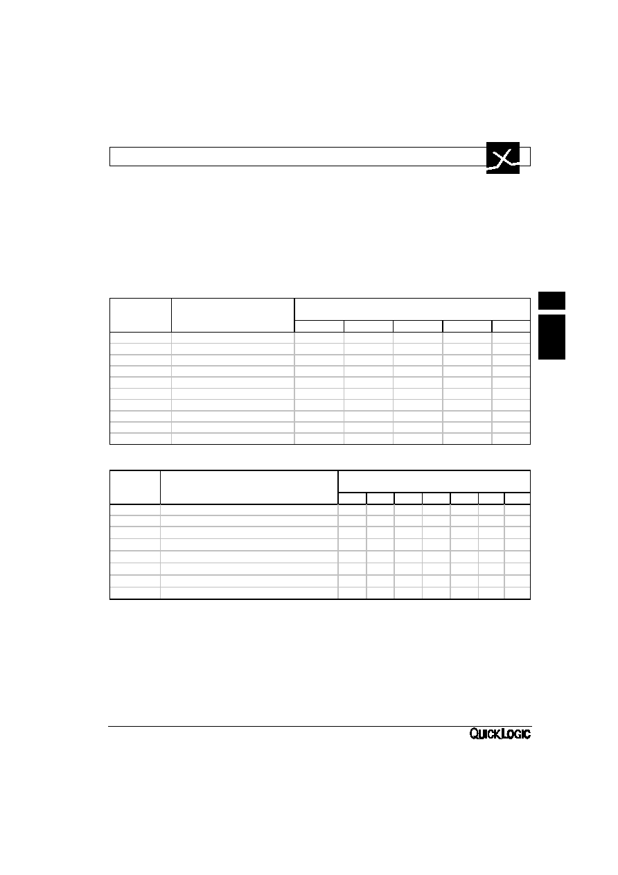
100 and 144 TQFP Pinout Table
144
TQFP
100
TQFP
Function
144
TQFP
100
TQFP
Function
144
TQFP
100
TQFP
Function
144
TQFP
100
TQFP
Function
144
TQFP
100
TQFP
Function
1
2
I/O
30
NC
GND
59
NC
I/O
88
60
I/O
116
82
I/O
2
NC
I/O
31
NC
I/O
60
43
I/O
89
61
I
117
83
I/O
3
3
I/O
32
22
I/O
61
44
I/O
90
62
ACLK / I
118
NC
I/O
4
4
I/O
33
NC
I/O
62
45
I/O
91
63
VCC
119
84
I/O
5
NC
I/O
34
23
I/O
63
NC
I/O
92
64
I
120
NC
I/O
6
5
I/O
35
NC
I/O
64
NC
I/O
93
65
GCLK / I
121
NC
I/O
7
NC
VCC
36
24
I/O
65
46
I/O
94
66
VCC
122
85
GND
8
6
I/O
37
25
I/O
66
NC
GND
95
67
I/O
123
NC
I/O
9
NC
I/O
38
26
TDI
67
NC
I/O
96
NC
I/O
124
86
I/O
10
7
I/O
39
27
I/O
68
NC
I/O
NC
68
I/O
125
87
I/O
11
NC
I/O
40
28
I/O
69
47
I/O
97
NC
I/O
126
88
GND
12
NC
I/O
41
29
I/O
70
48
I/O
98
69
I/O
127
89
I/O
13
8
I/O
42
NC
VCC
71
49
TRSTB
99
NC
I/O
128
90
I/O
14
NC
I/O
43
30
I/O
72
50
TMS
100
70
I/O
129
91
I/O
15
9
GND
44
31
I/O
73
51
I/O
101
71
I/O
130
92
VCC
16
10
I/O
45
NC
I/O
74
52
I/O
102
NC
GND
131
NC
I/O
17
11
I
46
32
I/O
75
53
I/O
103
NC
I/O
132
93
I/O
18
12
ACLK / I
47
33
I/O
76
54
I/O
104
72
I/O
133
NC
I/O
19
13
VCC
48
NC
I/O
77
55
I/O
105
NC
I/O
134
94
I/O
20
14
I
49
34
I/O
78
NC
I/O
106
73
I/O
135
NC
I/O
21
15
GCLK / I
50
35
GND
79
NC
VCC
107
74
I/O
136
NC
I/O
22
16
VCC
51
36
I/O
80
NC
I/O
108
75
I/O
137
95
I/O
23
17
I/O
52
NC
I/O
81
56
I/O
109
76
TCK
138
NC
GND
24
18
I/O
53
37
I/O
82
NC
I/O
110
77
STM
139
96
I/O
25
NC
I/O
54
38
GND
83
57
I/O
111
78
I/O
140
97
I/O
26
19
I/O
55
39
I/O
84
NC
I/O
112
79
I/O
141
98
I/O
27
NC
I/O
56
40
I/O
85
58
I/O
113
80
I/O
142
99
I/O
28
20
I/O
57
41
I/O
86
NC
I/O
114
NC
VCC
143
100
TDO
29
21
I/O
58
42
VCC
87
59
GND
115
81
I/O
144
1
I/O
pAS
I
C 2
3

QL2003
3-10
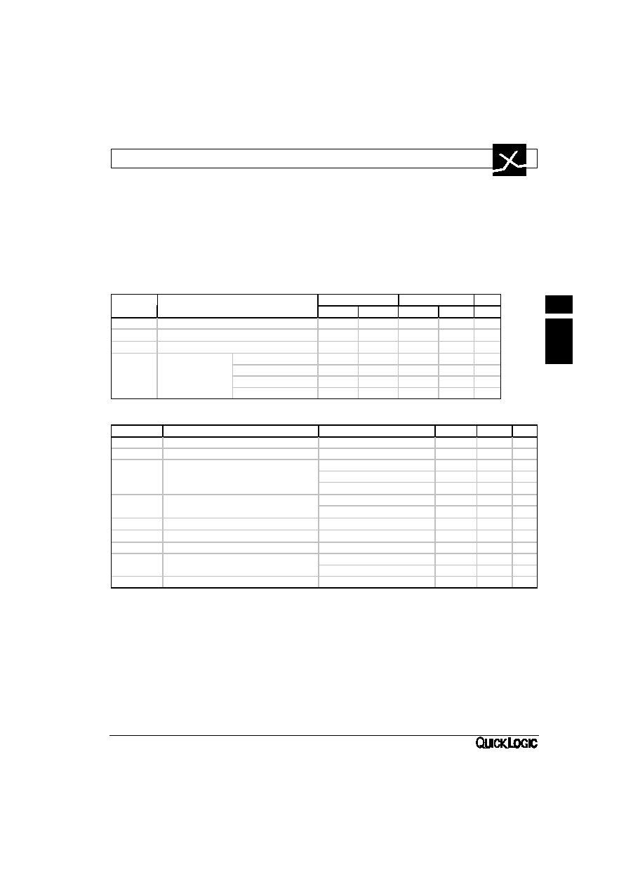
PIN DESCRIPTIONS
Pin
Function
Description
TDI
Test Data In for JTAG
Hold HIGH during normal operation. Connect to
VCC if not used for JTAG.
TRSTB
Active low Reset for JTAG
Hold LOW during normal operation. Connect to
ground if not used for JTAG.
TMS
Test Mode Select for JTAG
Hold HIGH during normal operation. Connect to
VCC if not used for JTAG.
TCK
Test Clock for JTAG
Hold HIGH or LOW during normal operation.
Connect to VCC or ground if not used for JTAG.
TDO
Test data out for JTAG
Output that must be left unconnected if not used for JTAG.
STM
Special Test Mode
Must be grounded during normal operation.
I/ACLK
High-drive input and/or array
network driver
Can be configured as either or both.
I/GCLK
High-drive input and/or global
network driver
Can be configured as either or both.
I
High-drive input
Use for input signals with high fanout.
I/O
Input/Output pin
Can be configured as an input and/or output.
VCC
Power supply pin
Connect to 3.3V supply.
GND
Ground pin
Connect to ground.
ORDERING
INFORMATION
QL 2003 - 1 PF100 C
QuickLogic
pASIC device
pASIC 2 device
part number
Speed Grade
X = quick
0 = fast
1 = faster
2 = fastest
Operating Range
C = Commercial
I = Industrial
Package Code
PL84 = 84-pin PLCC
PF100 = 100-pin TQFP
PF144 = 144-pin TQFP
QL2003
3-11
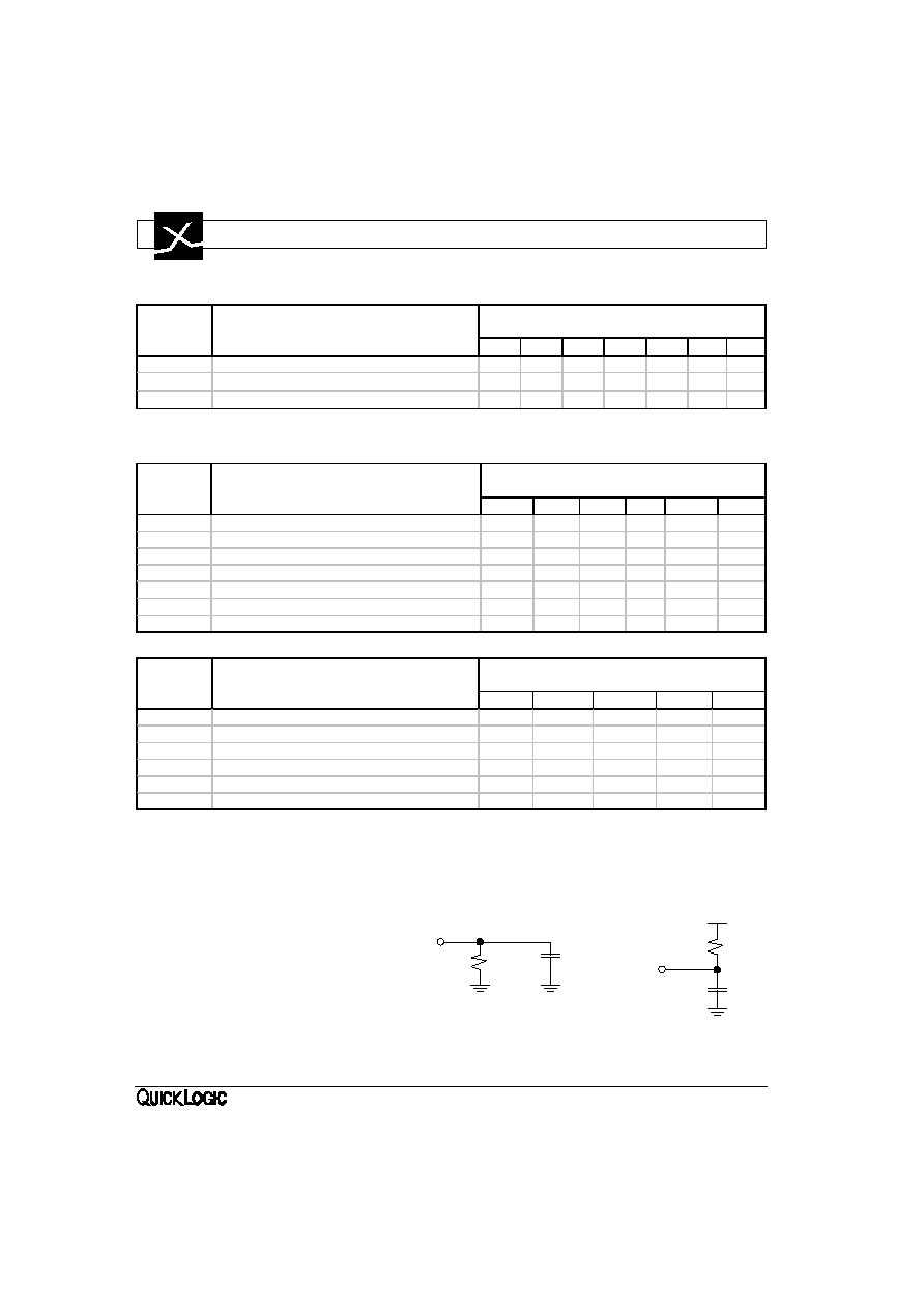
ABSOLUTE MAXIMUM RATINGS
Supply Voltage .................... -0.5 to 7.0V
Storage Temperature................ -65
∞
C to + 150
∞
C
Input Voltage ............. -0.5 to VCC +0.5V
Lead Temperature ................................ 300
∞
C
ESD Pad Protection ...................
±
2000V
DC Input Current ......................
±
20 mA
Latch-up Immunity ...................
±
200 mA
5 Volt OPERATING RANGE
Symbol
Parameter
Industrial
Commercial
Unit
Min
Max
Min
Max
VCC
Supply Voltage
4.5
5.5
4.75
5.25
V
TA
Ambient Temperature
-40
85
0
70
∞
C
TC
Case Temperature
∞
C
-X Speed Grade
0.4
2.75
0.46
2.55
K
Delay Factor
-0 Speed Grade
0.4
2.00
0.46
1.85
-1 Speed Grade
0.4
1.61
0.46
1.50
-2 Speed Grade
0.4
1.35
0.46
1.25
DC CHARACTERISTICS over 5V operating range
Symbol
Parameter
Conditions
Min
Max
Unit
VIH
Input HIGH Voltage
2.0
V
VIL
Input LOW Voltage
0.8
V
IOH = -4 mA
3.7
V
VOH
Output HIGH Voltage
IOH = -24 mA/-16 mA [1]
2.4
V
IOH = -10
µ
A
VCC-0.1
V
VOL
Output LOW Voltage
IOL = 24 mA/16 mA [1]
0.45
V
IOL = 10
µ
A
0.1
V
II
Input Leakage Current
VI = VCC or GND
-10
10
µ
A
IOZ
3-State Output Leakage Current
VI = VCC or GND
-10
10
µ
A
CI
Input Capacitance [2]
10
pF
IOS
Output Short Circuit Current [3]
VO = GND
-15
-120
mA
VO = VCC
40
210
mA
ICC
D.C. Supply Current [4]
VI, VIO = VCC or GND
2 (typ)
10
mA
Notes:
[1]
-24 mA IOH and 24 mA IOL apply only to -1/-2 commercial grade devices. These speed grades are
also PCI-compliant. All other devices have -16 mA IOH and 16 mA IOL specifications.
[2]
Capacitance is sample tested only.
[3]
Only one output at a time. Duration should not exceed 30 seconds.
[4]
For -0/-1/-2 commercial grade devices only. Maximum ICC is 20 mA for -X commercial grade
devices and 15mA for all industrial grade devices. For AC conditions, contact QuickLogic customer
engineering.
pAS
I
C 2
3

QL2003
3-12
3.3 Volt
OPERATING RANGE
Symbol
Parameter
Industrial
Commercial
Unit
Min
Max
Min
Max
VCC
Supply Voltage
3.0
3.6
3.0
3.6
V
TA
Ambient Temperature
-40
85
0
70
∞
C
-0 Speed Grade
0.56
2.74
0.61
2.65
K
Delay Factor
-1 Speed Grade
0.56
2.21
0.61
2.14
-2 Speed Grade
0.56
1.85
0.61
1.79
DC CHARACTERISTICS over 3.3V operating range
Symbol
Parameter
Conditions
Min
Max
Unit
VIH
Input HIGH Voltage
2.0
V
VIL
Input LOW Voltage
0.8
V
VOH
Output HIGH Voltage
IOH = -2.4 mA
2.4
V
IOH = -10
µ
A
VCC-0.1
V
VOL
Output LOW Voltage
IOL = 4 mA
0.4
V
IOL = 10
µ
A
0.1
V
IIH
Input High Current Sink
(for tolerance to 5V devices)
5.5V > VI > VCC
12
mA
II
Input Leakage Current
VI = VCC or GND
-10
10
µ
A
IOZ
3-State Output Leakage Current
VI = VCC or GND
-10
10
µ
A
CI
Input Capacitance [5]
10
pF
IOS
Output Short Circuit Current [6]
VO = GND
-10
-70
mA
VO = VCC
25
130
mA
ICC
D.C. Supply Current [7]
VI, VIO = VCC or GND
0.5 (typ)
3
mA
Notes:
[5]
Capacitance is sample tested only.
[6]
Only one output at a time. Duration should not exceed 30 seconds.
[7]
For commercial grade devices only. Maximum ICC is 5 mA for all industrial grade devices. For AC
conditions, contact QuickLogic customer engineering.
QL2003
3-13
AC CHARACTERISTICS at VCC = 5V, TA = 25
∞
∞
C (K = 1.00)
Propagation delays depend on routing, fanout, load capacitance, supply voltage, junction temperature,
and process variation. The AC Characteristics are a design guide to provide initial timing estimates at
nominal conditions. Worst case estimates are obtained when nominal propagation delays are multiplied
by the appropriate Delay Factor, K, as specified in the Delay Factor table (Operating Range). The
QuickChip/QuickTools/QuickWorks software incorporates data sheet AC Characteristics into the
design database for precise path analysis or simulation results following place and route.
Logic Cells
Input-Only Cells
Symbol
Parameter
Propagation Delays (ns)
Fanout [8]
1
2
3
4
8
12
24
tIN
High Drive Input Delay
2.5
2.6
2.6
2.7
3.5
4.6
5.8
tINI
High Drive Input, Inverting Delay
2.6
2.7
2.7
2.8
3.6
4.7
5.9
tISU
Input Register Set-Up Time
4.8
4.8
4.8
4.8
4.8
4.8
4.8
tIH
Input Register Hold Time
0.0
0.0
0.0
0.0
0.0
0.0
0.0
tlCLK
Input Register Clock To Q
0.9
1.0
1.0
1.1
1.9
3.0
4.2
tlRST
Input Register Reset Delay
0.8
0.9
0.9
1.0
1.8
2.9
4.1
tlESU
Input Register clock Enable Set-Up Time
4.1
4.1
4.1
4.1
4.1
4.1
4.1
tlEH
Input Register Clock Enable Hold Time
0.0
0.0
0.0
0.0
0.0
0.0
0.0
Notes:
[8]
Stated timing for worst case Propagation Delay over process variation at VCC=5.0V and TA=25
∞
C.
Multiply by the appropriate Delay Factor, K, for speed grade, voltage and temperature settings as
specified in the Operating Range.
[9]
These limits are derived from a representative selection of the slowest paths through the pASIC 2 logic
cell including typical net delays. Worst case delay values for specific paths should be determined from
timing analysis of your particular design.
Symbol
Parameter
Propagation Delays (ns)
Fanout [8]
1
2
3
4
8
tPD
Combinatorial Delay [9]
1.4
1.7
2.0
2.3
3.5
tSU
Setup Time [9]
1.8
1.8
1.8
1.8
1.8
tH
Hold Time
0.0
0.0
0.0
0.0
0.0
tCLK
Clock to Q Delay
0.8
1.1
1.4
1.7
2.9
tCWHI
Clock High Time
2.0
2.0
2.0
2.0
2.0
tCWLO
Clock Low Time
2.0
2.0
2.0
2.0
2.0
tSET
Set Delay
1.4
1.7
2.0
2.3
3.5
tRESET
Reset Delay
1.2
1.5
1.8
2.1
3.3
tSW
Set Width
1.9
1.9
1.9
1.9
1.9
tRW
Reset Width
1.8
1.8
1.8
1.8
1.8
pAS
I
C 2
3
QL2003
3-14
Clock Cells
Symbol
Parameter
Propagation Delays (ns)
Loads per Half Column [10]
1
2
3
4
8
10
13
tACK
Array Clock Delay
2.2
2.2
2.3
2.4
2.5
2.6
tGCKP
Global Clock Pin Delay
1.2
1.2
1.2
1.2
1.2
1.2
1.2
tGCKB
Global Clock Buffer Delay
1.5
1.6
1.6
1.7
1.8
1.9
2.0
I/O Cells
Symbol
Parameter
Propagation Delays (ns)
Fanout [8]
1
2
3
4
8
10
tI/O
Input Delay (bidirectional pad)
1.8
2.1
2.4
2.7
3.9
4.6
tISU
Input Register Set-Up Time
4.8
4.8
4.8
4.8
4.8
4.8
tIH
Input Register Hold Time
0.0
0.0
0.0
0.0
0.0
0.0
tlOCLK
Input Register Clock To Q
0.8
1.1
1.4
1.7
2.9
3.6
tlORST
Input Register Reset Delay
0.7
1.0
1.3
1.6
2.8
3.5
tlESU
Input Register clock Enable Set-Up Time
4.1
4.1
4.1
4.1
4.1
4.1
tlEH
Input Register Clock Enable Hold Time
0.0
0.0
0.0
0.0
0.0
0.0
Symbol
Parameter
Propagation Delays (ns)
Output Load Capacitance (pF)
30
50
75
100
150
tOUTLH
Output Delay Low to High
2.6
3.0
3.6
4.1
5.2
tOUTHL
Output Delay High to Low
2.8
3.3
3.9
4.5
5.7
tPZH
Output Delay Tri-state to High
2.1
2.6
3.1
3.7
4.8
tPZL
Output Delay Tri-state to Low
2.6
3.3
4.1
4.9
6.5
tPHZ
Output Delay High to Tri-State [11]
2.9
tPLZ
Output Delay Low to Tri-State [11]
3.3
Notes:
[10]
The array distributed networks consist of 48 half columns and the global distributed networks consist of
52 half columns, each driven by an independent buffer. The number of half columns used does not affect
clock buffer delay. The array clock has up to 10 loads per half column. The global clock has up to 13
loads per half column.
[11]
The following loads are used for tPXZ:
5 pF
1K
5 pF
1K
tPHZ
tPLZ
WWW.ALLDATASHEET.COM
Copyright © Each Manufacturing Company.
All Datasheets cannot be modified without permission.
This datasheet has been download from :
www.AllDataSheet.com
100% Free DataSheet Search Site.
Free Download.
No Register.
Fast Search System.
www.AllDataSheet.com