8-7
Military 5.0V pASIC 1 Family - Very-High-Speed CMOS FPGA
Military 5.0V pASIC 1 Family
Rev B
Military 5.0V pASIC 1 Family
Device Highlights
Very High Speed
s
ViaLink" metal-to-metal programmable technol-
ogy, allows counter speeds over 150 MHz and
logic cell delays of under 2 ns at 5V, and over 80
MHz at 3.3V operation.
High Usable Density
s
Up to a 24-by-32 array of 768 logic cells provides
22,000 usable PLD gates in 208-pin PQFP and
208-pin CQFP packages.
PCI-Output Drive
s
Fully PCI 2.1 compliant input/output capability.
(including drive current)
Features
s
Total of 180 I/O pins
s
-172 Bidirectional Input/Output pins
s
-6 Dedicated Input/High-Drive pins
s
-2 Clock/Dedicated input pins with fanout-
independent, low-skew clock networks
s
-PCI 2.1 Compliant I/Os
s
Input + logic cell + output delays under 6 ns
s
Chip-to-chip operating frequencies up to 110 MHz
s
Internal state machine frequencies up to 150 MHz
s
Clock skew < 0.5 ns
s
Input hysteresis provides high noise immunity
s
Built-in scan path permits 100% factory testing of
logic and I/O cells and functional testing with Auto-
matic Test Vector Generation (ATVG) software
after programming
s
208 pin PQFP pin for pin compatible with the
208 CQFP
s
0.65� CMOS process with ViaLink programming
technology
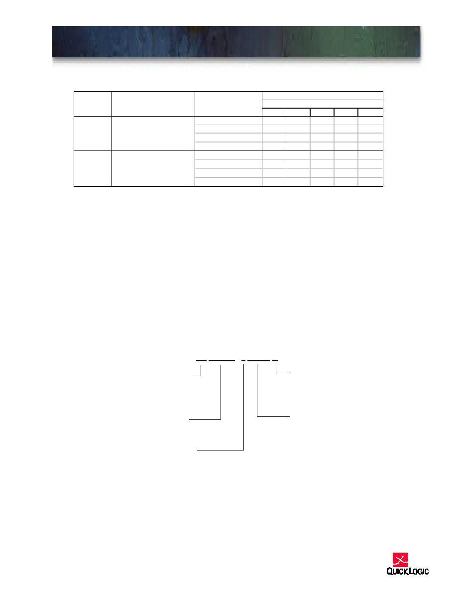
TABLE 1: Selector Table
D
EVICE
H
IGHLIGHTS
F
EATURES
Device
ASIC
Gates
PLD
Gates
Package
Max
I/O
Qualification
Level
SMD
5962-
QL8x12B
1,000
2,000
68CPGA
64
M
QL12x16B
2,000
4,000
84CPGA
76
M, /883
96836
144CPGA
122
M, /883
95599
QL16x24B
4,000
7,000
160 CQFP
122
M, /883
95599
208CQFP
180
M, /883
96837
QL24x32B
8,000
14,000
208PQFP
180
M
M = Military Temperature (-55 to +125 degrees C)
/883 = MIL-STD-883 qualified
8
Preliminary
8-8
Military 5.0V pASIC 1 Family
Product Summary
The pASIC 1 Family is a very-high-speed CMOS
user-programmable ASIC devices. The 768 logic cell
field-programmable gate array (FPGA) features
22,000 usable PLD gates of high-performance gen-
eral-purpose logic in a 208-pin PQFP and CQFP
package.
Low-impedance, metal-to-metal, ViaLink intercon-
nect technology provides nonvolatile custom logic
capable of operating above 150 MHz. Logic cell
delays under 2 ns, combined with input delays of
under 1.5 ns and output delays under 3 ns, permit
high-density programmable devices to be used with
today's fastest microprocessors and DSPs.
Designs can be entered using QuickLogic's Quick-
Works Toolkit or most popular third-party CAE tools.
QuickWorks combines Verilog/VHDL design entry
and simulation tools with device-specific place &
route and programming software. Ample on-chip
routing channels allow fast, fully automatic place and
route of designs using up to 100% of the logic and I/
O cells, while maintaining fixed pin-outs.
Pinout Diagram 68-Pin CPGA
TABLE 2: CPGA 68 Function/Connector Pin Table
P
RODUCT
S
UMMARY
P
INOUT
D
IAGRAM
68-P
IN
CPGA
PIN
FUNC
PIN
FUNC
PIN
FUNC
PIN
FUNC
B10
IO
B2
IO
K2
IO
K10
IO
A10
IO
B1
IO
L2
IO
K11
IO
B9
IO
C2
IO
K3
IO
J10
IO
A9
IO
C1
IO
L3
IO
J11
IO
B8
IO
D2
IO
K4
IO
H10
IO
A8
IO
D1
IO
L4
IO
H11
IO
B7
I/(SCLK)
E2
IO
K5
I/(SI)
G10
IO
A7
I/CLK/(SM)
E1
IO
L5
I/CLK
G11
IO
B6
VCC
F2
GND
K6
VCC
F10
GND
A6
I
F1
IO
L6
I
F11
IO
B5
I
G2
IO
K7
I/(SO)
E10
IO
A5
IO
G1
IO
L7
IO
E11
IO
B4
IO
H2
IO
K8
IO
D10
IO
A4
IO
H1
IO
L8
IO
D11
IO
B3
IO
J2
IO
K9
IO
C10
IO
A3
IO
J1
IO
L9
IO
C11
IO
A2
IO
K1
IO
L10
IO
B11
IO
8-9
Military 5.0V pASIC 1 Family
Pinout Diagram 84-pin CPGA
TABLE 3: CPGA 84 Function/Connector Pin Table
P
INOUT
D
IAGRAM
84-P
IN
CPGA
PIN
FUNC
PIN
FUNC
PIN
FUNC
PIN
FUNC
B10
IO
B2
IO
K2
IO
K10
IO
B9
IO
C2
IO
K3
IO
J10
IO
A10
IO
B1
IO
L2
IO
K11
IO
A9
IO
C1
IO
L3
IO
J11
IO
B8
IO
D2
IO
K4
IO
H10
IO
A8
IO
D1
IO
L4
IO
H11
IO
A7
IO
E1
IO
L5
IO
G11
IO
C7
GND
E3
GND
J5
GND
G9
GND
A6
IO
E2
IO
L6
IO
G10
IO
B7
I/(SCLK)
F1
IO
K5
I/(SI)
F11
IO
C6
I/CLK/(SM)
F2
IO
J6
I/CLK
F10
IO
B6
I(P)
F3
IO
K6
I
F9
IO
B5
I
G1
IO
K7
I/(SO)
E11
IO
C5
VCC
G3
VCC
J7
VCC
E9
VCC
A5
IO
G2
IO
L7
IO
E10
IO
A4
IO
H1
IO
L8
IO
D11
IO
B4
IO
H2
IO
K8
IO
D10
IO
A3
IO
J1
IO
L9
IO
C11
IO
A2
IO
K1
IO
L10
IO
B11
IO
B3
IO
J2
IO
K9
IO
C10
IO
A1
IO
L1
IO
L11
IO
A11
IO
10
Preliminary
8-10
Military 5.0V pASIC 1 Family
Pinout Diagram 144-pin CPGA
TABLE 4: CPGA 144 Function/Connector Table
(Cont'd on next page)
P
INOUT
D
IAGRAM
144-P
IN
CPGA
PIN
FUNC
PIN
FUNC
PIN
FUNC
PIN
FUNC
A2
IO
B15
IO
R14
IO
P1
IO
B3
IO
C14
IO
P13
IO
N2
IO
C4
IO
D13
IO
N12
IO
M3
IO
A3
IO
C15
IO
R13
IO
N1
IO
B4
IO
D14
IO
P12
IO
M2
IO
A4
IO
E13
VCC
R12
IO
L3
VCC
C3
VCC
D15
IO
N13
VCC
M1
IO
B5
IO
E14
IO
P11
IO
L2
IO
A5
IO
E15
IO
R11
IO
L1
IO
C6
IO
F13
IO
N10
IO
K3
IO
B6
IO
F14
IO
P10
IO
K2
IO
A6
IO
F15
IO
R10
IO
K1
IO
A7
IO
G15
IO
R9
IO
J1
IO
B7
IO
C13
GND
P9
IO
N3
GND
C5
GND
G14
IO
N11
GND
J2
IO
A8
IO
H15
IO
R8
IO
H1
IO
B8
I/(SCLK)
H14
IO
P8
I/(SI)
H2
IO
C8
I/CLK/(SM)
G13
GND
N8
I/CLK
J3
GND
C7
VCC
H13
IO
N9
VCC
H3
IO
A9
I/(P)
J15
IO
R7
I
G1
IO
B9
I
J14
IO
P7
I/(SO)
G2
IO
C11
VCC
J13
VCC
N5
VCC
G3
VCC
A10
IO
K15
IO
R6
IO
F1
IO
A11
IO
L15
IO
R5
IO
E1
IO
B10
IO
K14
IO
P6
IO
F2
IO
8-11
Military 5.0V pASIC 1 Family
CPGA 144 Function/Connector Table (Cont'd)
A12
IO
M15
IO
R4
IO
D1
IO
B11
IO
L14
IO
P5
IO
E2
IO
C10
IO
K13
IO
N6
IO
F3
IO
A13
IO
N15
IO
R3
IO
C1
IO
C9
GND
L13
GND
N7
GND
E3
GND
B12
IO
M14
IO
P4
IO
D2
IO
A14
IO
P15
IO
R2
IO
B1
IO
B13
IO
N14
IO
P3
IO
C2
IO
C12
IO
M13
IO
N4
IO
D3
IO
A15
IO
R15
IO
R1
IO
A1
IO
B14
IO
P14
nc
P2
IO
B2
nc
P
INOUT
D
IAGRAM
160-P
IN
CPGA
QL16x24B-1CF160M
12
Preliminary
8-12
Military 5.0V pASIC 1 Family
Pinout Diagram 208-pin CPGA
P
INOUT
D
IAGRAM
208-P
IN
CPGA
QL24X32B-1PQ208M
pASIC
Pin #1
Pin #157
Pin #53
Pin #105
8-13
Military 5.0V pASIC 1 Family
PQFP/CQFP 208 Function/Connector Table
PQFP/CQFP 208
F
UNCTION
/
CONNECTOR
T
ABLE
PIN
FUN
PIN
FUN
PIN
FUN
PIN
FUN
PIN
FUN
PIN
FUN
PIN
FUN
PIN
FUN
1
I/O
27
VCC
53
I/O
79
I/O
105
I/O
131
VCC
157
I/O
183
I/O
2
I/O
28
I/P
54
I/O
80
I/O
106
I/O
132
I
158
I/O
184
I/O
3
I/O
29
I
55
I/O
81
I/O
107
I/O
133
I/SO
159
I/O
185
I/O
4
I/O
30
VCC
56
I/O
82
I/O
108
I/O
134
VCC
160
I/O
186
I/O
5
I/O
31
I/O
57
I/O
83
VCC
109
I/O
135
I/O
161
I/O
187
VCC
6
I/O
32
I/O
58
I/O
84
I/O
110
I/O
136
I/O
162
I/O
188
I/O
7
I/O
33
I/O
59
GND
85
I/O
111
I/O
137
I/O
163
GND
189
I/O
8
I/O
34
I/O
60
I/O
86
I/O
112
I/O
138
I/O
164
I/O
190
I/O
9
I/O
35
I/O
61
VCC
87
I/O
113
I/O
139
I/O
165
VCC
191
I/O
10
VCC
36
I/O
62
I/O
88
I/O
114
VCC
140
I/O
166
I/O
192
I/O
11
I/O
37
I/O
63
I/O
89
I/O
115
I/O
141
I/O
167
I/O
193
I/O
12
GND
38
I/O
64
I/O
90
I/O
116
GND
142
I/O
168
I/O
194
I/O
13
I/O
39
I/O
65
I/O
91
I/O
117
I/O
143
I/O
169
I/O
195
I/O
14
I/O
40
I/O
66
I/O
92
I/O
118
I/O
144
I/O
170
I/O
196
I/O
15
I/O
41
VCC
67
I/O
93
I/O
119
I/O
145
VCC
171
I/O
197
I/O
16
I/O
42
I/O
68
I/O
94
I/O
120
I/O
146
I/O
172
I/O
198
I/O
17
I/O
43
GND
69
I/O
95
GND
121
I/O
147
GND
173
I/O
199
GND
18
I/O
44
I/O
70
I/O
96
I/O
122
I/O
148
I/O
174
I/O
200
I/O
19
I/O
45
I/O
71
I/O
97
VCC
123
I/O
149
I/O
175
I/O
201
VCC
20
I/O
46
I/O
72
I/O
98
I/O
124
I/O
150
I/O
176
I/O
202
I/O
21
I/O
47
I/O
73
GND
99
I/O
125
I/O
151
I/O
177
GND
203
I/O
22
I/O
48
I/O
74
I/O
100
I/O
126
I/O
152
I/O
178
I/O
204
I/O
23
GND
49
I/O
75
I/O
101
I/O
127
GND
153
I/O
179
I/O
205
I/O
24
I/O
50
I/O
76
I/O
102
I/O
128
I/O
154
I/O
180
I/O
206
I/O
25
I/Sck
51
I/O
77
I/O
103
I/O
129
I/SI
155
I/O
181
I/O
207
I/O
26
I/Clk
52
I/O
78
GND
104
I/O
130
I/Clk
156
I/O
182
GND
208
I/O

14
Preliminary
8-14
Military 5.0V pASIC 1 Family
ABSOLUTE MAXIMUM RATINGS
Supply Voltage ........................-0.5 to 7.0V
Input Voltage................ -0.5 to VCC +0.5V
ESD Pad Protection
.................... �
2000V
DC Input Current
.......................�20 mA
Latch-up Immunity
.................. �200 mA
Storage Temperature .......-65
�
C to +150
�
C
Lead Temperature ...........................300
�
C
5 Volt OPERATING RANGE
DC CHARACTERISTICS over 5V operating range
Notes:
[1] Capacitance is sample tested only. CI = 20 pF max on I/(SI).
[2] Only one output at a time. Duration should not exceed 30 seconds.
[3] Maximum Icc for military grade is 20 mA. For AC conditions use the formula described in the databook,
Section 9 - Power vs Operating Frequency.
[4] Stated timing for worst case Propagation Delay over process variation at VCC = 5.0V and TA = 25
�C. Mul-
tiply by the appropriate Delay Factor, K, for speed grade, voltage and temperature settings as specified in the
Operating Range.
[5] These limits are derived from a representative selection of the slowest paths through the pASIC logic cell
including net delays. Worst case delay values for specific paths should be determined from timing analysis
of your particular design.
Symbol
Parameter
Military
Unit
Min
Max
VCC
Supply Voltage
4.5
5.5
V
TA
Ambient Temperature
-55
�
C
TC
Case Temperature
125
�
C
K
Delay Factor
-0 Speed Grade
0.39
1.82
-1 Speed Grade
0.39
1.56
Symbol
Parameter
Conditions
Min
Max
Unit
VIH
Input HIGH Voltage
2.0
V
VIL
Input LOW Voltage
0.8
V
IOH = -4 mA
3.7
V
VOH
Output HIGH Voltage
IOH = 16 mA
2.4
V
IOH = -10
�
A
VCC-0.1
V
VOL
Output LOW Voltage
IOL = 8 mA
0.4
V
IOL = 10
�
A
0.1
V
II
Input Leakage Current
VI = VCC or GND
-10
10
�
A
IOZ
3-State Output Leakage Current
VI = VCC or GND
-10
10
�
A
CI
Input Capacitance [1]
10
pF
IOS
Output Short Circuit Current [2]
VO = GND
-10
-90
mA
VO = VCC
40
160
mA
ICC
D.C. Supply Current [3]
VI, VIO = VCC or GND
20
mA
8-15
Military 5.0V pASIC 1 Family
QL8X12B
AC CHARACTERISTICS at VCC = 5V, TA = 25
�C (K = 1.00)
Logic Cell
Input Cells
Output Cell
Notes:
[6] See High Drive Buffer Table for more information.
[7] Clock buffer fanout refers to the maximum number of flip flops per half column. The number of half
columns used does not affect clock buffer delay.
[8] The following loads are used for tPXZ:
QL8
X
12B
Propagation Delays (ns)
Symbol
Parameter
Fanout
1
2
3
4
8
tPD
Combinatorial Delay [5]
1.7
2.1
2.6
3.0
4.8
tSU
Setup Time [5]
2.1
2.1
2.1
2.1
2.1
tH
Hold Time
0.0
0.0
0.0
0.0
0.0
tCLK
Clock to Q Delay
1.0
1.5
1.9
2.3
4.2
tCWHI
Clock High Time
2.0
2.0
2.0
2.0
2.0
tCWLO
Clock Low Time
2.0
2.0
2.0
2.0
2.0
tSET
Set Delay
1.7
2.1
2.6
3.0
4.8
tRESET
Reset Delay
1.5
1.8
2.2
2.5
3.9
tSW
Set Width
1.9
1.9
1.9
1.9
1.9
tRW
Reset Width
1.8
1.8
1.8
1.8
1.8
Symbol
Parameter
Propagation Delays (ns) [4]
1
2
3
4
6
8
tIN
High Drive Input Delay [6]
2.1
2.2
2.3
2.4
2.6
2.9
tINI
High Drive Input, Inverting Delay [6]
2.1
2.2
2.3
2.5
2.8
3.1
tIO
Input Delay (bidirectional pad)
1.4
1.8
2.2
2.6
3.4
4.2
tGCK
Clock Buffer Delay [7]
2.7
2.7
2.8
2.9
3.0
tGCKHI
Clock Buffer Min High [7]
2.0
2.0
2.0
2.0
2.0
tGCKLO
Clock Buffer Min Low [7]
2.0
2.0
2.0
2.0
2.0
Propagation Delays (ns) [4]
Symbol
Parameter
Output Load Capacitance (pF)
30
50
75
100
150
tOUTLH
Output Delay Low to High
2.7
3.4
4.2
5.0
6.7
tOUTHL
Output Delay High to Low
2.8
3.7
4.7
5.6
7.6
tPZH
Output Delay Tri-state to High
4.0
4.9
6.1
7.3
9.7
tPZL
Output Delay Tri-state to Low
3.6
4.2
5.0
5.8
7.3
tPHZ
Output Delay High to Tri-state [8]
2.9
tPLZ
Output Delay Low to Tri-state [8]
3.3
16
Preliminary
8-16
Military 5.0V pASIC 1 Family
High Drive Buffer
[4] Stated timing for worst case Propagation Delay over process variation at VCC = 5.0V and TA = 25
�C.
Multiply by the appropriate Delay Factor, K, for speed grade, voltage and temperature settings as
specified in the Operating Range.
Clock Drivers
Propagation Delays (ns) [4]
Symbol
Parameter
Wired Together
Fanout
12
24
48
72
96
1
4.0
4.9
tIN
High Drive Input Delay
2
3.5
5.0
3
4.0
4.8
5.6
4
4.1
4.8
1
4.2
5.1
tINI
High Drive Input,
2
3.7
5.2
Inverting Delay
3
4.2
5.0
5.8
4
4.3
5.0

8-17
Military 5.0V pASIC 1 Family
QL12x16B
AC CHARACTERISTICS at VCC = 5V, TA = 25
�C (K = 1.00)
Logic Cell
Input Cells
Output Cell
Notes:
[6] See High Drive Buffer Table for more information.
[7] Clock buffer fanout refers to the maximum number of flip flops per half column. The number of half col-
umns used does not affect clock buffer delay.
[8] The following loads are used for tPXZ:
QL12
X
16B
Propagation Delays (ns)
Symbol
Parameter
Fanout
1
2
3
4
8
tPD
Combinatorial Delay [5]
1.7
2.2
2.6
3.2
5.2
tSU
Setup Time [5]
2.1
2.1
2.1
2.1
2.1
tH
Hold Time
0.0
0.0
0.0
0.0
0.0
tCLK
Clock to Q Delay
1.0
1.5
1.9
2.5
4.6
tCWHI
Clock High Time
2.0
2.0
2.0
2.0
2.0
tCWLO
Clock Low Time
2.0
2.0
2.0
2.0
2.0
tSET
Set Delay
1.7
2.1
2.6
3.2
5.2
tRESET
Reset Delay
1.5
1.9
2.2
2.7
4.3
tSW
Set Width
1.9
1.9
1.9
1.9
1.9
tRW
Reset Width
1.8
1.8
1.8
1.8
1.8
Symbol
Parameter
Propagation Delays (ns) [4]
1
2
3
4
6
8
tIN
High Drive Input Delay [6]
2.4
2.5
2.6
2.7
3.0
3.3
tINI
High Drive Input, Inverting Delay [6]
2.5
2.6
2.7
2.8
3.1
3.4
tIO
Input Delay (bidirectional pad)
1.4
1.9
2.2
2.8
3.7
4.6
tGCK
Clock Buffer Delay [7]
2.7
2.8
2.8
2.9
2.9
3.0
tGCKHI
Clock Buffer Min High [7]
2.0
2.0
2.0
2.0
2.0
2.0
tGCKLO
Clock Buffer Min Low [7]
2.0
2.0
2.0
2.0
2.0
2.0
Propagation Delays (ns) [4]
Symbol
Parameter
Output Load Capacitance (pF)
30
50
75
100
150
tOUTLH
Output Delay Low to High
2.7
3.4
4.2
5.0
6.7
tOUTHL
Output Delay High to Low
2.8
3.7
4.7
5.6
7.6
tPZH
Output Delay Tri-state to High
4.0
4.9
6.1
7.3
9.7
tPZL
Output Delay Tri-state to Low
3.6
4.2
5.0
5.8
7.3
tPHZ
Output Delay High to Tri-state [8]
2.9
tPLZ
Output Delay Low to Tri-state [8]
3.3

18
Preliminary
8-18
Military 5.0V pASIC 1 Family
High Drive Buffer
[4] Stated timing for worst case Propagation Delay over process variation at VCC = 5.0V and TA = 25
�C.
Multiply by the appropriate Delay Factor, K, for speed grade, voltage and temperature settings as
specified in the Operating Range.
Clock Drivers
Propagation Delays (ns) [4]
Symbol
Parameter
Wired Together
Fanout
12
24
48
72
96
1
4.5
5.4
tIN
High Drive Input Delay
2
3.9
5.6
3
4.5
5.3
6.3
4
4.6
5.3
1
4.7
5.6
tINI
High Drive Input,
2
4.0
5.8
Inverting Delay
3
4.6
5.5
6.4
4
4.8
5.5
8-19
Military 5.0V pASIC 1 Family
QL16x24B
AC CHARACTERISTICS at VCC = 5V, TA = 25
�C (K = 1.00)
Logic Cell
Input Cells
Output Cell
Notes:
[6] See High Drive Buffer Table for more information.
[7] Clock buffer fanout refers to the maximum number of flip flops per half column. The number of half col-
umns used does not affect clock buffer delay.
[8] The following loads are used for tPXZ:
QL16
X
24B
Propagation Delays (ns)
Symbol
Parameter
Fanout
1
2
3
4
8
tPD
Combinatorial Delay [5]
1.7
2.2
2.6
3.2
5.3
tSU
Setup Time [5]
2.1
2.1
2.1
2.1
2.1
tH
Hold Time
0.0
0.0
0.0
0.0
0.0
tCLK
Clock to Q Delay
1.0
1.5
1.9
2.6
4.7
tCWHI
Clock High Time
2.0
2.0
2.0
2.0
2.0
tCWLO
Clock Low Time
2.0
2.0
2.0
2.0
2.0
tSET
Set Delay
1.7
2.2
2.6
3.2
5.3
tRESET
Reset Delay
1.5
1.9
2.2
2.7
4.4
tSW
Set Width
1.9
1.9
1.9
1.9
1.9
tRW
Reset Width
1.8
1.8
1.8
1.8
1.8
Symbol
Parameter
Propagation Delays (ns) [4]
1
2
3
4
6
8
tIN
High Drive Input Delay [6]
2.8
2.9
3.0
3.1
4.0
5.3
tINI
High Drive Input, Inverting Delay [6]
3.0
3.1
3.2
3.3
4.1
5.7
tIO
Input Delay (bidirectional pad)
1.4
1.9
2.2
2.9
4.7
6.5
tGCK
Clock Buffer Delay [7]
2.7
2.8
2.9
3.0
3.1
3.3
tGCKHI
Clock Buffer Min High [7]
2.0
2.0
2.0
2.0
2.0
2.0
tGCKLO
Clock Buffer Min Low [7]
2.0
2.0
2.0
2.0
2.0
2.0
Propagation Delays (ns) [4]
Symbol
Parameter
Output Load Capacitance (pF)
30
50
75
100
150
tOUTLH
Output Delay Low to High
2.7
3.4
4.2
5.0
6.7
tOUTHL
Output Delay High to Low
2.8
3.7
4.7
5.6
7.6
tPZH
Output Delay Tri-state to High
4.0
4.9
6.1
7.3
9.7
tPZL
Output Delay Tri-state to Low
3.6
4.2
5.0
5.8
7.3
tPHZ
Output Delay High to Tri-state [8]
2.9
tPLZ
Output Delay Low to Tri-state [8]
3.3
20
Preliminary
8-20
Military 5.0V pASIC 1 Family
High Drive Buffer
[4] Stated timing for worst case Propagation Delay over process variation at VCC = 5.0V and TA = 25
�C.
Multiply by the appropriate Delay Factor, K, for speed grade, voltage and temperature settings as spec-
ified in the Operating Range.
Clock Drivers
Propagation Delays (ns) [4]
Symbol
Parameter
Wired Together
Fanout
12
24
48
72
96
1
5.3
6.7
tIN
High Drive Input Delay
2
4.5
6.6
3
5.3
6.2
7.2
4
5.4
6.2
1
5.7
7.2
tINI
High Drive Input,
2
4.6
6.8
Inverting Delay
3
5.5
6.4
7.4
4
5.6
6.4
8-21
Military 5.0V pASIC 1 Family
QL24x32B
AC CHARACTERISTICS at VCC = 5V, TA = 25
�C (K = 1.00)
Logic Cell
Input Cells
Output Cell
Notes:
[6] See High Drive Buffer Table for more information.
[7] Clock buffer fanout refers to the maximum number of flip flops per half column. The number of
half columns used does not affect clock buffer delay.
[8] The following loads are used for tPXZ:
QL24
X
32B
Propagation Delays (ns)
Symbol
Parameter
Fanout
1
2
3
4
8
tPD
Combinatorial Delay [5]
1.7
2.1
2.7
3.3
5.5
tSU
Setup Time [5]
2.1
2.1
2.1
2.1
2.1
tH
Hold Time
0.0
0.0
0.0
0.0
0.0
tCLK
Clock to Q Delay
1.0
1.5
1.9
2.7
4.9
tCWHI
Clock High Time
2.0
2.0
2.0
2.0
2.0
tCWLO
Clock Low Time
2.0
2.0
2.0
2.0
2.0
tSET
Set Delay
1.7
2.2
2.7
3.3
5.5
tRESET
Reset Delay
1.5
1.9
2.3
2.8
4.6
tSW
Set Width
1.9
1.9
1.9
1.9
1.9
tRW
Reset Width
1.8
1.8
1.8
1.8
1.8
Symbol
Parameter
Propagation Delays (ns) [4]
1
2
3
4
8
12
16
tIN
High Drive Input Delay [6]
3.1
3.2
3.3
3.4
4.4
5.8
6.5
tINI
High Drive Input, Inverting Delay [6]
3.3
3.4
3.5
3.6
4.6
6.0
6.7
tIO
Input Delay (bidirectional pad)
1.4
1.9
2.3
3.0
4.8
6.7
8.5
tGCK
Clock Buffer Delay [7]
2.7
2.8
2.9
3.0
3.1
3.3
3.4
tGCKHI
Clock Buffer Min High [7]
2.0
2.0
2.0
2.0
2.0
2.0
2.0
tGCKLO
Clock Buffer Min Low [7]
2.0
2.0
2.0
2.0
2.0
2.0
2.0
Propagation Delays (ns) [4]
Symbol
Parameter
Output Load Capacitance (pF)
30
50
75
100
150
tOUTLH
Output Delay Low to High
2.7
3.3
3.8
4.3
5.4
tOUTHL
Output Delay High to Low
2.8
3.6
4.5
5.3
6.9
tPZH
Output Delay Tri-state to High
2.1
2.6
3.1
3.7
4.8
tPZL
Output Delay Tri-state to Low
2.6
3.3
4.1
4.9
6.5
tPHZ
Output Delay High to Tri-state [8]
2.9
tPLZ
Output Delay Low to Tri-state [8]
3.3
22
Preliminary
8-22
Military 5.0V pASIC 1 Family
High Drive Buffer
[4] Stated timing for worst case Propagation Delay over process variation at VCC = 5.0V and TA =
25
�C. Multiply by the appropriate Delay Factor, K, for speed grade, voltage and temperature set-
tings as specified in the Operating Range.
AC Performance
Propagation delays depend on routing, fanout, load
capacitance, supply voltage, junction temperature,
and process variation. The AC Characteristics are a
design guide to provide initial timing estimates at
nominal conditions. Worst case estimates are
obtained when nominal propagation delays are multi-
plied by the appropriate Delay Factor, K, as specified
in the Delay Factor table (Operating Range). The
effects of voltage and temperature variation are illus-
trated in the graphs on the following pages, K Factor
versus Voltage and Temperature. The pASIC Devel-
opment Tools incorporate data sheet AC Character-
istics into the QDIF database for pre-place-and-route
timing analysis. The SpDE Delay Modeler extracts
specific timing parameters for precise path analysis
or simulation results following place and route.
ORDERING INFORMATION
Clock Drivers
Propagation Delays (ns) [4]
Symbol
Parameter
Wired Together
Fanout
12
24
48
72
96
1
5.8
7.2
tIN
High Drive Input Delay
2
5.0
7.1
3
5.8
6.7
7.7
4
5.9
6.8
1
6.0
7.4
tINI
High Drive Input,
2
5.2
7.3
Inverting Delay
3
6.0
6.9
7.9
4
6.1
7.0
QL 24x32B - 1 CF208 M
QuickLogic
pASIC device
pASIC device part number
B = 0.65 micron CMOS
8x12B
12x16B
16x24B
24x32B
Operating Range
M = Military
M/883C = MIL STD 883
Package Code
CG68 = 68-pin CPGA
CG84 = 84-pin CPGA
CG144 = 144-pin CPGA
CF160 = 160-pin CQFD
PQ208 = 208-pin PQFP
CF208 = 208-pin CQFP
Speed Grade
0 = fast
1 = faster