 | –≠–ª–µ–∫—Ç—Ä–æ–Ω–Ω—ã–π –∫–æ–º–ø–æ–Ω–µ–Ω—Ç: QL3040 | –°–∫–∞—á–∞—Ç—å:  PDF PDF  ZIP ZIP |
8-23
60,000 Usable PLD Gate pASIC3 FPGA Combining High Performance and High Density
Military Plastic pASIC 3 Family
Rev B
Military pASIC 3 - 3.3V Family
Device Highlights
High Performance and High Density
s
60,000 Usable PLD Gates with 316 I/Os
s
16-bit counter speeds over 300 MHZ, data path
speeds over 400 MHz
s
0.35um four-layer metal non-volatile CMOS
process for smallest die sizes
Easy to Use/Fast Development Cycles
s
100% routable with 100% utilization and complete
pin-out stability
s
Variable-grain logic cells provide high performance
and 100% utilization
s
Comprehensive design tools include high quality
Verilog/VHDL synthesis
Advanced I/O Capabilities
s
Interfaces with both 3.3 volt and 5.0 volt devices
s
PCI compliant with 3.3V and 5.0V buses for -1/-2
speed grades
s
Full JTAG boundary scan
s
Registered I/O cells with individually controlled
clocks and output enables
Features
Total of 180 I/O pins
s
308 bidirectional input/output pins, PCI-compliant
for 5.0 volt and 3.3 volt buses for -1/-2 speed
grades
s
8 high-drive input/distributed network pins
Eight Low-Skew Distributed Networks
s
Two array clock/control networks available to the
logic cell flip-flop clock, set and reset inputs - each
driven by an input-only pin
s
Up to six global clock/control networks available
to the logic cell F1, clock, set and reset inputs and
the input and I/O register clock, reset and enable
inputs as well as the output enable control - each
driven by an input-only or I/O pin, or any logic cell
output or I/O cell feedback
High Performance
s
Input + logic cell + output total delays under 6 ns
s
Data path speeds exceeding 400 MHz
s
Counter speeds over 300 MHz
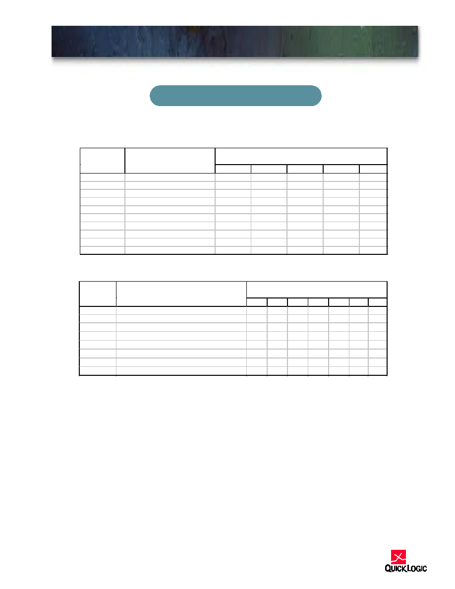
TABLE 1: Selector Table
D
EVICE
H
IGHLIGHTS
F
EATURES
Device
ASIC
Gates
PLD
Gates
Package
Max
I/O
Qualification
Level
Supply
Voltage
QL3012
8,000
12,000
84PLCC
68
M
3.3V
QL3025
16,000
25,000
208PQFP
174
M
3.3V
QL3040
24,000
40,000
208PQFP
174
M
3.3V
QL3060
36,000
60,000
208PQFP
174
M
3.3V
M = Military Temperature (-55 to +125 degrees C)
24
Preliminary
8-24
Military Plastic pASIC 3 Family
Product Summary
The pASIC 3 FPGA family features up to 60,000
usable PLD gates. pASIC 3 FPGAs are fabricated
on a 0.35mm four-layer metal process using Quick-
Logic's patented ViaLink technology to provide a
unique combination of high performance, high den-
sity, low cost, and extreme ease-of-use.
The pASIC 3 product family contains 1,584 logic
cells. With a maximum of 316 I/Os, and is available
in 208-PQFP and 84-PLCC packages.
Software support for the complete pASIC 3 family is
available through three basic packages. The turnkey
QuickWorks
Æ
package provides the most complete
FPGA software solution from design entry to logic
synthesis, to place and route, to simulation. The
QuickWorks
TM
-Lite and QuickTools
TM
packages pro-
vide a solution for designers who use Cadence,
Exemplar, Mentor, Synopsys, Synplicity, Viewlogic,
Veribest, or other third-party tools for design entry,
synthesis, or simulation.
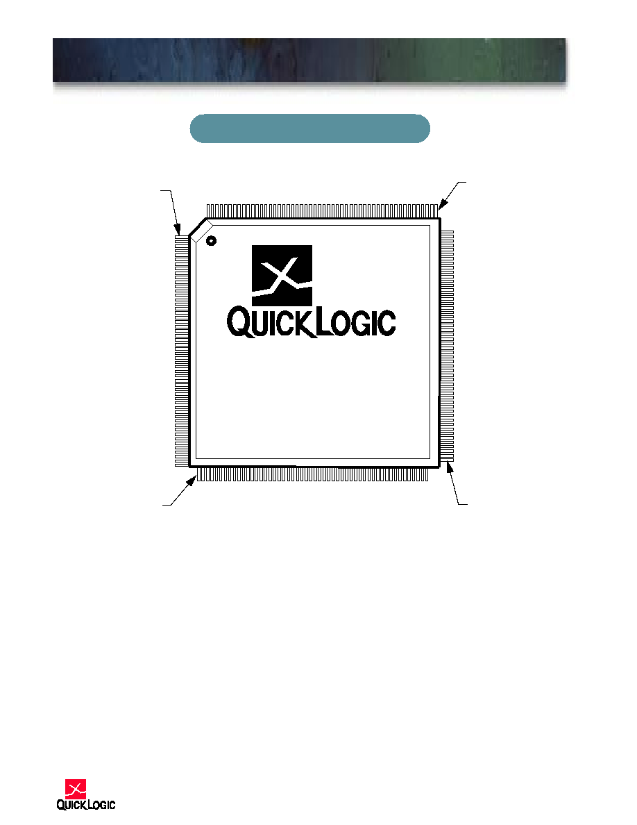
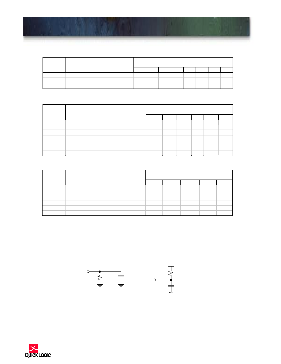
Pinout Diagram 68-Pin CPGA
TABLE 2: 84-pin PLCC
P
RODUCT
S
UMMARY
P
INOUT
D
IAGRAM
84-P
IN
PLCC
8-25
Military Plastic pASIC 3 Family
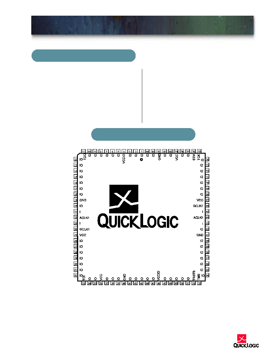
Pinout Diagram 208-Pin PQFP
QL3060-1PQ208M
pASIC
Pin #1
Pin #157
Pin #53
Pin #105
P
INOUT
D
IAGRAM
208-P
IN
PQFP

26
Preliminary
8-26
Military Plastic pASIC 3 Family
PQFP 208 Pinout Table
PQFP 208-P
INOUT
T
ABLE
208
Function
208
Function
208
Function
208
Function
208
Function
PQFP
PQFP
PQFP
PQFP
PQFP
208
I/O
43
GND
84
I/O
125
I/O
168
I/O
1
I/O
44
I/O
85
I/O
126
I/O
169
I/O
2
I/O
45
I/O
86
I/O
127
GND
NC
I/O
3
I/O
46
I/O
87
I/O
128
I/O
170
I/O
4
I/O
47
I/O
88
I/O
NC
I/O
171
I/O
5
I/O
48
I/O
89
I/O
129
GCLK / I
172
I/O
NC
I/O
NC
I/O
90
I/O
130
ACLK / I
173
I/O
6
I/O
49
I/O
91
I/O
131
VCC
174
I/O
7
I/O
50
I/O
92
I/O
132
GCLK / I
175
I/O
8
I/O
51
I/O
NC
I/O
133
GCLK / I
NC
I/O
9
I/O
52
I/O
93
I/O
134
VCC
176
I/O
10
VCC
53
I/O
94
I/O
135
I/O
177
GND
11
I/O
54
TDI
95
GND
136
I/O
178
I/O
12
GND
NC
I/O
96
I/O
NC
I/O
179
I/O
13
I/O
NC
I/O
97
VCC
137
I/O
NC
I/O
14
I/O
55
I/O
98
I/O
NC
GND
180
I/O
NC
I/O
56
I/O
99
I/O
138
I/O
181
I/O
15
I/O
NC
I/O
100
I/O
139
I/O
182
GND
16
I/O
57
I/O
NC
I/O
140
I/O
NC
VCC
17
I/O
58
I/O
101
I/O
141
I/O
183
I/O
18
I/O
59
GND
NC
I/O
142
I/O
184
I/O
19
I/O
60
I/O
102
I/O
NC
I/O
185
I/O
20
I/O
61
VCC
NC
I/O
143
I/O
186
I/O
NC
I/O
62
I/O
NC
I/O
144
I/O
187
VCCIO
21
I/O
63
I/O
103
TRSTB
145
VCC
188
I/O
22
I/O
64
I/O
104
TMS
NC
I/O
NC
I/O
23
GND
NC
I/O
105
I/O
146
I/O
189
I/O
24
I/O
65
I/O
NC
I/O
147
GND
190
I/O
25
GCLK / I
66
I/O
106
I/O
148
I/O
191
I/O
26
ACLK / I
67
I/O
107
I/O
149
I/O
192
I/O
27
VCC
NC
I/O
108
I/O
150
I/O
193
I/O
28
GCLK / I
68
I/O
109
I/O
151
I/O
194
I/O
29
GCLK / I
69
I/O
NC
I/O
152
I/O
NC
I/O
30
VCC
70
I/O
110
I/O
153
I/O
195
I/O
31
I/O
NC
I/O
111
I/O
154
I/O
196
I/O
32
I/O
71
I/O
112
I/O
155
I/O
197
I/O
NC
GND
NC
I/O
113
I/O
156
I/O
198
I/O
33
I/O
72
I/O
114
VCC
157
TCK
NC
I/O
NC
I/O
73
GND
115
I/O
158
STM
199
GND
34
I/O
74
I/O
116
GND
NC
I/O
200
I/O
35
I/O
NC
VCC
117
I/O
159
I/O
201
VCC
36
I/O
75
I/O
NC
I/O
160
I/O
202
I/O
NC
I/O
76
I/O
118
I/O
161
I/O
203
I/O
37
I/O
77
I/O
119
I/O
162
I/O
204
I/O
38
I/O
78
GND
120
I/O
163
GND
205
I/O
39
I/O
79
I/O
121
I/O
164
I/O
206
I/O
NC
I/O
80
I/O
NC
I/O
165
VCC
207
TDO
40
I/O
81
I/O
122
I/O
166
I/O
41
VCC
82
I/O
123
I/O
NC
I/O
42
I/O
83
VCCIO
124
I/O
167
I/O
8-27
Military Plastic pASIC 3 Family
ABSOLUTE MAXIMUM RATINGS
VCC Voltage ...........................-0.5 to 4.6V
VCCIO Voltage .......................-0.5 to 7.0V
Input Voltage.............. -0.5 to VCCIO+0.5V
Latch-up Immunity
.................. ±200 mA
DC Input Current
...................... ±20 mA
ESD Pad Protection
....................±
2000V
Storage Temperature .......-65
∞
C to +150
∞
C
Lead Temperature ...........................300
∞
C
OPERATING RANGE
DC CHARACTERISTICS
Notes:
[1] Military devices have 8 mA IOL specifications.
[2] Capacitance is sample tested only. Clock pins are 12 pF maximum.
[3] Only one output at a time. Duration should not exceed 30 seconds.
[4] Maximum ICC is 5 mA for all military grade devices. For AC conditions, contact QuickLogic
customer engineering.
Symbol
Parameter
Military
Unit
Min
Max
VCC
Supply Voltage
3.0
3.6
V
VCCIO
I/O Input Tolerance Voltage
3.0
5.5
V
TA
Ambient Temperature
-55
∞
C
TC
Case Temperature
125
∞
C
-0 Speed Grade
0.42
2.03
K
Delay Factor
-1 Speed Grade
0.42
1.64
-2 Speed Grade
0.42
1.37
Symbol
Parameter
Conditions
Min
Max
Unit
VIH
Input HIGH Voltage
0.5VCC VCCIO+0.5 V
VIL
Input LOW Voltage
-0.5
0.3VCC
V
VOH
Output HIGH Voltage
IOH = -12 mA
2.4
V
IOH = -500
µ
A
0.9VCC
V
VOL
Output LOW Voltage
IOL = 8 mA [1]
0.45
V
IOL = 1.5 mA
0.1VCC
V
II
I or I/O Input Leakage Current
VI = VCCIO or GND
-10
10
µ
A
IOZ
3-State Output Leakage Current
VI = VCCIO or GND
-10
10
µ
A
CI
Input Capacitance [2]
10
pF
IOS
Output Short Circuit Current [3]
VO = GND
-15
-180
mA
VO = VCC
40
210
mA
ICC
D.C. Supply Current [4]
VI, VIO = VCCIO or GND 0.50 (typ)
5
mA
ICCIO
D.C. Supply Current on VCCIO
0
100
µ
A
28
Preliminary
8-28
Military Plastic pASIC 3 Family
QL3012
AC CHARACTERISTICS at VCC = 3.3V, TA = 25
∞
C (K = 1.00)
(To calculate delays, multiply the appropriate K factor in the "Operating Range" section by the following numbers.)
Logic Cells
Input-Only/Clock Cells
Notes:
[5] Stated timing for worst case Propagation Delay over process variation at VCC=3.3V and TA=25
∞C.
Multiply by the appropriate Delay Factor, K, for speed grade, voltage and temperature settings as speci-
fied in the Operating Range.
[6] These limits are derived from a representative selection of the slowest paths through the pASIC 3 logic
cell including typical net delays. Worst case delay values for specific paths should be determined from
timing analysis of your particular design.
QL3012
Symbol
Parameter
Propagation Delays (ns)
Fanout [5]
1
2
3
4
8
tPD
Combinatorial Delay [6]
1.4
1.7
1.9
2.2
3.2
tSU
Setup Time [6]
1.7
1.7
1.7
1.7
1.7
tH
Hold Time
0.0
0.0
0.0
0.0
0.0
tCLK
Clock to Q Delay
0.7
1.0
1.2
1.5
2.5
tCWHI
Clock High Time
1.2
1.2
1.2
1.2
1.2
tCWLO
Clock Low Time
1.2
1.2
1.2
1.2
1.2
tSET
Set Delay
1.0
1.3
1.5
1.8
2.8
tRESET
Reset Delay
0.8
1.1
1.3
1.6
2.6
tSW
Set Width
1.9
1.9
1.9
1.9
1.9
tRW
Reset Width
1.8
1.8
1.8
1.8
1.8
Symbol
Parameter
Propagation Delays (ns)
Fanout [5]
1
2
3
4
8
12
24
tIN
High Drive Input Delay
1.5
1.6
1.8
1.9
2.4
2.9
4.4
tINI
High Drive Input, Inverting Delay
1.6
1.7
1.9
2.0
2.5
3.0
4.5
tISU
Input Register Set-Up Time
3.1
3.1
3.1
3.1
3.1
3.1
3.1
tIH
Input Register Hold Time
0.0
0.0
0.0
0.0
0.0
0.0
0.0
tlCLK
Input Register Clock To Q
0.7
0.8
1.0
1.1
1.6
2.1
3.6
tlRST
Input Register Reset Delay
0.6
0.7
0.9
1.0
1.5
2.0
3.5
tlESU
Input Register clock Enable Set-Up Time
2.3
2.3
2.3
2.3
2.3
2.3
2.3
tlEH
Input Register Clock Enable Hold Time
0.0
0.0
0.0
0.0
0.0
0.0
0.0

8-29
Military Plastic pASIC 3 Family
QL3012 Clock Cells
I/O Cells
Notes:
[7] The array distributed networks consist of 40 half columns and the global distributed networks consist of
44 half columns, each driven by an independent buffer. The number of half columns used does not
affect clock buffer delay. The array clock has up to 8 loads per half column. The global clock has up to
11 loads per half column.
[8] The following loads are used for tPXZ:
Symbol
Parameter
Propagation Delays (ns)
Loads per Half Column [7]
1
2
3
4
8
10
11
tACK
Array Clock Delay
1.2
1.2
1.3
1.3
1.5
1.6
1.7
tGCKP
Global Clock Pin Delay
0.7
0.7
0.7
0.7
0.7
0.7
0.7
tGCKB
Global Clock Buffer Delay
0.8
0.8
0.9
0.9
1.1
1.2
1.3
Symbol
Parameter
Propagation Delays (ns)
Fanout [5]
1
2
3
4
8
10
tI/O
Input Delay (bidirectional pad)
1.3
1.6
1.8
2.1
3.1
3.6
tISU
Input Register Set-Up Time
3.1
3.1
3.1
3.1
3.1
3.1
tIH
Input Register Hold Time
0.0
0.0
0.0
0.0
0.0
0.0
tlOCLK
Input Register Clock To Q
0.7
1.0
1.2
1.5
2.5
3.0
tlORST
Input Register Reset Delay
0.6
0.9
1.1
1.4
2.4
2.9
tlESU
Input Register clock Enable Set-Up Time
2.3
2.3
2.3
2.3
2.3
2.3
tlEH
Input Register Clock Enable Hold Time
0.0
0.0
0.0
0.0
0.0
0.0
Symbol
Parameter
Propagation Delays (ns)
Output Load Capacitance (pF)
30
50
75
100
150
tOUTLH
Output Delay Low to High
2.1
2.5
3.1
3.6
4.7
tOUTHL
Output Delay High to Low
2.2
2.6
3.2
3.7
4.8
tPZH
Output Delay Tri-state to High
1.2
1.7
2.2
2.8
3.9
tPZL
Output Delay Tri-state to Low
1.6
2.0
2.6
3.1
4.2
tPHZ
Output Delay High to Tri-State [8]
2.0
tPLZ
Output Delay Low to Tri-State [8]
1.2
5 pF
1K
5 pF
1K
tPHZ
tPLZ
30
Preliminary
8-30
Military Plastic pASIC 3 Family
QL3025
AC CHARACTERISTICS at VCC = 3.3V, TA = 25
∞
C (K = 1.00)
(To calculate delays, multiply the appropriate K factor in the "Operating Range" section by the following numbers.)
Logic Cells
Input-Only/Clock Cells
Notes:
[5] Stated timing for worst case Propagation Delay over process variation at VCC=3.3V and TA=25
∞C. Multi-
ply by the appropriate Delay Factor, K, for speed grade, voltage and temperature settings as specified in the
Operating Range.
[6] These limits are derived from a representative selection of the slowest paths through the pASIC 3 logic cell
including typical net delays. Worst case delay values for specific paths should be determined from timing
analysis of your particular design.
QL3025
Symbol
Parameter
Propagation Delays (ns)
Fanout [5]
1
2
3
4
8
tPD
Combinatorial Delay [6]
1.4
1.7
1.9
2.2
3.2
tSU
Setup Time [6]
1.7
1.7
1.7
1.7
1.7
tH
Hold Time
0.0
0.0
0.0
0.0
0.0
tCLK
Clock to Q Delay
0.7
1.0
1.2
1.5
2.5
tCWHI
Clock High Time
1.2
1.2
1.2
1.2
1.2
tCWLO
Clock Low Time
1.2
1.2
1.2
1.2
1.2
tSET
Set Delay
1.0
1.3
1.5
1.8
2.8
tRESET
Reset Delay
0.8
1.1
1.3
1.6
2.6
tSW
Set Width
1.9
1.9
1.9
1.9
1.9
tRW
Reset Width
1.8
1.8
1.8
1.8
1.8
Symbol
Parameter
Propagation Delays (ns)
Fanout [5]
1
2
3
4
8
12
24
tIN
High Drive Input Delay
1.5
1.6
1.8
1.9
2.4
2.9
4.4
tINI
High Drive Input, Inverting Delay
1.6
1.7
1.9
2.0
2.5
3.0
4.5
tISU
Input Register Set-Up Time
3.1
3.1
3.1
3.1
3.1
3.1
3.1
tIH
Input Register Hold Time
0.0
0.0
0.0
0.0
0.0
0.0
0.0
tlCLK
Input Register Clock To Q
0.7
0.8
1.0
1.1
1.6
2.1
3.6
tlRST
Input Register Reset Delay
0.6
0.7
0.9
1.0
1.5
2.0
3.5
tlESU
Input Register clock Enable Set-Up Time
2.3
2.3
2.3
2.3
2.3
2.3
2.3
tlEH
Input Register Clock Enable Hold Time
0.0
0.0
0.0
0.0
0.0
0.0
0.0
8-31
Military Plastic pASIC 3 Family
QL3025 Clock Cells
I/O Cells
Notes:
[7] The array distributed networks consist of 56 half columns and the global distributed networks consist of
60 half columns, each driven by an independent buffer. The number of half columns used does not
affect clock buffer delay. The array clock has up to 12 loads per half column. The global clock has up
to 15 loads per half column.
[8] The following loads are used for tPXZ:
Symbol
Parameter
Propagation Delays (ns)
Loads per Half Column [7]
1
2
3
4
8
10
12
15
tACK
Array Clock Delay
1.2
1.2
1.3
1.3
1.5
1.6
1.7
1.8
tGCKP
Global Clock Pin Delay
0.7
0.7
0.7
0.7
0.7
0.7
0.7
0.7
tGCKB
Global Clock Buffer Delay
0.8
0.8
0.9
0.9
1.1
1.2
1.3
1.4
Symbol
Parameter
Propagation Delays (ns)
Fanout [5]
1
2
3
4
8
10
tI/O
Input Delay (bidirectional pad)
1.3
1.6
1.8
2.1
3.1
3.6
tISU
Input Register Set-Up Time
3.1
3.1
3.1
3.1
3.1
3.1
tIH
Input Register Hold Time
0.0
0.0
0.0
0.0
0.0
0.0
tlOCLK
Input Register Clock To Q
0.7
1.0
1.2
1.5
2.5
3.0
tlORST
Input Register Reset Delay
0.6
0.9
1.1
1.4
2.4
2.9
tlESU
Input Register clock Enable Set-Up Time
2.3
2.3
2.3
2.3
2.3
2.3
tlEH
Input Register Clock Enable Hold Time
0.0
0.0
0.0
0.0
0.0
0.0
Symbol
Parameter
Propagation Delays (ns)
Output Load Capacitance (pF)
30
50
75
100
150
tOUTLH
Output Delay Low to High
2.1
2.5
3.1
3.6
4.7
tOUTHL
Output Delay High to Low
2.2
2.6
3.2
3.7
4.8
tPZH
Output Delay Tri-state to High
1.2
1.7
2.2
2.8
3.9
tPZL
Output Delay Tri-state to Low
1.6
2.0
2.6
3.1
4.2
tPHZ
Output Delay High to Tri-State [8]
2.0
tPLZ
Output Delay Low to Tri-State [8]
1.2
5 pF
1K
5 pF
1K
tPHZ
tPLZ
32
Preliminary
8-32
Military Plastic pASIC 3 Family
QL3040
AC CHARACTERISTICS at VCC = 3.3V, TA = 25
∞
C (K = 1.00)
(To calculate delays, multiply the appropriate K factor in the "Operating Range" section by the following numbers.)
Logic Cells
Input-Only/Clock Cells
Notes:
[5] Stated timing for worst case Propagation Delay over process variation at VCC=3.3V and TA=25
∞C.
Multiply by the appropriate Delay Factor, K, for speed grade, voltage and temperature settings as
specified in the Operating Range.
[6] These limits are derived from a representative selection of the slowest paths through the pASIC 3 logic
cell including typical net delays. Worst case delay values for specific paths should be determined from
timing analysis of your particular design.
QL3040
Symbol
Parameter
Propagation Delays (ns)
Fanout [5]
1
2
3
4
8
tPD
Combinatorial Delay [6]
1.4
1.7
1.9
2.2
3.2
tSU
Setup Time [6]
1.7
1.7
1.7
1.7
1.7
tH
Hold Time
0.0
0.0
0.0
0.0
0.0
tCLK
Clock to Q Delay
0.7
1.0
1.2
1.5
2.5
tCWHI
Clock High Time
1.2
1.2
1.2
1.2
1.2
tCWLO
Clock Low Time
1.2
1.2
1.2
1.2
1.2
tSET
Set Delay
1.0
1.3
1.5
1.8
2.8
tRESET
Reset Delay
0.8
1.1
1.3
1.6
2.6
tSW
Set Width
1.9
1.9
1.9
1.9
1.9
tRW
Reset Width
1.8
1.8
1.8
1.8
1.8
Symbol
Parameter
Propagation Delays (ns)
Fanout [5]
1
2
3
4
8
12
24
tIN
High Drive Input Delay
1.5
1.6
1.8
1.9
2.4
2.9
4.4
tINI
High Drive Input, Inverting Delay
1.6
1.7
1.9
2.0
2.5
3.0
4.5
tISU
Input Register Set-Up Time
3.1
3.1
3.1
3.1
3.1
3.1
3.1
tIH
Input Register Hold Time
0.0
0.0
0.0
0.0
0.0
0.0
0.0
tlCLK
Input Register Clock To Q
0.7
0.8
1.0
1.1
1.6
2.1
3.6
tlRST
Input Register Reset Delay
0.6
0.7
0.9
1.0
1.5
2.0
3.5
tlESU
Input Register clock Enable Set-Up Time
2.3
2.3
2.3
2.3
2.3
2.3
2.3
tlEH
Input Register Clock Enable Hold Time
0.0
0.0
0.0
0.0
0.0
0.0
0.0

8-33
Military Plastic pASIC 3 Family
QL3040 Clock Cells
I/O Cells
Notes:
[7] The array distributed networks consist of 72 half columns and the global distributed networks consist of
76 half columns, each driven by an independent buffer. The number of half columns used does not
affect clock buffer delay. The array clock has up to 14 loads per half column. The global clock has up
to 16 loads per half column.
[8] The following loads are used for tPXZ:
Symbol
Parameter
Propagation Delays (ns)
Loads per Half Column [7]
1
2
3
4
8
10
12
14
16
tACK
Array Clock Delay
1.2
1.2
1.3
1.3
1.5
1.6
1.7
1.8
1.9
tGCKP
Global Clock Pin Delay
0.7
0.7
0.7
0.7
0.7
0.7
0.7
0.7
0.7
tGCKB
Global Clock Buffer Delay
0.8
0.8
0.9
0.9
1.1
1.2
1.3
1.4
1.5
Symbol
Parameter
Propagation Delays (ns)
Fanout [5]
1
2
3
4
8
10
tI/O
Input Delay (bidirectional pad)
1.3
1.6
1.8
2.1
3.1
3.6
tISU
Input Register Set-Up Time
3.1
3.1
3.1
3.1
3.1
3.1
tIH
Input Register Hold Time
0.0
0.0
0.0
0.0
0.0
0.0
tlOCLK
Input Register Clock To Q
0.7
1.0
1.2
1.5
2.5
3.0
tlORST
Input Register Reset Delay
0.6
0.9
1.1
1.4
2.4
2.9
tlESU
Input Register clock Enable Set-Up Time
2.3
2.3
2.3
2.3
2.3
2.3
tlEH
Input Register Clock Enable Hold Time
0.0
0.0
0.0
0.0
0.0
0.0
Symbol
Parameter
Propagation Delays (ns)
Output Load Capacitance (pF)
30
50
75
100
150
tOUTLH
Output Delay Low to High
2.1
2.5
3.1
3.6
4.7
tOUTHL
Output Delay High to Low
2.2
2.6
3.2
3.7
4.8
tPZH
Output Delay Tri-state to High
1.2
1.7
2.2
2.8
3.9
tPZL
Output Delay Tri-state to Low
1.6
2.0
2.6
3.1
4.2
tPHZ
Output Delay High to Tri-State [8]
2.0
tPLZ
Output Delay Low to Tri-State [8]
1.2
5 pF
1K
5 pF
1K
tPHZ
tPLZ

34
Preliminary
8-34
Military Plastic pASIC 3 Family
QL3060
AC CHARACTERISTICS at VCC = 3.3V, TA = 25
∞
C (K = 1.00)
(To calculate delays, multiply the appropriate K factor in the "Operating Range" section by the following numbers.)
Logic Cells
Input-Only/Clock Cells
Notes:
[5] Stated timing for worst case Propagation Delay over process variation at VCC=3.3V and TA=25
∞C.
Multiply by the appropriate Delay Factor, K, for speed grade, voltage and temperature settings as
specified in the Operating Range.
[6] These limits are derived from a representative selection of the slowest paths through the pASIC 3
logic cell including typical net delays. Worst case delay values for specific paths should be deter-
mined from timing analysis of your particular design.
QL3060
Symbol
Parameter
Propagation Delays (ns)
Fanout [5]
1
2
3
4
8
tPD
Combinatorial Delay [6]
1.4
1.7
1.9
2.2
3.2
tSU
Setup Time [6]
1.7
1.7
1.7
1.7
1.7
tH
Hold Time
0.0
0.0
0.0
0.0
0.0
tCLK
Clock to Q Delay
0.7
1.0
1.2
1.5
2.5
tCWHI
Clock High Time
1.2
1.2
1.2
1.2
1.2
tCWLO
Clock Low Time
1.2
1.2
1.2
1.2
1.2
tSET
Set Delay
1.0
1.3
1.5
1.8
2.8
tRESET
Reset Delay
0.8
1.1
1.3
1.6
2.6
tSW
Set Width
1.9
1.9
1.9
1.9
1.9
tRW
Reset Width
1.8
1.8
1.8
1.8
1.8
Symbol
Parameter
Propagation Delays (ns)
Fanout [5]
1
2
3
4
8
12
24
tIN
High Drive Input Delay
1.5
1.6
1.8
1.9
2.4
2.9
4.4
tINI
High Drive Input, Inverting Delay
1.6
1.7
1.9
2.0
2.5
3.0
4.5
tISU
Input Register Set-Up Time
3.1
3.1
3.1
3.1
3.1
3.1
3.1
tIH
Input Register Hold Time
0.0
0.0
0.0
0.0
0.0
0.0
0.0
tlCLK
Input Register Clock To Q
0.7
0.8
1.0
1.1
1.6
2.1
3.6
tlRST
Input Register Reset Delay
0.6
0.7
0.9
1.0
1.5
2.0
3.5
tlESU
Input Register clock Enable Set-Up Time
2.3
2.3
2.3
2.3
2.3
2.3
2.3
tlEH
Input Register Clock Enable Hold Time
0.0
0.0
0.0
0.0
0.0
0.0
0.0
8-35
Military Plastic pASIC 3 Family
QL3060 Clock Cells
I/O Cells
Notes:
[7] The array distributed networks consist of 88 half columns and the global distributed networks
consist of 92 half columns, each driven by an independent buffer. The number of half columns
used does not affect clock buffer delay. The array clock has up to 18 loads per half column. The
global clock has up to 20 loads per half column.
[8] The following loads are used for tPXZ:
Symbol
Parameter
Propagation Delays (ns)
Loads per Half Column [7]
1
2
3
4
8
10
12
14
16
18
20
tACK
Array Clock Delay
1.2
1.2
1.3
1.3
1.5
1.6
1.7
1.8
1.9
2
2.1
tGCKP
Global Clock Pin Delay
0.7
0.7
0.7
0.7
0.7
0.7
0.7
0.7
0.7
0.7
0.7
tGCKB
Global Clock Buffer Delay
0.8
0.8
0.9
0.9
1.1
1.2
1.3
1.4
1.5
1.6
1.7
Symbol
Parameter
Propagation Delays (ns)
Fanout [5]
1
2
3
4
8
10
tI/O
Input Delay (bidirectional pad)
1.3
1.6
1.8
2.1
3.1
3.6
tISU
Input Register Set-Up Time
3.1
3.1
3.1
3.1
3.1
3.1
tIH
Input Register Hold Time
0.0
0.0
0.0
0.0
0.0
0.0
tlOCLK
Input Register Clock To Q
0.7
1.0
1.2
1.5
2.5
3.0
tlORST
Input Register Reset Delay
0.6
0.9
1.1
1.4
2.4
2.9
tlESU
Input Register clock Enable Set-Up Time
2.3
2.3
2.3
2.3
2.3
2.3
tlEH
Input Register Clock Enable Hold Time
0.0
0.0
0.0
0.0
0.0
0.0
Symbol
Parameter
Propagation Delays (ns)
Output Load Capacitance (pF)
30
50
75
100
150
tOUTLH
Output Delay Low to High
2.1
2.5
3.1
3.6
4.7
tOUTHL
Output Delay High to Low
2.2
2.6
3.2
3.7
4.8
tPZH
Output Delay Tri-state to High
1.2
1.7
2.2
2.8
3.9
tPZL
Output Delay Tri-state to Low
1.6
2.0
2.6
3.1
4.2
tPHZ
Output Delay High to Tri-State [8]
2.0
tPLZ
Output Delay Low to Tri-State [8]
1.2
5 pF
1K
5 pF
1K
tPHZ
tPLZ
36
Preliminary
8-36
Military Plastic pASIC 3 Family
Pin Descriptions
Ordering Information
Pin
Function
Description
TDI
Test Data In for JTAG
Hold HIGH during normal operation. Connect to
VCC if not used for JTAG.
TRSTB
Active low Reset for JTAG
Hold LOW during normal operation. Connect to
ground if not used for JTAG.
TMS
Test Mode Select for JTAG
Hold HIGH during normal operation. Connect to
VCC if not used for JTAG.
TCK
Test Clock for JTAG
Hold HIGH or LOW during normal operation.
Connect to VCC or ground if not used for JTAG.
TDO
Test data out for JTAG
Output that must be left unconnected if not used for
JTAG.
STM
Special Test Mode
Must be grounded during normal operation.
I/ACLK
High-drive input and/or
array network driver
Can be configured as either or both.
I/GCLK
High-drive input and/or
global network driver
Can be configured as either or both.
I
High-drive input
Use for input signals with high fanout.
I/O
Input/Output pin
Can be configured as an input and/or output.
VCC
Power supply pin
Connect to 3.3V supply.
VCCIO
Input voltage tolerance pin
Connect to 5.0 volt supply if 5 volt input tolerance is
required, otherwise connect to 3.3V supply.
GND
Ground pin
Connect to ground.
GND/THERM
Ground/Thermal pin
Available on 456-PBGA only. Connect to ground
plane on PCB if heat sinking desired. Otherwise
may be left unconnected.
QL 3060 ≠1 PQ208 M
Operating Range
M = Military
Package Code
PL84 = 84-pin PLCC
PQ208 = 208-pin PQFP
QuickLogic
pASIC device
pASIC 3 device
part number
3012
3025
3040
3060
Speed Grade
0 = quick
1 = fast
2 = faster