© 2002 QuickLogic Corporation
www.quicklogic.com
1
∑
∑
∑
∑
∑
∑
∑ ∑ ∑ ∑ ∑ ∑
Device Highlights
High Performance & High Density
∑
9,000 Usable PLD Gates with 82 I/Os
∑
300 MHz 16-bit Counters, 400 MHz
Datapaths, 160+ MHz FIFOs
∑
0.35
µ
m four-layer metal non-volatile
CMOS process for smallest die sizes
High Speed Embedded SRAM
∑
8 dual-port RAM modules, organized in
user-configurable 1,152 bit blocks
∑
5 ns access times, each port independently
accessible
∑
Fast and efficient for FIFO, RAM, and ROM
functions
Easy to Use / Fast Development
Cycles
∑
100% routable with 100% utilization and
complete pin-out stability
∑
Variable-grain logic cells provide high
performance and 100% utilization
∑
Comprehensive design tools include high
quality Verilog/VHDL synthesis
Advanced I/O Capabilities
∑
Interfaces with both 3.3 V and 5.0 V devices
∑
PCI compliant with 3.3 V and 5.0 V busses
for -1/-2/-3/-4 speed grades
∑
Full JTAG boundary scan
∑
I/O Cells with individually controlled
Registered Input Path and Output Enables
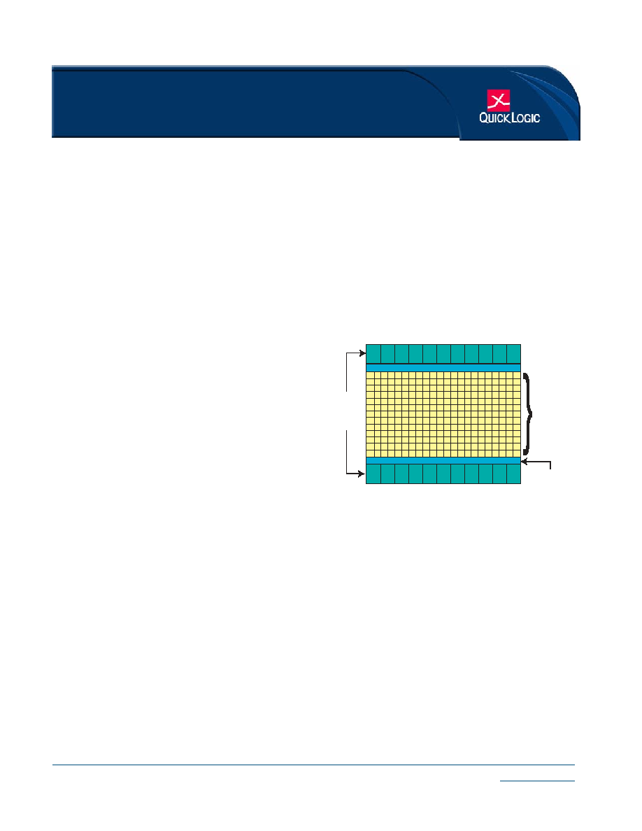
Figure 1: QuickRAM Block Diagram
8
RAM
Blocks
160
High Speed
Logic Cells
Interface
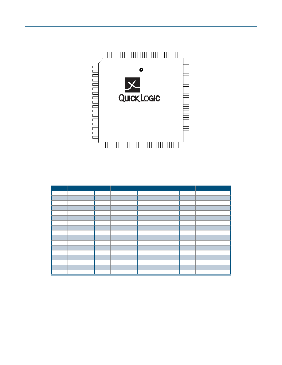
QL4009 QuickRAM Data Sheet
9,000 Usable PLD Gate QuickRAM ESP Combining Performance,
Density and Embedded RAM

2
www.quicklogic.com
© 2002 QuickLogic Corporation
∑
∑
∑
∑
∑
∑
QL4009 QuickRAM Data Sheet Rev B
Architecture Overview
The QuickRAM
TM
family of ESPs (Embedded Standard Products) offers FPGA logic in
combination with Dual-Port SRAM modules. The QL4009 is a 9,000 usable PLD gate
member of the QuickRAM family of ESPs. QuickRAM ESPs are fabricated on a 0.35
µ
m
four-layer metal process using QuickLogic's patented ViaLink
TM
technology to provide a
unique combination of high performance, high density, low cost, and extreme ease-of-use.
The QL4009 contains 160 logic cells and 8 Dual Port RAM modules (see
Figure 1
). Each
RAM module has 1,152 RAM bits, for a total of 9,216 bits. RAM Modules are Dual Port
(one read port, one write port) and can be configured into one of four modes: 64 (deep) x18
(wide), 128x9, 256x4, or 512x2 (see
Figure 4
). With a maximum of 82 I/Os, the QL4009
is available in 68-pin PLCC, 84-pin PLCC and 100-pin TQFP packages.
Designers can cascade multiple RAM modules to increase the depth or width allowed in
single modules by connecting corresponding address lines together and dividing the words
between modules (see
Figure 2
). This approach allows up to 512-deep configurations as
large as 16 bits wide in the smallest QuickRAM device and 44 bits wide in the largest device.
Software support for the complete QuickRAM family, including the QL4009, is available
through two basic packages. The turnkey QuickWorks
TM
package provides the most
complete ESP software solution from design entry to logic synthesis, to place and route, to
simulation. The QuickTools
TM
packages provides a solution for designers who use Cadence,
Exemplar, Mentor, Synopsys, Synplicity, Viewlogic, Aldec, or other third-party tools for
design entry, synthesis, or simulation.
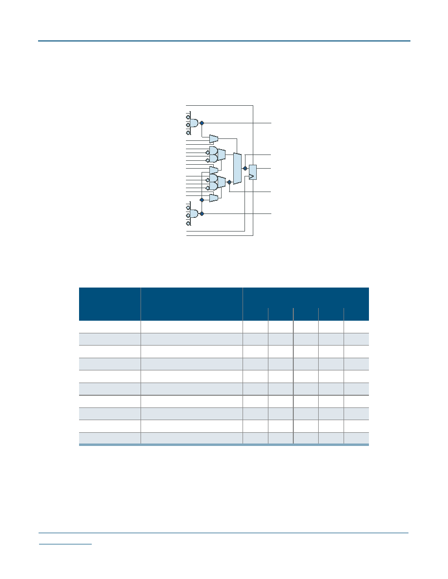
The QuickLogic variable grain logic cell features up to 16 simultaneous inputs and 5 outputs
within a cell that can be fragmented into 5 independent cells. Each cell has a fan-in of 29
including register and control lines (see
Figure 3
).
Figure 2: QuickRAM Module Bits
RDATA
WDATA
RADDR
RDATA
WADDR
WDATA
RAM
Module
(1,152 bits)
RAM
Module
(1,152 bits)

© 2002 QuickLogic Corporation
www.quicklogic.com
3
∑
∑
∑
∑
∑
∑
QL4009 QuickRAM Data Sheet Rev B
Product Summary
Total of 82 I/O Pins
∑
74 bi-directional input/output pins, PCI-compliant for 5.0 V and 3.3 V buses for
-1/-2/-3/-4 speed grades
∑
8 high-drive input/distributed network pins
Eight Low-Skew Distributed Networks
∑
Two array clock/control networks available to the logic cell flip-flop clock, set and reset
inputs - each driven by an input-only pin
∑
Six global clock/control networks available to the logic cell F1, clock, set and reset inputs
and the input and I/O register clock, reset and enable inputs as well as the output enable
control - each driven by an input-only or I/O pin, or any logic cell output or I/O cell
feedback
High Performance Silicon
∑
Input + logic cell + output total delays under 6 ns
∑
Data path speeds over 400 MHz
∑
Counter speeds over 300 MHz
∑
FIFO speeds over 160+ MHz
4
www.quicklogic.com
© 2002 QuickLogic Corporation
∑
∑
∑
∑
∑
∑
QL4009 QuickRAM Data Sheet Rev B
AC Characteristics at V
CC
= 3.3 V, T
A
= 25
∞
C (K = 1.00)
To calculate delays, multiply the appropriate K factor from
Table 10: Operating Range
by the
following numbers in the tables provided.
Figure 3: QuickRAM Logic Cell
Table 1: Logic Cell
Symbol
Parameter
Propagation Delays (ns)
Fanout (5)
1
2
3
4
5
t
PD
Combinatorial Delay
a
a. These limits are derived from a representative selection of the slowest paths through the Quick-
RAM logic cell including typical net delays. Worst case delay values for specific paths should be
determined from timing analysis of your particular design.
1.4
1.7
1.9
2.2
3.2
t
SU
Setup Time
a
1.7
1.7
1.7
1.7
1.7
t
H
Hold Time
0.0
0.0
0.0
0.0
0.0
t
CLK
Clock to Q Delay
0.7
1.0
1.2
1.5
2.5
t
CWHI
Clock High Time
1.2
1.2
1.2
1.2
1.2
t
CWLO
Clock Low Time
1.2
1.2
1.2
1.2
1.2
t
SET
Set Delay
1.0
1.3
1.5
1.8
2.8
t
RESET
Reset Delay
0.8
1.1
1.3
1.6
2.6
t
SW
Set Width
1.9
1.9
1.9
1.9
1.9
t
RW
Reset Width
1.8
1.8
1.8
1.8
1.8
QS
A1
A2
A3
A4
A5
A6
F1
F2
F3
F4
F5
F6
QS
OP
B1
B2
C1
C2
MP
MS
D1
D2
E1
E2
NP
NS
QC
QR
OZ
AZ
QZ
NZ
FZ

© 2002 QuickLogic Corporation
www.quicklogic.com
5
∑
∑
∑
∑
∑
∑
QL4009 QuickRAM Data Sheet Rev B
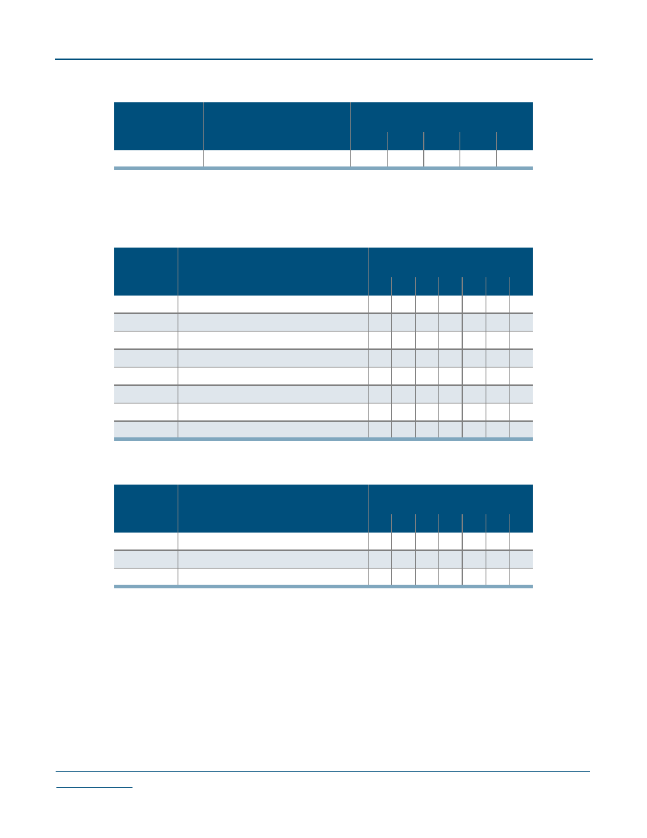
Figure 4: QuickRAM Module
Table 2: RAM Cell Synchronous Write Timing
Symbol
Parameter
Propagation Delays (ns)
Fanout
1
2
3
4
5
t
SWA
WA Setup Time to WCLK
1.0
1.0
1.0
1.0
1.0
t
HWA
WA Hold Time to WCLK
0.0
0.0
0.0
0.0
0.0
t
SWD
WD Setup Time to WCLK
1.0
1.0
1.0
1.0
1.0
t
HWD
WD Hold Time to WCLK
0.0
0.0
0.0
0.0
0.0
t
SWE
WE Setup Time to WCLK
1.0
1.0
1.0
1.0
1.0
t
HWE
WE Hold Time to WCLK
0.0
0.0
0.0
0.0
0.0
t
WCRD
WCLK to RD (WA=RA)
a
a. Stated timing for worst case Propagation Delay over process variation at V
CC
= 3.3 V and
T
A
= 25
∞
C. Multiply by the appropriate Delay Factor, K, for speed grade, voltage and temperature
settings as specified in the Operating Range.
5.0
5.3
5.6
5.9
7.1
Table 3: RAM Cell Synchronous Read Timing
Symbol
Parameter
Propagation Delays (ns)
Fanout
Logic Cells
1
2
3
4
5
t
SRA
RA Setup Time to RCLK
1.0
1.0
1.0
1.0
1.0
t
HRA
RA Hold Time to RCLK
0.0
0.0
0.0
0.0
0.0
t
SRE
RE Setup Time to RCLK
1.0
1.0
1.0
1.0
1.0
t
HRE
RE Hold Time to RCLK
0.0
0.0
0.0
0.0
0.0
t
RCRD
RCLK to RD
a
a. Stated timing for worst case Propagation Delay over process variation at V
CC
= 3.3 V and
TA = 25
∞
C. Multiply by the appropriate Delay Factor, K, for speed grade, voltage and temperature
settings as specified in the Operating Range.
4.0
4.3
4.6
4.9
6.1
WA
WD
WE
WCLK
RE
RCLK
RA
RD
[8:0]
[17:0]
[8:0]
[17:0]
MODE
ASYNCRD
[1:0]
6
www.quicklogic.com
© 2002 QuickLogic Corporation
∑
∑
∑
∑
∑
∑
QL4009 QuickRAM Data Sheet Rev B
Table 4: RAM Cell Asynchronous Read Timing
Symbol
Parameter
Propagation Delays (ns)
Fanout
1
2
3
4
5
RPDRD
RA to RD
a
a. Stated timing for worst case Propagation Delay over process variation at V
CC
= 3.3 V and
TA = 25
∞
C. Multiply by the appropriate Delay Factor, K, for speed grade, voltage and temperature
settings as specified in the Operating Range.
3.0
3.3
3.6
3.9
5.1
Table 5: Input-Only / Clock Cells
Symbol
Parameter
Propagation Delays (ns)
Fanout
1
2
3
4
8
12
24
t
IN
High Drive Input Delay
1.5
1.6
1.8
1.9
2.4
2.9
4.4
t
INI
High Drive Input, Inverting Delay
1.6
1.7
.19
2.0
2.5
3.0
4.5
t
ISU
Input Register Set-Up Time
3.1
3.1
3.1
3.1
3.1
3.1
3.1
t
IH
Input Register Hold Time
0.0
0.0
0.0
0.0
0.0
0.0
0.0
t
ICLK
Input Register Clock To Q
0.7
0.8
1.0
1.1
1.6
2.1
3.6
t
IRST
Input Register Reset Delay
0.6
0.7
0.9
1.0
1.5
2.0
3.5
t
IESU
Input Register Clock Enable Setup Time
2.3
2.3
2.3
2.3
2.3
2.3
2.3
t
IEH
Input Register Clock Enable Hold Time
0.0
0.0
0.0
0.0
0.0
0.0
0.0
Table 6: Clock Cells
Symbol
Parameter
Propagation Delays (ns)
Fanout
a
a. The array distributed networks consist of 40 half columns and the global distributed networks con-
sist of 44 half columns, each driven by an independent buffer. The number of half columns used
does not affect clock buffer delay. The array clock has up to 8 loads per half column. The global
clock has up to 11 loads per half column.
1
2
3
4
8
10
11
t
ACK
Array Clock Delay
1.2
1.2
1.3
1.3
1.5
1.6
1.7
t
GCKP
Global Clock Pin Delay
0.7
0.7
0.7
0.7
0.7
0.7
0.7
t
GCKB
Global Clock Buffer Delay
0.8
0.8
0.9
0.9
1.1
1.2
1.3
© 2002 QuickLogic Corporation
www.quicklogic.com
7
∑
∑
∑
∑
∑
∑
QL4009 QuickRAM Data Sheet Rev B
Table 7: I/O Cell Input Delays
Symbol
Parameter
Propagation Delays (ns)
Fanout
a
a. Stated timing for worst case Propagation Delay over process variation at V
CC
= 3.3 V and
T
A
= 25
∞
C. Multiply by the appropriate Delay Factor, K, for speed grade, voltage and temperature
settings as specified in the Operating Range.
1
2
3
4
8
10
t
I/O
Input Delay (bidirectional pad)
1.3
1.6
1.8
2.1
3.1
3.6
t
ISU
Input Register Set-Up Time
3.1
3.1
3.1
3.1
3.1
3.1
t
IH
Input Register Hold Time
0.0
0.0
0.0
0.0
0.0
0.0
t
IOCLK
Input Register Clock to Q
0.7
1.0
1.2
1.5
2.5
3.0
t
IORST
Input Register Reset Delay
0.6
0.9
1.1
1.4
2.4
2.9
t
IESU
Input Register Clock Enable Set-Up Time
2.3
2.3
2.3
2.3
2.3
2.3
t
IEH
Input Register Clock Enable Hold Time
0.0
0.0
0.0
0.0
0.0
0.0
Table 8: I/O Cell Output Delays
Symbol
Parameter
Propagation Delays (ns)
Output Load Capacitance (pF)
3
50
75
100
150
t
OUTLH
Output Delay Low to High
2.1
2.5
3.1
3.6
4.7
t
OUTHL
Output Delay High to Low
2.2
2.6
3.2
3.7
4.8
t
PZH
Output Delay Tri-state to High
1.2
1.7
2.2
2.8
3.9
t
PZL
Output Delay Tri-state to Low
1.6
2.0
2.6
3.1
4.2
t
PHZ
Output Delay High to Tri-state
a
a. The following loads are used for t
PXZ
2.0
-
-
-
-
t
PLZ
Output Delay High to Tri-state
a
1.2
-
-
-
-
1
1
tPHZ
tPLZ
5 pF
5 pF
8
www.quicklogic.com
© 2002 QuickLogic Corporation
∑
∑
∑
∑
∑
∑
QL4009 QuickRAM Data Sheet Rev B
DC Characteristics
The DC specifications are provided in the tables below.
Table 9: Absolute Maximum Ratings
Parameter
Value
Parameter
Value
V
CC
Voltage
-0.5 to 4.6 V
DC Input Current
±20 mA
V
CCIO
Voltage
-0.5 to 7.0 V
ESD Pad Protection
±2000V
Input Voltage
-0.5 V to V
CCIO
+0.5 V
Storage Temperature
-65∞ C to +150∞ C
Latch-up Immunity
±200 mA
Lead Temperature
300∞ C
Table 10: Operating Range
Symbol
Parameter
Military
Industrial
Commercial
Unit
Min
Max
Min
Max
Min
Max
V
CC
Supply Voltage
3.0
3.6
3.0
3.6
3.0
3.6
V
V
CCIO
I/O Input Tolerance Voltage
3.0
5.5
3.0
5.5
3.0
5.25
V
T
A
Ambient Temperature
-55
-
-40
85
0
70
∞ C
T
C
Case Temperature
-
125
-
-
-
-
∞ C
K
Delay Factor
-0 Speed Grade
0.42
2.03
0.43
1.90
0.46
1.85
n/a
-1 Speed Grade
0.42
1.64
0.43
1.54
0.46
1.50
n/a
-2 Speed Grade
0.42
1.37
0.43
1.28
0.46
1.25
n/a
-3 Speed Grade
0.43
0.90
0.46
0.88
n/a
-4 Speed Grade
0.43
0.82
0.46
0.80
n/a

© 2002 QuickLogic Corporation
www.quicklogic.com
9
∑
∑
∑
∑
∑
∑
QL4009 QuickRAM Data Sheet Rev B
Table 11: DC Characteristics
Symbol
Parameter
Conditions
Min
Max
Units
V
IH
Input HIGH Voltage
0.5V
CC
V
CCIO
+0.5
V
V
IL
Input LOW Voltage
-0.5
0.3V
CC
V
V
OH
Output HIGH Voltage
I
OH
= -12 mA
2.4
V
I
OH
= -500 µA
0.9V
CC
V
V
OL
Output LOW Voltage
I
OL
= 16 mA
a
a. Applies only to -1/-2/-3/-4 commercial grade devices. These speed grades are also PCI-compliant. All
other devices have 8 mA IOL specifications.
0.45
V
I
OL
= 1.5 mA
0.1V
CC
V
I
I
I or I/O Input Leakage Current
V
I
= V
CCIO
or GND
-10
10
µA
I
OZ
3-State Output Leakage Current
V
I
= V
CCIO
or GND
-10
10
µA
C
I
Input Capacitance
b
b. Capacitance is sample tested only. Clock pins are 12 pF maximum.
10
pF
I
OS
Output Short Circuit Current
c
c. Only one output at a time. Duration should not exceed 30 seconds.
V
O
= GND
-15
-180
mA
V
O
= V
CC
40
210
mA
I
CC
D.C. Supply Current
d
d. For -1/-2/-3/-4 commercial grade devices only. Maximum ICC is 3 mA for -0 commercial grade and all
industrial grade devices. and 5 mA for all military grade devices. For AC conditions, contact QuickLog-
ic customer applications group.
V
I
, V
IO
= V
CCIO
or GND
0.50 (typ)
2
mA
I
CCIO
D.C. Supply Current on V
CCIO
0
100
µA
10
www.quicklogic.com
© 2002 QuickLogic Corporation
∑
∑
∑
∑
∑
∑
QL4009 QuickRAM Data Sheet Rev B
Kv and Kt Graphs
Figure 5: Voltage Factor vs. Supply Voltage
Figure 6: Temperature Factor vs. Operating Temperature
0.9200
0.9400
0.9600
0.9800
1.0000
1.0200
1.0400
1.0600
1.0800
1.1000
3
3.1
3.2
3.3
3.4
3.5
3.6
Voltage Factor vs. Supply Voltage
Supply Voltage (V)
Kv
0.85
0.90
0.95
1.00
1.05
1.10
1.15
-60
-40
-20
0
20
40
60
80
Temperature Factor vs. Operating Temperature
Junction Temperature C
Kt
© 2002 QuickLogic Corporation
www.quicklogic.com
11
∑
∑
∑
∑
∑
∑
QL4009 QuickRAM Data Sheet Rev B
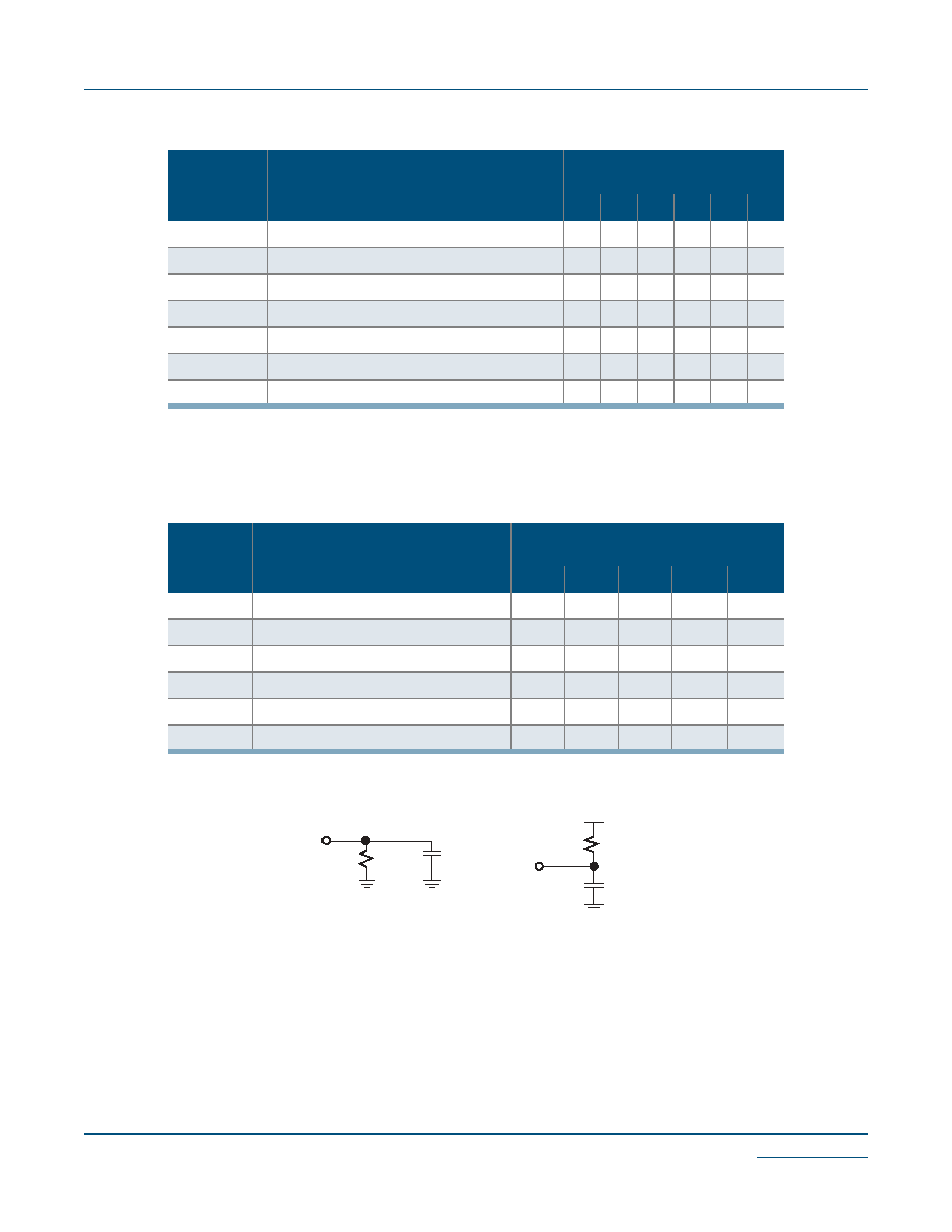
Power-up Sequencing
Figure 7: Power-up Requirements
The following requirements must be met when powering up the device:
(Refer to
Figure 7
above)
∑
When ramping up the power supplies keep (V
CCIO
-V
CC
)
MAX
500 mV. Deviation from
this recommendation can cause permanent damage to the device.
∑
V
CCIO
must lead V
CC
when ramping the device.
∑
The power supply must take greater than or equal to 400 µs to reach V
CC
. Ramping to
V
CC
/V
CCIO
earlier than 400 µs can cause the device to behave improperly.
An internal diode is present in-between V
CC
and V
CCIO
, as shown in
Figure 8
.
Figure 8: Internal Diode Between V
CC
and V
CCIO
Vol
t
age
V
CCIO
V
CC
(V
CCIO
-V
CC
)
MAX
Time
400 us
V
CC
V CC
V CCIO
Internal Logic
Cells, RAM
blocks, etc
IO Cells
12
www.quicklogic.com
© 2002 QuickLogic Corporation
∑
∑
∑
∑
∑
∑
QL4009 QuickRAM Data Sheet Rev B
JTAG
Figure 9: JTAG Block Diagram
Microprocessors and Application Specific Integrated Circuits (ASICs) pose many design
challenges, not the least of which concerns the accessibility of test points. The Joint Test
Access Group (JTAG) formed in response to this challenge, resulting in IEEE standard
1149.1, the Standard Test Access Port and Boundary Scan Architecture.
The JTAG boundary scan test methodology allows complete observation and control of the
boundary pins of a JTAG-compatible device through JTAG software. A Test Access Port
(TAP) controller works in concert with the Instruction Register (IR); these allow users to run
three required tests, along with several user-defined tests.
JTAG tests allow users to reduce system debug time, reuse test platforms and tools, and reuse
subsystem tests for fuller verification of higher level system elements.
TCK
TMS
TRSTB
RDI
TDO
Instruction Decode
&
Control Logic
TAp Controller
State Machine
(16 States)
Instruction Register
Boundary-Scan Register
(Data Register)
Mux
Bypass
Register
Mux
Internal
Register
I/O Registers
User Defined Data Register

© 2002 QuickLogic Corporation
www.quicklogic.com
13
∑
∑
∑
∑
∑
∑
QL4009 QuickRAM Data Sheet Rev B
The 1149.1 standard requires the following three tests:
∑
Extest Instruction.
The Extest instruction performs a PCB interconnect test. This test
places a device into an external boundary test mode, selecting the boundary scan
register to be connected between the TAP's Test Data In (TDI) and Test Data Out (TDO)
pins. Boundary scan cells are preloaded with test patterns (via the Sample/Preload
Instruction), and input boundary cells capture the input data for analysis.
∑
Sample/Preload Instruction.
This instruction allows a device to remain in its
functional mode, while selecting the boundary scan register to be connected between
the TDI and TDO pins. For this test, the boundary scan register can be accessed via a
data scan operation, allowing users to sample the functional data entering and leaving
the device.
∑
Bypass Instruction.
The Bypass instruction allows data to skip a device's boundary
scan entirely, so the data passes through the bypass register. The Bypass instruction
allows users to test a device without passing through other devices. The bypass register
is connected between the TDI and TDO pins, allowing serial data to be transferred
through a device without affecting the operation of the device.
14
www.quicklogic.com
© 2002 QuickLogic Corporation
∑
∑
∑
∑
∑
∑
QL4009 QuickRAM Data Sheet Rev B
Pin Descriptions
Ordering Information
Table 12: Pin Descriptions
Pin
Function
Description
TDI/RSI
Test Data In for JTAG /RAM init.
Serial Data In
Hold HIGH during normal operation. Connects to serial
PROM data in for RAM initialization. Connect to V
CC
if
unused.
TRSTB/RRO
Active low Reset for JTAG /RAM
init. reset out
Hold LOW during normal operation. Connects to serial
PROM reset for RAM initialization. Connect to GND if
unused.
TMS
Test Mode Select for JTAG
Hold HIGH during normal operation. Connect to V
CC
if
not used for JTAG.
TCK
Test Clock for JTAG
Hold HIGH or LOW during normal operation. Connect to
V
CC
or ground if not used for JTAG.
TDO/RCO
Test data out for JTAG /RAM init.
clock out
Connect to serial PROM clock for RAM initialization. Must
be left unconnected if not used for JTAG or RAM
initialization.
STM
Special Test Mode
Must be grounded during normal operation.
I/ACLK
High-drive input and/or array
network driver
Can be configured as either or both.
I/GCLK
High-drive input and/or global
network driver
Can be configured as either or both.
I
High-drive input
Use for input signals with high fanout.
I/O
Input/Output pin
Can be configured as an input and/or output.
V
CC
Power supply pin
Connect to 3.3 V supply.
V
CCIO
Input voltage tolerance pin
Connect to 5.0 V supply if 5 V input tolerance is required,
otherwise connect to 3.3 V supply.
GND
Ground pin
Connect to ground.
GND/THERM Ground/Thermal pin
Available on 456-PBGA only. Connect to ground plane on
PCB if heat sinking desired. Otherwise may be left
unconnected.
QL 4009 - 1 PF100 C
QuickLogic device
QuickRAM device
part number
Speed Grade
0 = Quick
1 = Fast
2 = Faster
3 = Faster
*4 = Wow
Operating Range
C = Commercial
I = Industrial
M = Military
Package Code
PL68 = 68-pin PLCC
PF84 = 84-pin PLCC
PF100 = 100-pin TQFP
* Contact QuickLogic regarding availabliity
© 2002 QuickLogic Corporation
www.quicklogic.com
15
∑
∑
∑
∑
∑
∑
QL4009 QuickRAM Data Sheet Rev B
68 PLCC Pinout Diagram
Figure 10: Top View of 68 Pin PLCC
68 PLCC Pinout Table
Table 13: 68 PLCC Pinout Table
68 PLCC
Function
68 PLCC
Function
68 PLCC
Function
68 PLCC
Function
1
GND
18
VCC
35
GND
52
VCC
2
I/O
19
GCLK/I
36
I/O
53
GCLK/I
3
I/O
20
GCLK/I
37
I/O
54
GCLK/I
4
VCCIO
21
I/O
38
I/O
55
I/O
5
I/O
22
I/O
39
VCCIO
56
I/O
6
I/O
23
I/O
40
I/O
57
I/O
7
I/O
24
I/O
41
I/O
58
I/O
8
I/O
25
I/O
42
TRSTB
58
I/O
9
TDO
26
I/O
43
TMS
60
I/O
10
I/O
27
TDI
44
I/O
61
TCK
11
I/O
28
I/O
45
I/O
62
STM
12
I/O
29
I/O
46
I/O
63
I/O
13
I/O
30
I/O
47
I/O
64
I/O
14
GND
31
I/O
48
GND
65
I/O
15
I/O
32
I/O
49
I/O
66
I/O
16
GCLK/I
33
I/O
50
GCLK/I
67
I/O
17
ACLK/I
34
I/O
51
ACLK/I
68
I/O
TDO
IO
IO
IO
IO
VCCIO
IO
IO
GND
IO
IO
IO
IO
IO
IO
STM
TCK IO
IO
IO
IO
IO
IO
GCLK/I
GCLK/I
VCC
ACLK/I
GCLK/I
IO
GND
IO
IO
IO
IO
TDI
IO
IO
IO
IO
IO
IO
IO
GND
IO
IO
IO
VCCIO
IO
IO
TRSTB
TMS
60
59
58
57
56
55
54
53
52
51
50
49
48
47
46
45
44
27 28 29 30 31 32 33 34 35 36 37 38 39 40 41 42 43
10
11
12
13
14
15
16
17
18
19
20
21
22
23
24
25
26
QL4009-1PL68C
QuickRAM
IO
IO
IO
IO
GND
IO
GCLK/I
ACLK/I
VCC
GCLK/I
GCLK/I
IO
IO
IO
IO
IO
IO
9 8 7 6 5 4 3 2 1 68 67 66 65 64 63 62 61

16
www.quicklogic.com
© 2002 QuickLogic Corporation
∑
∑
∑
∑
∑
∑
QL4009 QuickRAM Data Sheet Rev B
84 PLCC Pinout Diagram
Figure 11: Top View of 84 Pin PLCC
84 PLCC Pinout Table
Table 14: 84 PLCC Pinout Table
84 PLCC
Function
84 PLCC
Function
84 PLCC
Function
84 PLCC
Function
1
I/O
22
ACLK/I
43
I/O
64
ACLK/I
2
I/O
23
GCLK/I
44
I/O
65
GCLK/I
3
I/O
24
GCLK/I
45
I/O
66
GCLK/I
4
VCCIO
25
VCC
46
VCCIO
67
VCC
5
I/O
26
I/O
47
I/O
68
I/O
6
I/O
27
I/O
48
I/O
69
I/O
7
I/O
28
I/O
49
I/O
70
I/O
8
I/O
29
I/O
50
I/O
71
I/O
9
I/O
30
I/O
51
I/O
72
I/O
10
I/O
31
I/O
52
TRSTB
73
I/O
11
TDO
32
I/O
53
TMS
74
I/O
12
I/O
33
TDI
54
I/O
75
TCK
13
I/O
34
I/O
55
I/O
76
STM
14
I/O
35
I/O
56
I/O
77
I/O
15
I/O
36
VCC
57
I/O
78
I/O
16
I/O
37
I/O
58
I/O
79
VCC
17
I/O
38
I/O
59
I/O
80
I/O
18
I/O
39
I/O
60
I/O
81
I/O
19
GND
40
GND
61
GND
82
GND
20
I/O
41
I/O
62
I/O
83
I/O
21
GCLK/I
42
I/O
63
GCLK/I
84
I/O
TDO
IO
IO
IO
IO
IO
IO
VCCIO
IO
IO
IO
IO
IO
GND
IO
IO
VCC
IO
IO
STM
TCKIO
IO
IO
IO
IO
IO
IO
VCC
GCLK/I
GCLK/I
ACLK/I
GCLK/I
IO
GND
IO
IO
IO
IO
IO
IO
IO
TDI
IO
IO
VCC
IO
IO
IO
GND
IO
IO
IO
IO
IO
VCCIO
IO
IO
IO
IO
IO
TRSTB
TMS
74
73
72
71
70
69
68
67
66
65
64
63
62
61
60
59
58
57
56
55
54
33 34 35 36 37 38 39 40 41 42 43 44 45 46 47 48 49 50 51 52 53
12
13
14
15
16
17
18
19
20
21
22
23
24
25
26
27
28
29
30
31
32
QL4009-1PL84C
QuickRAM
IO
IO
IO
IO
IO
IO
IO
GND
IO
GCLK/I
ACLK/I
GCLK/I
GCLK/I
VCC
IO
IO
IO
IO
IO
IO
IO
11 10 9 8 7 6 5 4 3 2 1 84 83 82 81 80 79 78 77 76 75

© 2002 QuickLogic Corporation
www.quicklogic.com
17
∑
∑
∑
∑
∑
∑
QL4009 QuickRAM Data Sheet Rev B
100 TQFP Pinout Diagram
Figure 12: Top View of 100 Pin TQFP
100 TQFP Pinout Table
Table 15: 100 TQFP Pinout Table
100TQFP
Function
100TQFP
Function
100TQFP
Function
100TQFP
Function
1
I/O
26
TDI
51
I/O
76
TCK
2
I/O
27
I/O
52
I/O
77
STM
3
I/O
28
I/O
53
I/O
78
I/O
4
I/O
29
I/O
54
I/O
79
I/O
5
I/O
30
I/O
55
I/O
80
I/O
6
I/O
31
I/O
56
I/O
81
I/O
7
I/O
32
I/O
57
I/O
82
I/O
8
I/O
33
I/O
58
I/O
83
I/O
9
GND
34
I/O
59
GND
84
I/O
10
I/O
35
GND
60
I/O
85
GND
11
I
36
I/O
61
I
86
I/O
12
ACLK / I
37
I/O
62
ACLK / I
87
I/O
13
VCC
38
GND
63
VCC
88
GND
14
I
39
I/O
64
I
89
I/O
15
GCLK / I
40
I/O
65
GCLK / I
90
I/O
16
VCC
41
I/O
66
VCC
91
I/O
17
I/O
42
VCCIO
67
I/O
92
VCCIO
18
I/O
43
I/O
68
I/O
93
I/O
19
I/O
44
I/O
69
I/O
94
I/O
20
I/O
45
I/O
70
I/O
95
I/O
21
I/O
46
I/O
71
I/O
96
I/O
22
I/O
47
I/O
72
I/O
97
I/O
23
I/O
48
I/O
73
I/O
98
I/O
24
I/O
49
TRSTB
74
I/O
99
I/O
25
I/O
50
TMS
75
I/O
100
TDO
Pin 1
Pin 26
Pin 51
Pin 76
QL4009-1PF100C
QuickRAM

© 2002 QuickLogic Corporation
www.quicklogic.com
18
∑
∑
∑
∑
∑
∑
QL4009 QuickRAM Data Sheet Rev B
Contact Information
Telephone: 408 990 4000 (US)
416 497 8884 (Canada)
44 1932 57 9011 (Europe)
49 89 930 86 170 (Germany)
852 8106 9091 (Asia)
81 45 470 5525 (Japan)
E-mail:
info@quicklogic.com
Support:
support@quicklogic.com
Web site:
http://www.quicklogic.com/
Revision History
Copyright Information
Copyright © 2002 QuickLogic Corporation. All Rights Reserved.
The information contained in this product brief, and the accompanying software programs
are protected by copyright. All rights are reserved by QuickLogic Corporation. QuickLogic
Corporation reserves the right to make periodic modifications of this product without
obligation to notify any person or entity of such revision. Copying, duplicating, selling, or
otherwise distributing any part of this product without the prior written consent of an
authorized representative of QuickLogic is prohibited.
QuickLogic, pASIC, and ViaLink are registered trademarks, and SpDE and QuickWorks are
trademarks of QuickLogic Corporation.
Verilog is a registered trademark of Cadence Design Systems, Inc.
Table 16: Revision History
Revision
Date
Comments
A
5/2000
First release.
B
5/2002
Added Kfactor, Power-up, JTAG and mechanical
drawing information. Reformatted.