 | –≠–ª–µ–∫—Ç—Ä–æ–Ω–Ω—ã–π –∫–æ–º–ø–æ–Ω–µ–Ω—Ç: QT160 | –°–∫–∞—á–∞—Ç—å:  PDF PDF  ZIP ZIP |

l
Q
QProxTM QT160 / QT161
6 K
EY
C
HARGE
-T
RANSFER
QT
OUCH
TM S
ENSOR
IC
APPLICATIONS
Instrument panels
Gaming machines
Access systems
Pointing devices
Appliance controls
Security systems
PC Peripherals
Backlighted buttons
QT160 / QT161 charge-transfer ("QT'") QTouch ICs are self-contained digital controllers capable of detecting near-proximity or
touch from up to 6 electrodes. They allow electrodes to project 6 independent sense fields through any dielectric like glass,
plastic, stone, ceramic, and wood. They can also make metal-bearing objects responsive to proximity or touch by turning them
into intrinsic sensors. These capabilities coupled with continuous self-calibration can lead to entirely new product concepts,
adding high value to product designs.
Each of the 6 channels operate independently of the others, and each can be tuned for a unique sensitivity level by simply
changing its sample capacitor value.
The devices are designed specifically for human interfaces, like control panels, appliances, gaming devices, lighting controls,
or anywhere a mechanical switch or button may be found; they may also be used for some material sensing and control
applications. The option-selectable toggle mode permits on/off touch control, for example for light switch replacement.
The devices require only a common inexpensive capacitor per channel in order to function. The QT160 also offers the unique
adjacent key suppression (AKSTM, patent pending) feature which suppresses touch from weaker responding keys and allows
only a dominant key to detect, for example to solve the problem of large fingers on tightly spaced keys.
In most cases the power supply need only be minimally regulated, for example by an inexpensive 3-terminal regulator.
The RISC core of these devices employ signal processing techniques pioneered by Quantum; these are specifically designed
to make the device survive real-world challenges, such as `stuck sensor' conditions and signal drift.
By using the charge transfer principle, these parts deliver a level of performance clearly superior to older technologies yet are
highly cost-effective.
L
Q
Copyright © 2002 QRG Ltd
QT160/161 1.06/1102
6 completely independent touch circuits
Individual logic outputs per channel (active high)
Projects prox fields through any dielectric
Only one external capacitor required per channel
Sensitivity easily adjusted on a per-channel basis
100% autocal for life - no adjustments required
3-5.5V, 5mA single supply operation
Toggle mode for on/off control (strap option)
10s, 60s, infinite auto-recal timeout (strap options)
AKSTM Adjacent Key Suppression (QT160)
Less expensive per key than many mechanical switches
Eval board with backlighting - p/n E160
-
QT161-AS
-40
0
C to +105
0
C
QT161-D
-
0
0
C to +70
0
C
-
QT160-AS
-40
0
C to +105
0
C
QT160-D
-
0
0
C to +70
0
C
DIP-28
SSOP-28
T
A
AVAILABLE OPTIONS
NOTE: Pinouts are not the same!

1 - OVERVIEW
QT160/161 is a 6-channel burst mode digital charge-transfer
(QT) sensor designed specifically for touch controls; they
include all hardware and signal processing functions
necessary to provide stable sensing under a wide variety of
conditions. Only a single low cost, non-critical capacitor per
channel is required for operation.
Figure 1-1 shows the basic circuit using the device. See
Tables 7-1 and 7-2 (page 11) for pin listings. The DIP and
SOIC pinouts are not the same and serious damage can
occur if a part is mis-wired).
1.1 BASIC OPERATION
The devices employ bursts of charge-transfer cycles to
acquire signals. Burst mode permits low power operation,
dramatically reduces RF emissions, lowers susceptibility to
RF fields, and yet permits excellent speed. Internally, signals
are digitally processed to reject impulse noise using a
'consensus' filter that requires three consecutive
confirmations of detection. Each channel is measured in
sequence starting with channel 1.
The QT switches and charge measurement hardware
functions are all internal to the device (Figure 1-2). A 14-bit
single-slope switched capacitor ADC includes both the
required QT charge and transfer switches in a configuration
that provides direct ADC conversion. The ADC is designed
to dynamically optimize the QT burst length according to the
rate of charge buildup on Cs, which in turn depends on the
values of Cs, Cx, and Vdd. Vdd is used as the charge
reference voltage. Larger values of Cx cause the charge
transferred into Cs to rise more rapidly, reducing available
resolution; as a minimum resolution is required for proper
operation, this can result in dramatically reduced apparent
gain. Conversely, larger values of Cs reduce the rise of
differential voltage across it, increasing available resolution
by permitting longer QT bursts. The value of Cs can thus be
increased to allow larger values of Cx to be tolerated. The IC
is responsive to both Cx and Cs, and changes in Cs can
result in substantial changes in sensor gain.
Option pins allow the selection of several timing features.
1.2 ELECTRODE DRIVE
The devices have 6 independent channels. The internal ADC
treats Cs on each channel as a floating transfer capacitor; as
a direct result, the sense electrode can be connected to
either SNS1A or SN1B with no performance difference. In
both cases the rule Cs >> Cx must be observed for proper
operation. The polarity of the charge buildup across Cs
during a burst is the same in either case.
It is possible to connect separate Cx and Cx' loads to
SNS1A and SNS1B simultaneously, although the result is no
different than if the loads were connected together at SNS1A
(or SNS1B). It is important to limit the amount of stray
capacitance on both terminals, especially if the load Cx is
already large, for example by minimizing trace lengths and
widths so as not to exceed the Cx load specification and to
allow for a larger sensing electrode size if so desired.
Unused channels: If a channel is not used, a dummy
nominal 1nF sense capacitor of any type must be connected
to the SNS pins ensure correct operation.
The PCB traces, wiring, and any components associated
with or in contact with SNS1A and SNS1B will become touch
sensitive and should be treated with caution to limit the touch
area to the desired location. Multiple touch electrodes can be
used, for example to create a control button on both sides of
an object, however it is impossible for the sensor to
distinguish between the two touch areas.
1.3 KEY DESIGN
1.3.1 K
EY
G
EOMETRY
AND
S
IZE
There is no restriction on the shape of the key electrode; in
most cases common sense and a little experimentation can
result in a good electrode design. The devices will operate
equally well with long, thin keys as with round or square
ones; even random shapes are acceptable. The electrode
can also be a 3-dimensional surface or object. Sensitivity is
related to the amount of surface metallization, touch contact
area, overlying panel material and thickness, and ground
coupling quality of the sensor
circuit.
If a relatively large touch area is
desired, and if tests show that
the electrode has more
capacitance than the part can
tolerate, the electrode can be
made into a sparse mesh (Figure
1-3) having lower Cx than a solid
plane.
1.3.2 B
ACKLIGHTING
K
EYS
Touch pads can be
back-illuminated quite readily
using electrodes with a hole in
the middle (Figure 1-4). The
holes can be as large as 4 cm in
diameter provided that the ring of
metal is at least twice as wide as
the thickness of the overlying
panel, and the panel is greater
than 1/8 as thick as the diameter
of the hole. Thin panels do not
work well with this method they
l
Q
2
QT160/161 1.06/1102
Figure 1-1 Recommended Basic Circuit (SSOP Package)

do not propagate fields laterally very well, and will have poor
sensitivity in the middle. Experimentation is required.
Since the channels acquire their signals in time-sequence,
any of the 6 electrodes can be placed in direct proximity to
each other if desired without cross-interference.
A good example of backlighting can be found in the E160
eval board for the QT160.
1.3.3 K
IRCHOFF
'
S
C
URRENT
L
AW
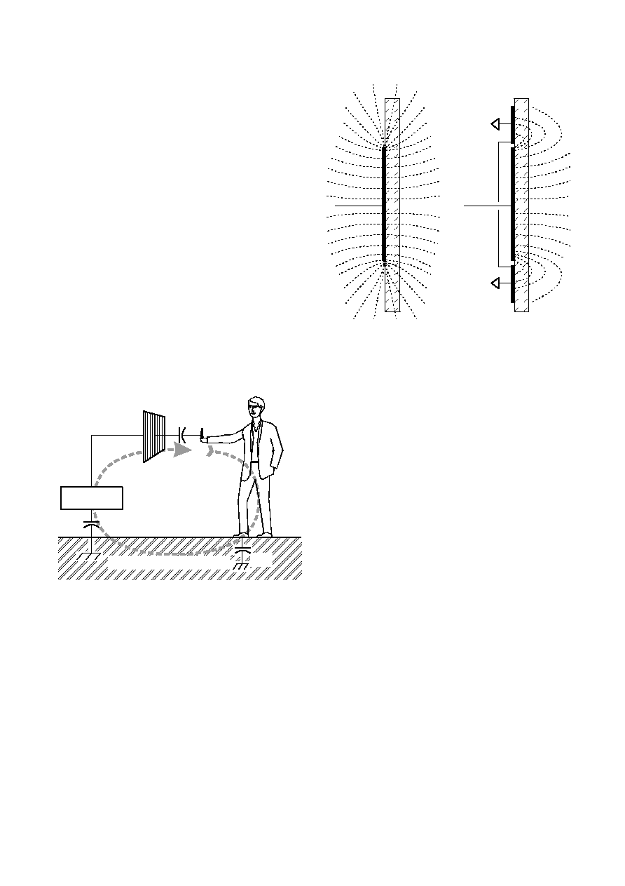
Like all capacitance sensors, these parts rely on Kirchoff's
Current Law (Figure 1-5) to detect the change in capacitance
of the electrode. This law as applied to capacitive sensing
requires that the sensor's field current must complete a loop,
returning back to its source in order for capacitance to be
sensed. Although most designers relate to Kirchoff's law with
regard to hardwired circuits, it applies equally to capacitive
field flows. By implication it requires that the signal ground
and the target object must both be coupled together in some
manner for a capacitive sensor to operate properly. Note that
there is no need to provide actual hardwired ground
connections; capacitive coupling to ground (Cx1) is always
sufficient, even if the coupling might seem very tenuous. For
example, powering the sensor via an isolated transformer
will provide ample ground coupling, since there is
capacitance between the windings and/or the transformer
core, and from the power wiring itself directly to 'local earth'.
Even when battery powered, just the physical size of the
PCB and the object into which the electronics is embedded
will generally be enough to couple a few
picofarads back to local earth.
Electrodes connected to the IC
themselves act as coupling plates back
to local ground, since when one
channel is sensing the other channels
are clamped to circuit ground.
1.3.4 V
IRTUAL
C
APACITIVE
G
ROUNDS
When detecting human contact (e.g. a
fingertip), grounding of the person is
never required. The human body
naturally has several hundred
picofarads of `free space' capacitance
to the local environment (Cx3 in Figure
1-5), which is more than two orders of
magnitude greater than that required to
create a return path to the IC via earth.
The PCB however can be physically
quite small, so there may be little `free
space' coupling (Cx1 in Figure 1-5)
between it and the environment to
complete the return path. If the circuit ground cannot be
earth grounded by wire, for example via the supply
connections, then a `virtual capacitive ground' may be
required to increase return coupling.
A `virtual capacitive ground' can be created by connecting
the IC's own circuit ground to:
(1) A nearby piece of metal or metallized housing;
(2) A floating conductive ground plane;
(3) A nail driven into a wall;
(4) A larger electronic device (to which its output might be
connected anyway).
Free-floating ground planes such as metal foils should
maximize exposed surface area in a flat plane if possible. A
square of metal foil will have little effect if it is rolled up or
crumpled into a ball. Virtual ground planes are more effective
and can be made smaller if they are physically bonded to
other surfaces, for example a wall or floor.
1.3.5 F
IELD
S
HAPING
The electrode can be prevented from sensing in undesired
directions with the assistance of metal shielding connected
l
Q
3
QT160/161 1.06/1102
Figure 1-2 Internal Switching & Timing
C
s
C
x
SNS2
SNS1
ELECTRODE
S
i
ngl
e
-
S
l
o
pe 14
-
b
i
t
S
w
i
t
ch
e
d
Ca
p
a
c
i
to
r
A
D
C
C harg e
Am p
B
u
rs
t
C
ont
rol
l
er
Result
Done
Start
Figure 1-3 Mesh Key Geometry
Figure 1-4 Open Electrode for Back-Illumination
to circuit ground (Figure 1-6). For example, on flat surfaces,
the field can spread laterally and create a larger touch area
than desired. To stop field spreading, it is only necessary to
surround the touch electrode on all sides with a ring of metal
connected to circuit ground; the ring can be on the same or
opposite side from the electrode. The ring will kill field
spreading from that point outwards.
If one side of the panel to which the electrode is fixed has
moving traffic near it, these objects can cause inadvertent
detections. This is called `walk-by' and is caused by the fact
that the fields radiate from either surface of the electrode
equally well. Again, shielding in the form of a metal sheet or
foil connected to circuit ground will prevent walk-by; putting a
small air gap between the grounded shield and the electrode
will keep the value of Cx lower and is encouraged. In the
case of the QT160/161, sensitivity can be high enough
(depending on Cx and Cs) that 'walk-by' signals are a
concern; if this is a problem, then some form of rear
shielding may be required.
1.3.6 S
ENSITIVITY
Sensitivity can be altered to suit various applications and
situations on a channel-by-channel basis. The easiest and
most direct way to impact sensitivity is to alter the value of
Cs. More Cs yields higher sensitivity.
1.3.6.1 Alternative Ways to Increase Sensitivity
Sensitivity can also be increased by using bigger electrodes,
reducing panel thickness, or altering panel composition.
Increasing electrode size can have diminishing returns, as
high values of Cx counteract sensor gain. Also, increasing
the electrode's surface area will not substantially increase
touch sensitivity if its diameter is already much larger in
surface area than the object being detected. The panel or
other intervening material can be made thinner, but again
there are diminishing rewards for doing so. Panel material
can also be changed to one having a higher dielectric
constant, which will help propagate the field through to the
front. Locally adding some conductive material to the panel
(conductive materials essentially have an infinite dielectric
constant) will also help; for example, adding carbon or metal
fibers to a plastic panel will greatly increase frontal field
strength, even if the fiber density is too low to make the
plastic bulk-conductive.
1.3.6.2 Decreasing Sensitivity
In some cases the QT160 may be too sensitive. In this case
gain can be lowered further by a number of strategies:
a) making the electrode smaller, b) making the electrode into
a sparse mesh using a high space-to-conductor ratio (Figure
1-3), or c) by decreasing the Cs capacitors.
2 - QT160/QT161 SPECIFICS
2.1 SIGNAL PROCESSING
The QT160 processes all signals using 16 bit math, using a
number of algorithms pioneered by Quantum. The algorithms
are specifically designed to provide for high survivability in
the face of adverse environmental changes.
2.1.1 D
RIFT
C
OMPENSATION
A
LGORITHM
Signal drift can occur because of changes in Cx, Cs, and
Vdd over time. If a low grade Cs capacitor is chosen, the
signal can drift greatly with temperature. If keys are subject
to extremes of temperature and humidity, the signal can also
shift. It is crucial that drift be compensated, else false
detections, non-detections, and sensitivity shifts will follow.
Drift compensation (Figure 2-1) is a method that makes the
reference level track the raw signal at a slow rate, only while
no detection is in effect. The rate of reference adjustment
must be performed slowly else legitimate detections can also
be ignored. The IC drift compensates each channel
independently using a slew-rate limited change to the
reference level; the threshold and hysteresis values are
slaved to this reference.
Once an object is sensed, the drift compensation
mechanism ceases since the signal is legitimately high, and
therefore should not cause the reference level to change.
The signal drift compensation is 'asymmetric'; the reference
level drift-compensates in one direction faster than it does in
the other. Specifically, it compensates faster for decreasing
signals than for increasing signals. Increasing signals should
not be compensated for quickly, since an approaching finger
l
Q
4
QT160/161 1.06/1102
Figure 1-6 Shielding Against Fringe Fields
Sense
wire
Sense
wire
Figure 1-5 Kirchoff's Current Law
Sense E lectrode
C
X2
Su rro un d ing e n v iro n m e n t
C
X3
SENSOR
C
X1

could be compensated for partially or entirely before even
approaching the sense electrode. However, an obstruction
over the sense pad, for which the sensor has already made
full allowance for, could suddenly be removed leaving the
sensor with an artificially elevated reference level and thus
become insensitive to touch. In this latter case, the sensor
will compensate for the object's removal very quickly, usually
in only a few seconds.
With large values of Cs and small values of Cx, drift
compensation will appear to operate more slowly than with
the converse.
2.1.2 T
HRESHOLD
C
ALCULATION
The internal threshold level is fixed at 6 counts for all
channels. These IC's employ a fixed hysteresis of 2 counts
below the threshold (33%).
2.1.3 M
AX
O
N
-D
URATION
If an object or material contacts a sense pad the signal may
rise enough to trigger an output, preventing further normal
operation. To prevent this `stuck key' condition, the sensor
includes a timer on each channel to monitors detections. If a
detection exceeds the timer setting, the timer causes the
sensor to perform a full recalibration (when not set to
infinite). This is known as the Max On-Duration feature.
After the Max On-Duration interval, the sensor channel will
once again function normally, even if partially or fully
obstructed, to the best of its ability given electrode
conditions. There are three timeout durations available via
strap option: 10s, 60s, and infinite (disabled) (Table 2-1).
Max On-Duration works independently per channel; a
timeout on one channel has no effect on another channel
except when the AKS feature is impacted on an adjacent
key. Note also that the timings in Table 2-1 are dependent
on the oscillator frequency: Doubling the recommended
frequency will halve the timeouts.
Infinite timeout is useful in applications where a prolonged
detection can occur and where the output must reflect the
detection no matter how long. In infinite timeout mode, the
designer should take care to be sure that drift in Cs, Cx, and
Vdd do not cause the device to `stick on' inadvertently even
when the target object is removed from the sense field.
The delay timings for max on-duration will increase if the
total duration of all bursts is greater than 33ms, i.e. an
average of 5.5ms per channel.
2.1.4 D
ETECTION
I
NTEGRATOR
It is desirable to suppress detections generated by electrical
noise or from quick brushes with an object. To accomplish
this, the IC's incorporate a detect integration
counter that increments with each detection until a
limit is reached, after which the output is activated.
If no detection is sensed prior to the final count, the
counter is reset immediately to zero. In the
QT160/161, the required count is 3.
The Detection Integrator can also be viewed as a
'consensus' filter, that requires three detections in
three successive bursts to create an output.
2.1.5 F
ORCED
S
ENSOR
R
ECALIBRATION
Pin 28 is a Reset pin, active-low, which in cases
where power is clean can be simply tied to Vdd. On
power-up, the device will automatically recalibrate
all 6 channels of sensing.
Pin 28 can also be controlled by logic or a microcontroller to
force the chip to recalibrate, by toggling it low for 5µs then
raising it high again.
The option pins are read by the IC once each acquisition
cycle and can be changed during operation.
2.1.6 R
ESPONSE
T
IME
Response time is fixed at 99ms at a 10MHz clock. Response
time can be altered by changing the clock frequency.
Doubling the recommended clock frequency to 20MHz will
halve the response time to 49ms.
Response time will become slower if the total duration of all
bursts is greater than 33ms, i.e. an average of 5.5ms per
channel.
2.2 OUTPUT FEATURES
The ICs are designed for maximum flexibility and can
accommodate most popular sensing requirements. These
are selectable using strap options on pins OPT1 and OPT2.
All options are shown in Table 2-1.
2.2.1 DC M
ODE
O
UTPUT
The outputs of these ICs can respond in a DC mode, where
they are active upon detection. The output will remain active
for the duration of the detection, or until the Max On-Duration
expires (if not infinite), whichever occurs first. If a max
on-duration timeout occurs first, the sensor performs a full
recalibration and the output becomes inactive until the next
detection.
2.2.2 T
OGGLE
M
ODE
O
UTPUT
This makes the sensor respond in an on/off mode like a flip
flop. It is most useful for controlling power loads, for example
in kitchen appliances, power tools, light switches, etc.
Max On-Duration in Toggle mode is fixed at 10 seconds.
When a timeout occurs, the sensor recalibrates but leaves
the output state unchanged.
2.2.3 O
UTPUT
D
RIVE
The outputs are active-high and can source 1mA and sink
5mA of non-inductive current. If inductive loads are used,
such as small relays, the inductances should be diode
clamped to prevent damage. When set to operate in a
proximity mode (at high gain) Out currents should be limited
to 1mA to prevent gain shifting side effects from occurring,
which happens when the load current creates voltage drops
on the die and bonding wires; these small shifts can
materially influence the signal level to cause detection
instability as described below.
l
Q
5
QT160/161 1.06/1102
Figure 2-1 Drift Compensation
Threshold
Signal
H ysteresis
R eference
Output

Care should be taken when the IC and the loads are both
powered from the same supply, and the supply is minimally
regulated. The QT160/161 derives its internal references
from the power supply, and sensitivity shifts can occur with
changes in Vdd, as happens when loads are switched on.
This can induce detection `cycling', whereby an object is
detected, the load is turned on, the supply sags, the
detection is no longer sensed, the load is turned off, the
supply rises and the object is reacquired, ad infinitum. To
prevent this occurrence, the Out pins should only be lightly
loaded if the device is operated from an unregulated supply,
e.g. batteries. Detection `stiction', the opposite effect, can
occur if a load is shed when an Out pin is active.
The outputs of the IC can directly drive LEDs with series
resistors. The LEDs should be connected with anodes to the
outputs and cathodes towards Vss, so that it lights when the
sensor is active.
2.3 AKSTM - Adjacent Key suppression
The QT160 (not QT161) features adjacent key suppression
for use in applications where keys are tightly spaced. If keys
are very close and a large finger touches one key, the keys
on either side might also activate. AKS stops detections on
adjacent keys by comparing relative signal levels among
them and choosing the key with the largest signal strength.
Key number 1 will cause a suppression of keys 6 and 2. Key
number 2 will cause a suppression of keys 1 and 3. Key 3
will cause a suppression of keys 2 and 4 and so on.
When a touch is detected on a key, but just before the
corresponding OUT pin is activated, a check is made for a
detection on the adjacent keys. If OUT is active on one or
both of the adjacent keys, or if a signal of greater strength is
found on them, the key is suppressed. This means that it is
not possible to activate both keys 3 and 4 for example; if 4 is
already on when 3 is touched, key 3 will be suppressed.
Likewise, if keys 3 and 4 are both touched, but 3 has a
weaker signal than 4 at the moment the decision is made,
then only key 4 will detect and 3 will be suppressed. Once
the detected key is released, the other key is free to detect.
Drift compensation also ceases for the key or keys which
have been suppressed, so long the signal on it is greater
than its threshold level.
This feature is also very effective on water films which bridge
over adjacent keys. When touching one key a water film will
`transport' the touch to the adjacent keys covered by the
same film. These side keys will receive less signal strength
than the key actually being touched, and so they will be
suppressed even if the signal they are detecting is large
enough to otherwise cause an output.
3 - CIRCUIT GUIDELINES
3.1 SAMPLE CAPACITOR
Charge sampler caps Cs can be virtually any plastic film or
low to medium-K ceramic capacitor. The acceptable Cs
range is from 10nF to 47nF depending on the sensitivity
required; larger values of Cs demand higher stability to
ensure reliable sensing. Acceptable capacitor types include
polyester film, PPS film, or NP0 / C0G ceramic.
3.2 OPTION STRAPPING
The option pins OPT1 and OPT2 should never be left
floating. If they are floated, the device can draw excess
power and the options will not be properly read.
See Table 2-1 for options. Note that the timings shown are
depend inversely on the oscillator frequency: Doubling the
recommended frequency will halve the timeouts.
3.3 POWER SUPPLY, PCB LAYOUT
The power supply can range from 4.5 to 5.5 volts. If this
fluctuates slowly with temperature, the QT160/161 will track
and compensate for these changes automatically with only
minor changes in sensitivity.
If the power supply is shared with another electronic system,
care should be taken to assure that the supply is free of
digital spikes, sags, and surges which can adversely affect
the IC. The QT160/161 will track slow changes in Vdd, but it
can be seriously affected by rapid voltage steps.
The supply is best locally regulated using a conventional
78L05 type regulator, or almost any 3-terminal LDO device
from 3V to 5V.
For proper operation a 0.1µF or greater bypass capacitor
should be used between Vdd and Vss; the bypass cap
should be placed very close to the device's power pins.
3.4 OSCILLATOR
The oscillator should be a 10MHz resonator with ceramic
capacitors to ground on each side. 3-pin resonators with
built-in capacitors designed for the purpose are inexpensive
and commonly found. Manufacturers include AVX, Murata,
Panasonic, etc.
Alternatively an external clock source can be used in lieu of
a resonator. The OSC_I pin should be connected to the
external clock, and OSC_O should be left unconnected.
These ICs are fully synchronous, clocked devices that
operate all sections from the OSC_I clock. If the frequency of
OSC_I is changed, all timings will also change in direct
proportion, from the charge and transfer times to the
detection response times and the max on-duration timings.
3.5 UNUSED CHANNELS
Unused signal channels should not be left open. They
should have a small value non-critical dummy Cs capacitor
connected to their SNS pins to allow the internal circuit to
continue to function properly. A nominal value of 1nF
(1,000pF) X7R will suffice.
Unused channels should not have sense traces or
electrodes connected to them.
l
Q
6
QT160/161 1.06/1102
infinite
Gnd
Gnd
DC Out
10s
Vdd
Vdd
Toggle
60s
Gnd
Vdd
DC Out
10s
Vdd
Gnd
DC Out
Max On-Duration
OPT2
OPT1
Table 2-1 Strap Options

3.6 ESD PROTECTION
In cases where the electrode is placed behind a dielectric
panel, the IC will be protected from direct static discharge.
However even with a panel, transients can still flow into the
electrodes via induction, or in extreme cases via dielectric
breakdown. Porous materials may allow a spark to tunnel
right through the material. Testing is required to reveal any
problems. The device does have diode protection on its SNS
pins which absorb and protect the device from most induced
discharges, up to 20mA; the usefulness of the internal
clamping will depending on the dielectric properties, panel
thickness, and rise time of the ESD transients.
In extreme cases ESD dissipation can be aided further with
added series resistors in line with the electrodes as shown in
Figure 1-1. Because the charge time is 1.2 µs, the circuit can
tolerate large values of series-R, up to 20k ohms in cases
where electrode Cx load is below 10pF. Extra diode
protection at the electrodes can also be used, but this often
leads to additional RFI problems as the diodes will rectify RF
signals into DC which will disturb the measurement.
Directly placing semiconductor transient protection devices
or MOV's on the sense leads is not advised; these devices
have extremely large amounts of nonlinear parasitic C which
will swamp the capacitance of the electrode.
Series-R's should be low enough to permit at least 6 RC
time-constants to occur during the charge and transfer
phases, where R is the added series-R and C is the load Cx.
If the device is connected to an external control circuit via a
cable or long twisted pair, it is possible for ground-bounce to
cause damage to the Out pins and/or interfere with key
sensing. Noise current injection into the power supply is best
dealt with by shunting the noise aside to chassis ground with
capacitors, and limited using resistors or ferrites.
3.7 RFI PROTECTION
PCB layout, grounding, and the structure of the input circuitry
have a great bearing on the success of a design that can
withstand strong RF interference.
The circuit is remarkably immune to RFI provided that certain
design rules be adhered to:
1. Use SMT components to minimize lead lengths.
2. Always use a ground plane under and around the circuit
and along the sense lines, that is as unbroken as
possible except for relief under and beside the sense
lines to reduce total Cx. Relieved rear ground planes
should be `mended' by bridging over them at 1cm
intervals with 0.5mm `rungs' like a ladder.
3. Ground planes should be connected only to a common
point near the Vss pins of the IC.
4. Route sense traces away from other traces or wires that
are connected to other circuits.
5. Sense electrodes should be kept away from other
circuits and grounds which are not directly connected to
the sensor's own circuit ground; other grounds will
appear to float at high frequencies and couple RF
currents into the sense lines.
6. Keep the 6 Cs sampling capacitors and all series-R
components close to the IC.
7. Use a 0.1µF minimum ceramic bypass cap very close to
the QT160/161 supply pins.
8. Use series-R's in the sense lines, of as large a value as
the circuit can tolerate.
9. Bypass input power to chassis ground and again at
circuit ground to reduce line-injected noise effects.
Ferrites over the power wiring may be required to
attenuate line injected noise.
Achieving RF immunity mostly requires diligence and a good
working knowledge of grounding, shielding, and layout
techniques.
l
Q
7
QT160/161 1.06/1102

4.1 ABSOLUTE MAXIMUM SPECIFICATIONS
Operating temp. . . . . . . . . . . . . . . . . . . . . . . . . . . . . . . . . . . . . . . . . . . . . . . . . . . . . . . . . . . . . . . . . . as designated by suffix
Storage temp. . . . . . . . . . . . . . . . . . . . . . . . . . . . . . . . . . . . . . . . . . . . . . . . . . . . . . . . . . . . . . . . . . . . . . . . . -55
O
C to +125
O
C
V
DD
. . . . . . . . . . . . . . . . . . . . . . . . . . . . . . . . . . . . . . . . . . . . . . . . . . . . . . . . . . . . . . . . . . . . . . . . . . . . . . . . . . . . . -0.5 to +7.0V
Max continuous pin current, any control or drive pin. . . . . . . . . . . . . . . . . . . . . . . . . . . . . . . . . . . . . . . . . . . . . . . . . ±20mA
Short circuit duration to ground, any pin. . . . . . . . . . . . . . . . . . . . . . . . . . . . . . . . . . . . . . . . . . . . . . . . . . . . . . . . . . . . infinite
Short circuit duration to V
DD
, any pin. . . . . . . . . . . . . . . . . . . . . . . . . . . . . . . . . . . . . . . . . . . . . . . . . . . . . . . . . . . . . . infinite
Voltage forced onto any pin. . . . . . . . . . . . . . . . . . . . . . . . . . . . . . . . . . . . . . . . . . . . . . . . . . . . . -0.6V to (Vdd + 0.6) Volts
4.2 RECOMMENDED OPERATING CONDITIONS
V
DD
. . . . . . . . . . . . . . . . . . . . . . . . . . . . . . . . . . . . . . . . . . . . . . . . . . . . . . . . . . . . . . . . . . . . . . . . . . . . . . . . . . . . . . +3.0 to 5.5V
Operating temperature range, 4.5V - 5.5V (QT160-AS, QT161-AS). . . . . . . . . . . . . . . . . . . . . . . . . . . . . . . -40 - +105C
Operating temperature range, 3.0V - 4.5V (QT160-AS, QT161-AS). . . . . . . . . . . . . . . . . . . . . . . . . . . . . . . . -40 - +85C
Operating temperature range (QT160-D, QT161-D). . . . . . . . . . . . . . . . . . . . . . . . . . . . . . . . . . . . . . . . . . . . . . . 0 - +70C
Operating frequency, 4.5V - 5.5V. . . . . . . . . . . . . . . . . . . . . . . . . . . . . . . . . . . . . . . . . . . . . . . . . . . . . . . . . . . . . . 4 - 20MHz
Operating frequency, 3.0V - 5.5V. . . . . . . . . . . . . . . . . . . . . . . . . . . . . . . . . . . . . . . . . . . . . . . . . . . . . . . . . . . . . . 4 - 10MHz
Short-term supply ripple+noise. . . . . . . . . . . . . . . . . . . . . . . . . . . . . . . . . . . . . . . . . . . . . . . . . . . . . . . . . . . . . . . . . . ±5mV/s
Long-term supply stability. . . . . . . . . . . . . . . . . . . . . . . . . . . . . . . . . . . . . . . . . . . . . . . . . . . . . . . . . . . . . . . . . . . . . . ±100mV
Cs value. . . . . . . . . . . . . . . . . . . . . . . . . . . . . . . . . . . . . . . . . . . . . . . . . . . . . . . . . . . . . . . . . . . . . . . . . . . . . . . . 1nF to 200nF
Cx value. . . . . . . . . . . . . . . . . . . . . . . . . . . . . . . . . . . . . . . . . . . . . . . . . . . . . . . . . . . . . . . . . . . . . . . . . . . . . . . . . . . 0 to 100pF
4.3 AC SPECIFICATIONS
Vdd = 5.0, Ta = recommended
, Cx = 5pF, Cs = 39nF, Fosc = 10MHz
Including detection integrator
ms
99
Response time
T
R
Before all timings degrade
ms
5.5
0.1
Allowable burst duration range
T
BLMR
counts
1,000
Burst length, each channel
N
BL
ms
3
Burst duration, each channel
T
BL
ms
33
Burst spacing interval
T
BS
µs
1.6
Transfer duration
T
PT
µs
1.2
Charge duration
T
PC
ms
330
Recalibration time
T
RC
Notes
Units
Max
Typ
Min
Description
Parameter
4.4 DC SPECIFICATIONS
Vdd = 5.0V, Cs = 39nF, Cx = 5pF, Fosc = 10MHz, Ta = recommended range, unless otherwise noted
bits
14
10
Acquisition resolution
A
R
OPT1, OPT2
µA
±1
Input leakage current
I
IL
OUTn, 1mA source
V
Vdd-0.7
High output voltage
V
OH
OUTn, 4mA sink
V
0.6
Low output voltage
V
OL
OPT1, OPT2
V
2
High input logic level
V
HL
OPT1, OPT2
V
0.7
Low input logic level
V
IL
Req'd for startup, w/o reset circuit
V/s
100
Supply turn-on slope
V
DDS
mA
8
2.5
Supply current
I
DD
Notes
Units
Max
Typ
Min
Description
Parameter
l
Q
8
QT160/161 1.06/1102

4.5 SIGNAL PROCESSING
Option pin selected
secs
10, 60, infinite
Post-detection recalibration timer duration
ms/level
231
Negative drift compensation rate
ms/level
990
Positive drift compensation rate
samples
3
Consensus filter length (Detection integrator)
counts
2
Hysteresis
counts
6
Threshold differential
Notes
Units
Max
Typ
Min
Description
All curves at Vdd = 5.0V
Figure 4-1
Figure 4-2
Figure 4-3
l
Q
9
QT160/161 1.06/1102
Burst Duration vs. Cs, Cx
0
2000
4000
6000
8000
10000
12000
14000
16000
18000
0
10
20
30
40
50
Cx
B
u
r
s
t
D
u
r
a
t
i
on,
M
i
cr
osec
ond
s
Cs = 220nF
Cs = 100nF
Cs = 47nF
Cs = 39nF
Cs = 22nF
Cs = 10nF
Burst Duration vs. Cs, Cx
0
500
1000
1500
2000
2500
3000
3500
4000
0
10
20
30
40
50
Cx
Bur
s
t
D
u
r
a
t
i
o
n
,
M
i
cr
o
sec
ond
s
Cs = 47nF
Cs = 39nF
Cs = 22nF
Cs = 10nF
Burst Duration cs. Cs, Cx
0
2000
4000
6000
8000
10000
12000
14000
16000
18000
0
50
100
150
200
250
Cs, nF
Bur
s
t
Dur
a
t
i
on,
M
i
cr
os
eco
nd
s
Cx = 5pF
Cx = 10pF
Cx = 15pF
Cx = 22pF
Cx = 33pF
Cx = 47pF

5 - PACKAGE OUTLINES
Typical
0.013
0.008
Typical
0.203
0.203
Y
0.39
0.32
9.906
8.128
x
0.31
0.31
7.874
7.874
Aa
0.18
0.143
3.632
3.632
S1
0.145
0.125
3.683
3.175
S
-
0.015
-
0.381
r
0.14
0.125
3.556
3.175
R
BSC
0.1
0.1
BSC
2.54
2.54
F
Typical
0.065
0.04
Typical
1.651
1.016
L1
4 places
0.02
0.008
4 places
0.508
0.203
L
0.022
0.016
0.559
0.406
P
0.048
0.023
1.22
0.584
Q
BSC
1.3
1.3
BSC
33.02
33.02
m
1.395
1.385
35.179
34.163
M
0.33
0.31
8.382
7.874
A
0.295
0.28
7.493
7.112
a
Notes
Max
Min
Notes
Max
Min
Inches
Millimeters
SYMBOL
Package type: 28-Pin Dual-In-Line
L
D
2a
H
M
Base level
Seating level
h
e
E
W
¯
0.008
0.002
0.21
0.050
h
0.078
0.068
1.99
1.730
H
8∫
0∫
8∫
0∫
ÿ
0.009
0.005
0.22
0.130
e
0.037
0.022
0.95
0.550
E
0.015
0.010
0.38
0.250
L
0.026
0.026
0.65
0.650
D
0.212
0.205
5.38
5.200
2a
0.311
0.301
7.9
7.650
W
0.407
0.396
10.33
10.070
M
Notes
Max
Min
Notes
Max
Min
Inches
Millimeters
SYMBOL
Package type: 28-pin SSOP
l
Q
10
QT160/161 1.06/1102

7 - PIN LISTINGS
Reset / recalibrate (active low)
/RST
28
Oscillator input
OSC_I
27
Oscillator output
OSC_O
26
Option input 2
OPT2
25
Option input 1
OPT1
24
Detection output 6 (active high)
OUT6
23
Detection output 5 (active high)
OUT5
22
Detection output 4 (active high)
OUT4
21
Detection output 3 (active high)
OUT3
20
Detection output 2 (active high)
OUT2
19
Detection output 1 (active high)
OUT1
18
Channel 6 sense pin B
SNS6B
17
Channel 6 sense pin A to key
SNS6A
16
Channel 5 sense pin B
SNS5B
15
Negative power (Ground)
Vss
14
Channel 5 pin A to key
SNS5A
13
Channel 4 pin B
SNS4B
12
Channel 4 pin A to key
SNS4A
11
Channel 3 pin B
SNS3B
10
Channel 3 pin A to key
SNS3A
9
Channel 2 pin B
SNS2B
8
Channel 2 pin A to key
SNS2A
7
Channel 1 pin B
SNS1B
6
Channel 1 pin A to key
SNS1A
5
Positive power
Vdd
4
Positive power
Vdd
3
Negative power (Ground)
Vss
2
Negative power (Ground)
Vss
1
Function
Name
Pin
Table 7-2 Pin Descriptions - QT160-AS
Reset / recalibrate (active low)
/RST
28
Oscillator input
OSC_I
27
Oscillator output
OSC_O
26
Option input 2
OPT2
25
Option input 1
OPT1
24
Detection output 6 (active high)
OUT6
23
Detection output 5 (active high)
OUT5
22
Detection output 4 (active high)
OUT4
21
Detection output 3 (active high)
OUT3
20
Detection output 2 (active high)
OUT2
19
Detection output 1 (active high)
OUT1
18
Channel 6 pin B
SNS6B
17
Channel 6 pin A to key
SNS6A
16
Channel 5 pin B
SNS5B
15
Channel 5 pin A to key
SNS5A
14
Channel 4 pin B
SNS4B
13
Channel 4 pin A to key
SNS4A
12
Channel 3 pin B
SNS3B
11
Channel 3 pin A to key
SNS3A
10
Channel 2 pin B
SNS2B
9
Channel 2 pin A to key
SNS2A
8
Channel 1 pin B
SNS1B
7
Channel 1 pin A to key
SNS1A
6
Negative power (Ground)
Vss
5
Negative power (Ground)
Vss
4
Negative power (Ground)
Vss
3
Positive power
Vdd
2
Positive power
Vdd
1
Function
Name
Pin
Table 7-1 Pin Descriptions - QT160-D
8 - ORDERING INFORMATION
QT161-A
SSOP-28
-40 - 105C
QT161-AS
QT161
PDIP-28
0 - 70C
QT161-D
QT160-A
SSOP-28
-40 - 105C
QT160-AS
QT160
PDIP-28
0 - 70C
QT160-D
MARKING
PACKAGE
TEMP RANGE
PART
l
Q
11
QT160/161 1.06/1102

l
Q
Copyright © 2002 QRG Ltd. All rights reserved.
Patented and patents pending
Corporate Headquarters
1 Mitchell Point
Ensign Way, Hamble SO31 4RF
Great Britain
Tel: +44 (0)23 8056 5600 Fax: +44 (0)23 8045 3939
admin@qprox.com
www.qprox.com
North America
651 Holiday Drive Bldg. 5 / 300
Pittsburgh, PA 15220 USA
Tel: 412-391-7367 Fax: 412-291-1015
The specifications set out in this document are subject to change without notice. All products sold and services supplied by QRG are subject
to our Terms and Conditions of sale and supply of services which are available online at www.qprox.com and are supplied with every order
acknowledgment. QProx, QTouch, QMatrix, QLevel, and QSlide are trademarks of QRG. QRG products are not suitable for medical
(including life-saving equipment), safety or mission critical applications or other similar purposes. Except as expressly set out in QRG's
Terms and Conditions, no licenses to patents or other intellectual property of QRG (express or implied) are granted by QRG in connection
with the sale of QRG products or provision of QRG services. QRG will not be liable for customer product design and customers are entirely
responsible for their products and applications which incorporate QRG's products.