 | –≠–ª–µ–∫—Ç—Ä–æ–Ω–Ω—ã–π –∫–æ–º–ø–æ–Ω–µ–Ω—Ç: QT60320D | –°–∫–∞—á–∞—Ç—å:  PDF PDF  ZIP ZIP |

APPLICATIONS -
Automotive panels
Machine tools
ATM machines
Touch-screens
Appliance controls
Outdoor keypads
Security keypanels
Industrial keyboards
The QT60320D digital charge-transfer ("QT") QMatrixTM IC is designed to detect touch on up to 32 keys in a scanned X-Y matrix. It will
project the keys through almost any dielectric, like glass, plastic, stone, ceramic, and even most kinds of wood, up to thicknesses of
5 cm or more. The touch areas are defined as simple 2-part interdigitated electrodes of conductive material, like copper,
Indium-Tin-Oxide (ITO), or screened silver or carbon deposited on the rear of the control panel. Key sizes, shapes and placement are
almost entirely arbitrary; sizes and shapes of keys can be mixed within a single panel of keys and can vary by a factor of 20:1 or more
in area. The gain (sensitivity) and threshold of each key can be set individually via simple commands over the UART port, for example
via the freeware QmBtn program. Key setups are stored internally in an onboard eeprom and do not need to be reloaded.
The IC is designed specifically to work with appliances, ATM machines, security panels, portable instruments, machine tools, or
similar products that are subject to environmental 'challenges' or even physical attack. It permits the construction of 100% sealed,
watertight keypanels that are immune to environmental factors such as humidity and condensation, temperature, dirt accumulation, or
the physical deterioration of the panel surface from abrasion, chemicals, or abuse. To this end the QT60320D contains
Quantum-pioneered self-calibration, drift compensation, and digital filtering algorithms that make the sensing function extremely
robust and survivable.
The device can readily control keys over graphical LCD panels or LEDs when used with clear, conductive ITO electrodes. It does not
require 'chip on glass' or other exotic fabrication techniques, thus allowing the OEM to source the keymatrix from multiple vendors.
External circuitry consists of an opamp, a common PLD, and a quad fet switch, which can fit into a footprint of roughly 1 square inch
(6.5 sq. cm). The device also can control two status LEDs, and includes in addition 8 addressable output drive lines and 4 readable
spare input lines which can be used to control LEDs, LCDs, or other panel functions without requiring additional control lines from the
host CPU. It also makes available to the user 86 bytes of onboard writeable and readable eeprom via the serial interface, thus helping
to reduce system cost by eliminating extra components.
QT60320D technology makes use of an important new variant of charge-transfer sensing, transverse charge-transfer, in an XY format
that minimizes the number of required scan lines. Unlike older technologies it does not require one IC per key, and is cost competitive
even with some membrane technologies. In many cases it can also replace resistive XY sense elements commonly used in touch
screens, at a fraction of the price.
The QT60320D is an improved version of the QT60320C, having lower noise and wider temperature range than the original
part. Prior silicon versions will not be available after December 2003.
LQ
Copyright © 1999, 2001 Quantum Research Group Ltd
QT60320D R1.11/12.07.03
L
Q
QT60320D
32-K
EY
QM
ATRIX
TM C
HARGE
-T
RANSFER
IC
Creates 32 `touch buttons' through any dielectric
100% autocal for life - no adjustments required
'N' key rollover: senses all 32 keys in parallel
Keys individually adjustable for sensitivity
Mix 'n match key sizes & shapes in one panel
Tolerates a 20:1 variance in key sizes on a panel
Panel thicknesses to 5 cm or more
Back lit keys possible with ITO electrodes
LED status function drives
User-addressable multifunction drive pins
User-addressable internal eeprom
Simple, universal serial interface
5V single supply operation
44-pin TQFP package
One square inch (6.5 square cm) of PCB required
X5
X4
X3
X2
X1
Gnd
Vc
c
AI
N
I4
I3
I2
O2
O3
O4
L1
L2
Vcc
Gnd
Y1
Y2
Y3
Y4
X6
X7
X8
RST
Vcc
Gnd
XT2
XT1
RX
TX
O1
O5
O6
O7
O8
Vcc
AGnd
Aref
CS
CC2
CC1
I1
1
2
3
4
5
6
7
8
9
10
11
23
24
25
26
27
28
29
30
31
32
33
44 43 42 41 40 39 38 37 36
34
35
12 13 14
22
21
19 20
18
17
16
15
QT60320
QT60320D-AS
-40
0
C to +105
0
C
TQFP
T
A
AVAILABLE OPTIONS
1 - OVERVIEW
The QT60320D is a digital burst mode charge-transfer (QT)
sensor designed specifically for matrix geometry touch
controls; it includes all signal processing functions necessary
to provide stable sensing under a wide variety of changing
conditions. Only a few low cost external parts are required for
operation. The entire circuit can be built within about 1
square inch of PCB area (smt).
The 60320 uses burst-mode charge transfer methods
pioneered and patented by Quantum, including charge
cancellation methods which allow for a wide range of key
sizes and shapes to be mixed together in a single keypanel.
These features permit the construction of entirely new
classes of keypanels never before contemplated, such as
touch-sliders, back-illuminated keys, and arbitrary shape
keypanels, all at very low cost.
The QT60320D uses an asynchronous serial (uart) interface
running at 9600 baud to allow key data to be extracted and to
permit individual key parameter setup. The interface protocol
uses simple ASCII commands and responds with either
ASCII or binary results depending on the command.
In addition to normal operating and setup commands the
device can also report back actual key signal strength and
error codes. Spare eeprom memory (over 80 bytes) can also
be written to and read to save the system designer from
having to install and interface to a separate eeprom.
The IC also includes 4 readable input (I1..I4) pins and 8
settable output (O1..O4) pins which can be used in any way
desired, including to scan a secondary keypad of up to 32
contact closures. Alternatively they can be used to remotely
activate panel LEDs, buzzers, or other types of indicators.
QmBtn software for the PC can be used to program a board
containing the IC as well as read back key status and signal
levels in real time.
The QT60320D employs transverse charge-transfer ('QT')
sensing, a new technology that senses the charge forced
across an electrode set by a digital edge.
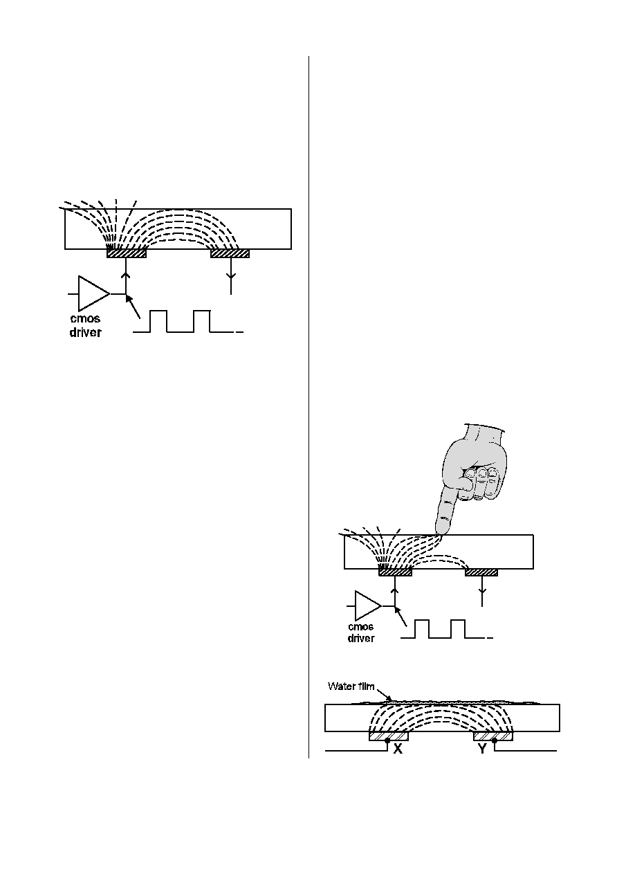
1.1 FIELD FLOWS
Figure 1-1 shows how charge is transferred across the
electrode set to permeate the overlying panel material; this
charge flow exhibits a rapid dQ/dt during the edge transitions
of the X drive pulse. The charge emitted by the X electrode is
partly received onto the corresponding Y electrode which is
then processed. The QT60320D matrix uses 8 'X'
edge-driven rows and 4 'Y' sense columns to allow up to 32
keys.
The charge flows are absorbed by the touch of a human
finger (Figure 1-2) resulting in a decrease in coupling from X
to Y; coupled charge increases in the presence of a
conductive film like water (Figure 1-3) which acts to bridge
the two elements. Increasing signals due to water films are
quite easy to discern and are not detected by the IC.
1.2 CIRCUIT MODEL
An electrical circuit model is shown in Figure 1-4. The
coupling capacitance between X and Y electrodes is
represented by Cx. While the reset switch is open, a
sampling switch is gated so that it transfers charge flows only
from the rising edge of X into the sample capacitor Cs. Cs is
a large value capacitor, typically in the range of 1 - 50nF. The
voltage rise captured on Cs after each X edge is quite small,
on the order of a millivolt, while changes due to touch are on
typically the order of 10's of microvolts. The X pulse can be
repeated in a burst consisting of up to several hundred
pulses to build up the voltage (and the change in voltage due
to touch) to a larger value. Longer bursts increase system
gain by collecting more charge; gain can thus be digitally
manipulated to achieve the required sensitivity on a
key-by-key basis during scanning.
If the voltage on Cs rises excessively it can fall outside of the
ADC's range. To reduce the voltage again without affecting
L
Q
2
QT60320D R1.11/12.07.03
Figure 1-2 Field Flows When Touched
Figure 1-3 Fields With a Conductive Film
overly ing panel
X
element
Y
element
Figure 1-1 Field flow between X and Y elements
overlying panel
X
element
Y
element
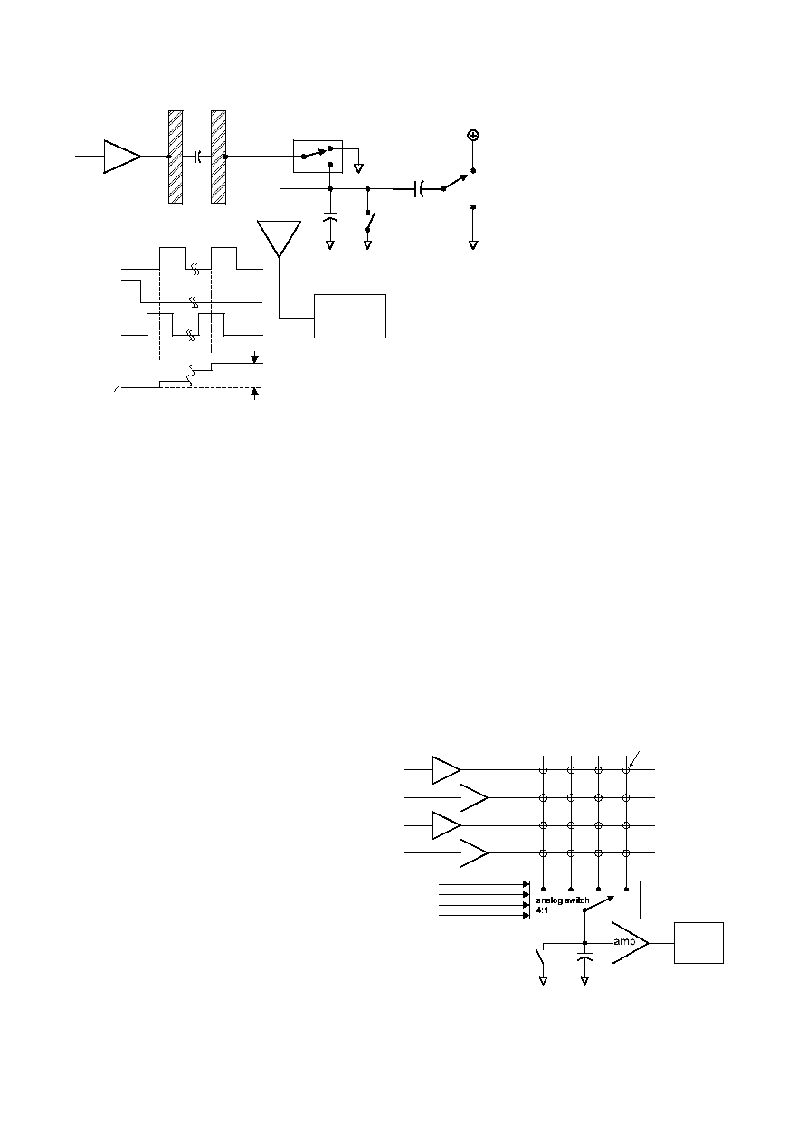
gain, one of two (or both) Cz capacitors can be switched to
subtract charge from Cs to create a negative-going offset,
bringing the signal back to a usable level. This action occurs
during the course of the burst and is not illustrated in the
timing diagram of Figure 1-4. This mechanism has the benefit
of allowing high levels of Cx while remaining highly sensitive
to small changes in charge coupling due to touch; the circuit
permits the designer to create very large, highly interdigitated
touch keys that are very sensitive.
The large Cs capacitor creates a virtual ground termination,
making the Y lines appear as a low impedance; this
effectively eliminates cross-coupling among Y lines due to
voltage spikes, while dramatically lowering susceptibility to
EMI. The circuit is also highly tolerant of capacitive loading
on the Y lines, since stray C from Y to ground appears
merely as a parallel capacitance to a much larger value of
Cs.
The QT60320D circuit design maintains high gain levels
independent of Cx or stray coupling C to ground. It also
readily compensates for field-related issues like
electrode design or the composition of the overlying
panel, as it has individual programmable gain and
threshold settings for each key.
Short sample gate dwell times after the X edge can be
used to limit the effect of moisture spreading from key
to key by taking advantage of the RC filter-like nature
of continuous films; the shorter the dwell time, the less
time that the charge has to travel through the
impedance of the film. This effect is completely
independent of the frequency of burst repetition,
intra-burst pulse spacing, or X drive pulse width.
Burst mode operation permits reduced power
consumption and reduces RF emissions, while
permitting excellent response time.
1.3 MATRIX CONFIGURATION
The matrix scanning configuration is shown in part in
Figure 1-5. The X drives are conventional CMOS
push-pull outputs which are sequentially
pulsed in groupings of bursts; a 4-pole
analog switch acts as the sample switch for
all 4 Y lines. At the intersection of each X
and Y line is an interdigitated electrode set
as shown in Figure 1-6. Typically the
outermost electrode is connected to X and
the inner electrode connected to Y.
Remaining Y lines not being sampled are
grounded.
1.4 'X' ELECTRODE DRIVES
The 8 'X' lines can be directly connected to
the matrix without buffering. Only the X lines'
positive edges are used to create the
transient field flows used to scan the keys.
Only one X line is active at a time, and it will
pulse for a burst length determined by the
'gain' setting parameter.
If desired an external 22V10 type CMOS
PLD can be used to create the short gate
dwell times necessary to enhance moisture
suppression (Section 1.2). The PLD takes
as its input all 'X' and 'Y' lines, and with
added RC time constants creates the
required short dwell time on the Y switches. The code for the
PLD is available freely on the Quantum web site and can also
be found in Section 5.
1.5 'Y' GATE DRIVES
There are 4 'Y' gate drives (Y1..Y4) which are active-high;
only one Y line is used during a burst for a particular key. The
chosen Y line goes high just before an X line transitions high,
and goes low again just after the X line rises. It is used to
gate on an analog switch, such as a 74HC4066, to capture
charge coupled through a key to the sample capacitor Cs.
An inverted version of the Y lines can be used to gate
unselected Y lines to ground, to suppress residual cross-key
coupling that might be caused by cross-pickup from adjacent
X drive traces. See Section 2.2.
L
Q
3
QT60320D R1.11/12.07.03
Figure 1-4 QT60320D Circuit Model
out
V
Am p
0
0
1
1
0
X drive (1 of 8)
Y
receive line
(1 of 4 )
X
electrode
Y
electrode
Sam p le
switch (1 o f 4)
Cx
C s
Re set
switch
Cz
(1 o f 2)
Cancellation
switch (1 o f 2)
8-bit ADC
X D rive
R ese t
sw itch
Sam ple
sw itch
Am p
out
Figure 1-5 QT60320D Matrix Configuration
X
1
X
2
X
3
X
4
Y
A D C
Y
s1
Y
s2
Y
s3
Y
s4
1
Y
2
Y
3
Y
4
Cs
R eset
switch
Interdigitated
keys
X drives
(4 of 8 shown)

Y gate signals can be manipulated externally so that the gate
dwell time is very short to suppress the effects of surface
conductivity due to water films. See Section 2.3.
1.6 SIGNAL PROCESSING
The QT60320D calibrates and processes all signals using a
number of algorithms pioneered by Quantum. These
algorithms are specifically designed to provide for high
survivability in the face of adverse environmental challenges.
1.6.1 S
ELF
-C
ALIBRATION
The QT60320D is fully self-calibrating. On powerup the IC
scans the matrix key by key and sets appropriate calibration
points for each in accordance with setup information in its
internal eeprom, or on the fly from a host MPU. Since the
circuit can tolerate a very wide dynamic range, it is capable of
adapting to a wide mix of key sizes and shapes having wildly
varying Cx coupling capacitances. No special operator or
factory calibration or circuit tweak is required to bring keys
into operation, except for a gain and threshold batch setup
which can be performed in seconds from a file saved on a
PC. Once set, there should never be a need to readjust these
parameters.
1.6.2 D
RIFT
C
OMPENSATION
A
LGORITHM
Signal drift can occur because of changes in Cx and Cs over
time. It is crucial that drift be compensated for, otherwise
false detections, non-detections, and sensitivity shifts will
follow.
Drift compensation (Figure 1-7) is performed by making the
reference level track the raw signal at a slow rate, but only
while there is no detection in effect. The rate of adjustment
must be performed slowly, otherwise legitimate detections
could be ignored. The QT60320D drift compensates using a
slew-rate limited change to the reference level; the threshold
and hysteresis values are slaved to this reference.
When a finger is sensed, the signal falls since the human
body acts to absorb charge from the cross-coupling between
X and Y lines. An isolated, untouched foreign object (a coin,
or a water film) will cause the signal to rise
slightly due to the enhanced coupling thus
created. These effects are contrary to the way
most capacitive sensors operate.
Once a finger is sensed, the drift compensation
mechanism ceases since the signal is
legitimately low, and therefore should not cause
the reference level to change.
The QT60320's drift compensation is
'asymmetric': the drift-compensation occurs in
one direction faster than it does in the other.
Specifically, it compensates faster for increasing
signals than for decreasing signals. Decreasing
signals should not be compensated for quickly,
since an approaching finger could be compensated for
partially or entirely before even touching the sense pad.
However, an obstruction over the sense pad, for which the
sensor has already made full allowance for, could suddenly
be removed leaving the sensor with an artificially suppressed
reference level and thus become insensitive to touch. In this
latter case, the sensor will compensate for the object's
removal by raising the reference level quickly.
1.6.3 T
HRESHOLD
AND
H
YSTERESIS
C
ALCULATIONS
The threshold value is established as an offset to the
reference level. As Cx and Cs drift, the reference drift
compensates with the changes and the threshold level is
automatically recomputed in real time so that it is never in
error. Since key touches result in negative signal swings, the
threshold is set below the signal reference level.
The QT60320D employs a hysteresis of 25% of the delta
between the reference and threshold levels. The signal must
rise by 25% of the distance from threshold to reference
before the detection event drops out and the key registers as
untouched.
1.6.4 M
AX
O
N
-D
URATION
If a foreign object contacts a key the signal may change
enough to create a 'false' detection lasting for the duration of
the contact. To overcome this, the IC includes a timer which
monitors detection duration. If a detection exceeds the timer
setting, the timer causes the sensor to perform a full
recalibration. This is known as the Max On-Duration feature.
After the Max On-Duration interval has expired and the
recalibration has taken place, the affected key will once again
function normally even if still contacted by the foreign object,
to the best of its ability. The Max On-Duration is fixed at 10
seconds of continuous detection.
1.6.5 D
ETECTION
I
NTEGRATOR
To suppress false detections caused by spurious events like
electrical noise, the QT60320D incorporates a detection
integration counter that increments with each detection
sample until a limit is reached, at which point a detection is
confirmed. If no detection is sensed on any of the samples
prior to the final count, the counter is reset immediately to
zero, forcing the process to restart. The required count is 4.
L
Q
4
QT60320D R1.11/12.07.03
Figure 1-7 Drift Compensation
Threshold
Signal
Hysteresis
Reference
Output
Figure 1-6 Sample Electrode Geometries
PARALLEL LINES
SERPENTINE
SPIRAL
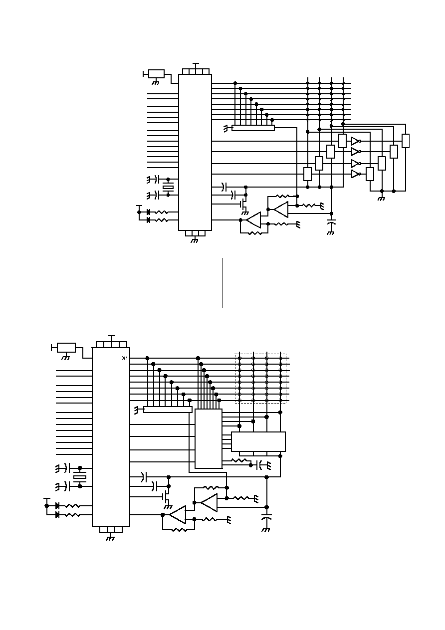
2 - CIRCUIT
SPECIFICS
A basic QT60320D circuit is
shown in Figure 2-1.
2.1 SIGNAL PATH
The QT60320D requires an
external sampling capacitor,
two Cz capacitors, an amplifier,
some analog switches, and an
R2R ladder DAC to operate.
The Cs capacitor performs the
charge integration function by
collecting charge coupled
though a selected key during
the dV/dt of the rising edge of
an 'X' scan line. The charge is
sampled 'n' times during the
course of a burst of switching
cycles of length 'n'. As the
burst progresses the charge on
Cs increases in a staircase
fashion (Figure 1-4).
At the burst's end the voltage
on Cs, which is on the order of
a few tenths of a volt, is
amplified by a gain circuit which includes an offset current
from the R2R ladder DAC driven by the X drive lines. The
offset current from the R2R ladder repositions the output of
the amplifier chain to coincide as closely as possible with the
center span of the 60320's ADC, which can convert voltages
between 0 and 5 volts. Between bursts the Cs reset mosfet is
activated to reset the Cs capacitor to ground.
Gain is directly controlled by burst length 'n', amplifier gain
Av, and the values of Cs, Cz1 and Cz2. Only 'n' can be
adjusted on a key by key basis whereas Av and the
capacitances can only be adjusted
for all keys. The amplifier should
typically have a total positive gain
of 100 +/- 20%..
If there is a large amount of
coupling between X and Y lines,
and where burst length 'n' is set to
a high number, charge
accumulation on Cs may reach a
point where the ladder DAC can no
longer offset the signal back into
the ADC's usable range. In this
case the circuit will employ one or
two of the Cz capacitors to 'knock
back' or cancel the charge
accumulated on Cs; each Cz will
cancel charge in a discrete step as
required.
L
Q
5
QT60320D R1.11/12.07.03
Figure 2-1 Basic QT60320D Circuit
X1
X2
X3
X4
X5
X6
X7
X8
YS1
YS2
YS3
YS4
CC 1
CC 2
C S
AIN
G G G G
V
V
V
Vcc
Vc
c
Rst
Rx
Tx
I1
I2
I3
I4
O 1
O 2
O 3
O 4
O 5
O 6
O 7
O 8
XT1
XT2
L1
L2
4
9
10
33
34
35
36
11
12
13
14
23
24
25
26
8
7
15
16
6 18
39
V
5 1 7 2 7
38
4 0
4 1
4 2
4 3
4 4
1
2
3
1 9
2 0
21
2 2
3 2
3 1
3 0
3 7
28
29
D S18 11
8MHz
CAL L ED
STAT LED
C6 (Cz1) 8 20pF
C7 (Cz2) 8 20pF
BSN20
R 2R d ac 1 00K
+
_
+
_
R3 68K
R 5 10K
R4 100K
R6 10K
C5 (Cs)
1 5nF
Vcc
1/
4
H
C
4066
1/4
H
C
40
66
1/4
H
C
40
66
1/4
H
C
406
6
TL C22 72
Q
T
60
32
0
U
S
E
R
PO
R
T
PI
N
S
UART I N
U ART OUT
V
Keymatrix
Y3
Y2
Y4
Y1
1/4
H
C
406
6
1/4
H
C
40
66
1/4
H
C
40
66
1/
4
H
C
4066
74 AC 04
Figure 2-2 Improved Circuit to Suppress Water Films
X2
X3
X4
X5
X6
X7
X8
YS1
Y S2
Y S3
Y S4
CC 1
CC 2
CS
AIN
G G G G
V
V
V
Vcc
Vc
c
R st
R x
Tx
I 1
I 2
I 3
I 4
O 1
O 2
O 3
O 4
O 5
O 6
O 7
O 8
XT1
XT2
L 1
L 2
4
9
1 0
3 3
3 4
3 5
3 6
11
1 2
1 3
1 4
2 3
2 4
2 5
2 6
8
7
1 5
1 6
6 18
39
V
5 17 27
3 8
40
41
42
43
44
1
2
3
19
20
21
22
32
31
30
37
28
2 9
D S18 11
8M H z
CAL L ED
STAT LED
C6 (Cz 1) 820pF
C 7 (Cz 2) 820p F
BSN 20
R 2R dac 100K
R 3 68 K
R 5 1 0K
R 4 100 K
R 6 10 K
C 5 (C s)
15nF
Vcc
TLC 2272
Q
T
60320
US
E
R
PO
R
T
P
I
N
S
UAR T IN
U ART OU T
V
Keymatrix
Y 3
Y 2
Y4
Y1
QS3125
I /O
I/O
I /O
I/O
I /O
I/O
I /O
I/O
E
E
E
E
22V10
R t
C t
+
_
+
_
Components shown in Figure 2-1 include:
An LVD reset (e.g. Dallas DS1811) suitable for 5 volt
supplies and an active-low on low-voltage output;
An R2R ladder network (CTS 750-107R100K or
equivalent);
A >2MHz GBW CMOS rail-rail output opamp capable of
sensing ground on the inputs;
An 8MHz crystal or resonator, or a ceramic resonator
with built-in capacitors;
Two indicator LEDs (optional) to show sensing state
and calibration status;
74AC04 inverters to drive the two banks of analog
switches in opposite states;
Two 74HC4066 analog switches;
A reset mosfet, most any small-signal mosfet with a
guaranteed on-state at 4 volts Vgs. The mosfet should
have an input capacitance (Ciss) of under 50pF for low
charge injection.
Components not shown are:
A +5 volt regulator (78L05 types are suitable);
Supply bypass capacitors (two 0.1uF X7R caps placed
near the 60320 and the 74HC4066's);
An RS232 level translator, like a MAX232 or
comparable device to allow communications over a
cable to a distant host device (if desired).
74HC4066 switches work fine but are less than ideal; these
switches have high levels of charge injection that will add to
the signal and also induce thermal drift. However these parts
provide a break-before-make action that is critical to
successful operation.
See Section 4 for more circuit specifics.
2.2 WATER SUPPRESSING CIRCUIT
A circuit that suppresses cross-coupling from key to key by
water films is shown in Figure 2-2. This circuit includes a
22V10 type CMOS PLD configured with an RC timing circuit
to shorten the dwell time of the Y gate pulses. This has the
effect of curtailing the charge collected from parts of a water
film that are distant from the key, thus reducing the
occurrence of cross-coupling among keys when the panel is
wet. Rt and Ct are adjusted to provide a timing delay of from
75ns to 100ns. This circuit is employed in Quantum's E6S3
eval board (Section 5).
The 22V10 creates a short delay from the rising edge of the
X line in use; this delayed signal is gated with the Y lines to
create new, foreshortened Y-gate signals (Figure 2-3).
A QualitySemi QS3125 'bus gate' (also: TI SN74CBT3125,
Pericom PI5C3125 or comparable) is used as a high
performance n-channel analog switch having near-zero
charge injection. The switch is only used as a charge drain to
near-ground potential, and so full bilateral 0-5V switch
operation is not required.
Source code for the 22V10 can be found in Section 5.
Representative parts include the Xilinx XCR22V10 and ICT's
PEEL22CV10AC-25. This device must have conventional
CMOS I/O structures to work properly.
Mechanical measures can also be used to suppress key
cross-coupling, for example raised plastic barriers between
keys (or placing keys in shallow wells) to lengthen the
electrical path from key to key, or simply increasing the key
spacing (and reducing key size).
See Section 4 for more circuit specifics.
2.3 CALIBRATION
The 60320 calibrates on power-up using algorithms that seek
out the optimal level of R2R offset and Cz cancellation on a
key-by-key basis. The algorithm uses a successive
approximation method, to calibrate all 32 keys in about one
second. The calibration data is not permanently stored; the
device recalibrates each time the unit powers up.
If a false calibration occurs due to a key touch or foreign
object on the keys during powerup, the affected key will
recalibrate again immediately when the object is removed. A
calibration cycle can also be induced via a serial command
from a host device.
2.4 X-Y TIMING
The basic timing diagram shown in Figure 2-3 relates to a
particular key being addressed by an X
A
drive line and a gate
control line Y
B
. The acquisition of a key is done using a
discrete burst of X pulses of length 'n', where 'n' is
programmable via the UART interface (and stored internally
in eeprom). The corresponding Y line for the sampled key is
also pulsed in quadrature so as to gate the external analog
switch, straddling the rising edge of Xa. At the end of the
burst, the X pins are used to drive the external R2R ladder
network which generates an offset to the amplifier chain. It is
during this period that the amplifier stabilizes and the signal
is sampled internally by the QT60320D.
Figure 2-3 also shows a dwell-adjusted version of Yb, Yb',
that can be generated with the help of external timing delays.
Yb' has a shortened dwell time with respect to Xa; this
shorter dwell time acts to suppress the effects of moisture on
the keyboard surface by foreshortening the charge transfer
process, which acts to limit the recovery of charge forced into
the water film by the rising edge of Xa.
L
Q
6
QT60320D R1.11/12.07.03
Figure 2-3 Timing of X and Y signals
Yb
Xa
Am p out
'n' pulses / burst
R2R Value
Xa
Yb
Yb'
Yb

Yb is used to gate another analog switch to ground, and if
the switches used do not have a break-before-make
characteristic, they should be guard-banded as shown to
prevent cross conduction from Cs to ground.
3 SERIAL INTERFACE
The QT60320D uses a serial interface to a host. This port
uses a simple ASCII protocol described in this section.
3.1 SERIAL PORT SPECIFICATIONS
The QT60320D uses a full-duplex asynchronous serial
interface with the following specifications:
Baud Rate:
9600
Parity:
None
Length:
8 bits
Stop bits:
1
These specifications hold if the device is operated from an
8MHz crystal or resonator.
The port can be directly connected to a like port of a host
MCU, or transmitted over a length of cable on a standard
RS232C interface to a PC or other device, with the aid of a
MAX232 type driver/receiver circuit.
3.2 COMMAND SET
The 60320 requires ASCII commands over the serial port in
order to send result data. The commands must be one of
those listed in Table 3-1. None of the commands should ever
be terminated with a CR or LF code. Each command is
self-contained and requires no terminator.
3.2.1 's' C
OMMAND
- B
UTTON
S
TATE
(Hex code 0x73) After an `s' character is received, the E6S3
reports back the touch-state of the buttons; it responds by
transmitting back 4 bytes of data containing a total of 32 data
bits, where each bit represents the state of one button (Table
3-2).
Each byte holds the state of the buttons contained in a Y
column. The first byte corresponds to column Y1 while the
4th byte corresponds to column Y4. Bit 0 of each byte holds
the state of the button corresponding to X1; bit 7 holds the
state corresponding to X8.
Multiple key presses will show as
multiple bits being set in the data stream. The device
supports n-key rollover to a limit of all 32 keys.
Example: The key at intersection X5/Y2 appears at bit 4 in
the second byte; if key X5/Y2 is touched the bit is set. All
untouched bits register as a `0'.
3.2.2 'S' C
OMMAND
- I
DENTIFICATION
R
EPORTING
(Hex code 0x53) The E6S3 board responds with the 7-byte
ASCII signature "32000xx" where x is the code revision.
3.2.3 'e' C
OMMAND
- E
RROR
R
EPORTING
(Hex code 0x65) This command allows the host to retrieve
the error status bits for all buttons, in 4 consecutive bytes
(Table 3-3). The byte and bit sequences are identical to that
described in conjunction with the 's' command (see prior).
The appropriate bits are set high when errors are detected.
The error may be caused either by a short across the button
or an open circuit at the button.
3.2.4 '/dXY' C
OMMAND
- D
ATA
S
IGNAL
R
EPORTING
(Hex codes 0x2F 0x64 X Y) This sequence reports back the
signal level and reference value for the key chosen. X and Y
are zero-referenced binary (not ASCII) values in the range
0..7 for X and 0..3 for Y to indicate the button for which data
is requested. If X=0 and Y=0, the device reports back with
the data for key X1 Y1. If X=3 and Y=1, the key selected is
X4 Y2. The last key is X8 Y4, so the highest /dXY command
is /d73 where '7' and '3' are in binary.
The device reports back with two bytes: the first is the
reference level, the second is the signal level. Both are
binary bytes of range 0..255.
3.2.5 '/DXY' C
OMMAND
- O
FFSET
&
C
OARSE
R
EPORTING
(Hex codes 0x2F 0x44 X Y) This
sequence reports back the fine offset
(R2R DAC) and coarse (Cz1, Cz2
bucking caps) values for the key
chosen. X and Y are zero- referenced
binary (not ASCII) values in the range
0..7 for X and 0..3 for Y to indicate the
button for which data is requested.
L
Q
7
QT60320D R1.11/12.07.03
Table 3-1 ASCII Command Set
Port Read.
Reads back the 4 bits of user port
pins I1..I4
0x49
I
Port Write.
Writes byte value v to the user
output pins O1..O8
0x4F v
Ov
Settings Write.
Writes the Gain or Threshold
value v for the chosen key at A
0x2F 0x45 A v
/EAv
Settings Reporting.
Returns Gain and Threshold
levels for chosen key at A
0x2F 0x65 A
/eA
Offset,Coarse Cal Reporting.
Returns coarse and offset values
for the key at location X Y
0x2F 0x44 X Y
/DXY
Data Signal Reporting.
Returns signal and reference for
the key at location X Y
0x2F 0x64 X Y
/dXY
Error reporting.
Returns 4 bytes corresponding to
error bits for each key
0x65
e
Identification command.
QT60320D responds with
signature "32000xx" where xx is
the code revision
0x53
S
Button State.
Returns 4 bytes of on/off status
for all buttons
0x73
s
Purpose
Hex
Code
ASCII
Code
Table 3-2 's' Command button state responses
X1/Y4
X2/Y4
X3/Y4
X4/Y4
X5/Y4
X6/Y4
X7/Y4
X8/Y4
4
X1/Y3
X2/Y3
X3/Y3
X4/Y3
X5/Y3
X6/Y3
X7/Y3
X8/Y3
3
X1/Y2
X2/Y2
X3/Y2
X4/Y2
X5/Y2
X6/Y2
X7/Y2
X8/Y2
2
X1/Y1
X2/Y1
X3/Y1
X4/Y1
X5/Y1
X6/Y1
X7/Y1
X8/Y1
1
BYTE #
0
1
2
3
4
5
6
7
BIT #

The device reports back with two bytes:
the first is the R2R offset DAC amount
(0..255), the second is the coarse
setting as a bit pattern: coarse bit 0
corresponds to Cz1, coarse bit 1 to
Cz2, resulting in valid data values of 0,
1, 3.
This information is useful in observing
circuit behavior for diagnostic purposes
during development. Values of Coarse
= 3 and Offset > 128 indicate excessive
X-to-Y coupling that can arise due to normal production
variances or component drift. The maximum limit the circuit
can tolerate is Coarse = 3, Offset = 255 before the signal
saturates and a key becomes inoperable.
3.2.6 '/eA' C
OMMAND
- S
ETTINGS
R
EPORTING
(Hex codes 0x2F 0x65 A) Allows the gain and threshold
settings for a specific button to be read back to the host. 'A' is
a single binary byte specifying the address of the data to be
read. Separate commands must be issued to read the gain
and threshold for each button as these values are held at
separate addresses, with the data for the threshold being
held in the address immediately following that for the gain.
The gain and threshold settings for all buttons are held in an
internal byte array, starting at address 100 (decimal). The
first two sequential bytes in this array hold the settings data
for button X1/Y1, the next two bytes hold the data for button
X2/Y1 and so on. The gain is held in the first byte (at the
lower address) and the threshold in the second byte.
The button memory addresses are calculated as follows for a
given key:
Multiply (X-1) times 2 to get M
So, if the key is on X6, M = (6-1)*2 = 10 (decimal).
Multiply (Y-1) times 16 to get N
So, if the key is on Y3, N = (3-1)*16 = 32 (decimal).
Add M + N + 100 to get the first of the two memory
addresses for the key.
Example: A key located at X4, Y3 would have its base
address at:
(4-1)*2 + (3-1)*16 + 100 = 32 + 6 + 100 = 138 (decimal)
The first byte, at address 138 decimal is the gain, while
address 139 has the threshold for X4/Y3. The address must
be sent as a binary number (packed into 8 bits, i.e. 0x8a and
0x8b in this example), NOT as the ASCII string `1 3 8'.
The QT60320D reports back with a single binary byte
containing the data requested.
3.2.7 EEPROM R
EAD
A
CCESS
VIA
/eA
It is possible to use part of the QT60320's internal eeprom as
'user storage'. This feature allows the elimination of a
separate eeprom associated with a host MCU, reducing
system cost. The QT60320D has 86 bytes of spare eeprom
available to the user for any function whatsoever. The
eeprom can be read and written using the same /eA and
/EAv commands used to examine and write key settings.
The first byte of eeprom is located at address 170 (decimal)
and can be read via the command string /eA where 'A' is the
binary byte 170 (0xaa). The highest location is at 255 (0xff).
3.2.8 '/EAv' C
OMMAND
- S
ETTINGS
W
RITE
(Hex codes 0x2F 0x45 A v) Allows the gain and threshold
settings for a button to be written. 'A' is a single binary byte
specifying the address and 'v' is a single binary byte value of
the data to be written.
The addresses are calculated in an identical manner to those
for the /eA command above.
Note that a change in the gain value of even one key will
cause the E6S3 to recalibrate all keys.
3.2.9 EEPROM W
RITE
A
CCESS
VIA
/EA
V
See 3.2.7 for information on reading eeprom data.
The /EAv command can be used to write a byte to any of the
86 available internal eeprom locations. Like the /eA
command, byte 'A' is the address of the byte from 0xaa to
0xff. The byte 'v' should contain the 8-bit binary data to be
written to the address 'A'.
The first byte of eeprom is located at address 170 (decimal)
and can be written via the command string /EA where 'A' is
the binary byte 170 (0xaa). The highest location is at 255
(0xff).
3.2.10 'Ov' C
OMMAND
- U
SER
P
ORT
W
RITE
(Hex codes 0x4F v) Writes the value `v', an 8-bit binary byte,
to the QT60320's 8 output port pins O1...O8.
This feature can be used to drive LED's via external buffers,
a self-oscillating acoustic sounder, or other peripheral device.
It can even be used in conjunction with the `I' command
(below) to scan a set of external electromechanical keys (up
to 32 switches, e.g. in an 8x4 matrix) near the panel.
3.2.11 'I' C
OMMAND
- U
SER
P
ORT
R
EAD
(Hex code 0x49) Causes the QT60320D to return a binary
byte from the port pins I1...I4. The value is returned in the
lower nibble (bits 0,1,2,3) of the return byte. The high 4 bits
are held at zero.
4 - CIRCUIT GUIDELINES
4.1 POWER SUPPLY, PCB LAYOUT
The power supply should be 5.0 volts +/- 10%. This can be
provided by a common 78L05 3-terminal regulator. LDO type
regulators are usually fine but can suffer from poor transient
load response; this will cause erratic key behavior.
If the power supply is shared with another electronic system,
care should be taken to assure that the supply is free of
digital spikes, sags, and surges which can adversely affect
the circuit. The QT60320D will track slow changes in Vcc, but
it can be adversely affected by rapid voltage steps and
impulse noise on the supply rail.
L
Q
8
QT60320D R1.11/12.07.03
Table 3-3 'e' Command error code responses
X1/Y4
X2/Y4
X3/Y4
X4/Y4
X5/Y4
X6/Y4
X7/Y4
X8/Y4
4
X1/Y3
X2/Y3
X3/Y3
X4/Y3
X5/Y3
X6/Y3
X7/Y3
X8/Y3
3
X1/Y2
X2/Y2
X3/Y2
X4/Y2
X5/Y2
X6/Y2
X7/Y2
X8/Y2
2
X1/Y1
X2/Y1
X3/Y1
X4/Y1
X5/Y1
X6/Y1
X7/Y1
X8/Y1
1
BYTE #
0
1
2
3
4
5
6
7
BIT #

4.2 SAMPLE CAPACITOR
Charge sampler Cs should be a PPS film or NPO ceramic
type for best stability. Acceptable Cs values range from 1nF
to 50nF. Lower values will increase circuit gain and hence
key sensitivity; lower values also act to reduce the required
burst length for a given desired sensitivity at the expense of
reduced inherent signal averaging.
4.3 C
Z
CAPACITORS
The two Cz capacitors should have a value of 4% to 6% of
the total value of Cs + Cz1 + Cz2. The objective is to allow
the creation of a negative voltage step at Cs of about 0.25
volts with each Cz cap switched.
In cases where the matrix is composed entirely of small keys,
the Cz caps may not actually fire, or perhaps only one of
them may fire. However, the device's error detection logic
requires the presence of these two capacitors in order to
function correctly.
If Cs = 15nF (a common value for the circuit), then each Cz
should be 820pF. The Cz capacitors should be of type NPO
or C0G ceramic, or PPS film.
4.4 R2R RESISTOR LADDER
The R2R resistor ladder network should be of value R=100K
ohms and have a precision of at least 7 bits. The nominal
resistance of the ladder is also the series impedance of the
ladder and affects the scaling of the offset injected into the
amplifier chain. The ladder should create an offset in the
output of the amplifier chain of about 0.15 volts / LSB. The
scaling of the offset injection also affects the crossover points
for the switching of each Cz capacitor. If during the
calibration cycle the R2R network is found to not provide
enough offset to bring the signal to the midpoint of the ADC's
range, a Cz capacitor will be switched in to create an
additional negative offset.
If the R2R value and Cz values are not properly matched, the
circuit may not be able to converge on a calibration point.
This will happen especially if the Cz cancellation voltage step
is too large.
4.5 AMPLIFIER
The amplifier chain should be as shown in the various figures
in this datasheet. It should have 2 stages of gain, totaling
about 100 +/-20%. Numerous opamps are available that will
perform to requirements, including the TI TLC2272 and the
Analog Devices OPA2340. The opamps should have at least
a rail-to-rail CMOS output, and an input that can sense from
ground to at least +1 volt. The recommended GBW is 2MHz
or above. To reduce leakage current problems the amplifier
should be a JFET or CMOS input type only.
4.6 ESD PROTECTION
In general the QT60320D will be protected from direct static
discharge by the overlying panel. However, even with a
panel, transients can still flow into the electrode via induction,
or in extreme cases, via dielectric breakdown. Porous
materials may allow a spark to tunnel right through the
material. Testing is required to reveal any problems. The
QT60320D does have diode protection on its terminals which
can absorb and protect the device from most induced
discharges, up to 20mA; the usefulness of the internal
clamping will depending on the dielectric properties, panel
thickness, rise time of the ESD transients, and their duration.
The device pins can be further protected by inserting series
resistance into the X lines; similarly, the charge capture
circuitry (the PLD and analog switch) can similarly benefit
from series-R in the Y lines. The resistances chosen should
not be so high as to interfere with the QT process. Every
board layout is different and thus it is difficult to specify a
suitable value, however, typical values range from 200 ohms
to 10K ohms. In serious cases additional low-capacitance
high-conductance clamp diodes (e.g. BAV99) may be added
to shunt ESD aside.
The QT60320's 'X' drive lines are always being driven at low
impedance; they are never 3-state unless the circuit is
powering up or is powered down. This is a considerable
advantage in dealing with ESD. The part's Y control pins do
not directly go to the matrix. The 4 user-input pins may be
vulnerable and should be resistor and/or diode protected if
they are in danger of being subject to ESD.
L
Q
9
QT60320D R1.11/12.07.03

5 EPLD SOURCE LISTING
Source listing for a ICT
PEEL22CV10AZ epld
. The EPLD functions to generate control signals for the QS3125 quad n-channel switch, to
clamp unused Y lines during scanning, and to control the Y gate dwell time after the rise of an X line. This latter feature allows for moisture
suppression since the charge transfer duration decreases (and thus is less responsive to the slow-moving charges from resistive water films)
with decreasing dwell time. Rt and Ct (R21 and C12 in the E6S3) govern this delay time after the rise of any X line.
_________________________________________________________
TITLE 'E6S3'
DESIGNER 'H Philipp & S Brunet'
DATE '12/03/01'
PEEL22CV10A
"I/O CONFIGURATION DECLARATION
"IOC (PIN_NO
'PIN_NAME'
POLARITY
OUTPUT_TYPE
FEEDBACK_TYPE )
"Inputs
XS1 PIN 8
"externally OR'd X inputs (8)
XS2 Pin 7
XS3 Pin 6
XS4 Pin 5
XS5 Pin 4
XS6 Pin 3
XS7 Pin 2
XS8 Pin 1
YS2 PIN 9
YS3 Pin 10
YS4 PIN 11
YS1 Pin 13
"Outputs
"Clamping outputs
IOC ( 22 'Y1'
Pos
Com
Feed_Pin )
IOC ( 20 'Y2'
Pos
Com
Feed_Pin )
IOC ( 19 'Y3'
Pos
Com
Feed_Pin )
IOC ( 17 'Y4'
Pos
Com
Feed_Pin )
"QS3125 drives
IOC ( 23 'F1'
Pos
OutCom Feed_Pin )
IOC ( 21 'F2'
Pos
OutCom Feed_Pin )
IOC ( 18 'F3'
Pos
OutCom Feed_Pin )
IOC ( 16 'F4'
Pos
OutCom Feed_Pin )
"Dly ckt in (& reset of delay cap drive out)
IOC ( 14 'XSD'
Pos
Com
Feed_Pin )
"Dly ckt drive out
IOC ( 15 'XSS'
Pos
OutCom Feed_Pin )
AR NODE 25 "Global Asynchronous Reset
SP NODE 26 "Global Synchronous Preset
EQUATIONS
AR = 0;
SP = 0;
y4.com = 0;
" Clamp outputs
y3.com = 0;
y2.com = 0;
y1.com = 0;
y4.oe = !ys4;
" drive outs to gnd when not used.
y3.oe = !ys3;
y2.oe = !ys2;
y1.oe = !ys1;
xss.com = xs1 # xs2 # xs3 # xs4 # xs5 # xs6 # xs7 # xs8; "sum all of x to drive out delay ckt
xsd.com = 0;
xsd.oe = !(xs1 # xs2 # xs3 # xs4 # xs5 # xs6 # xs7 # xs8); "clamp the delay cap when all 'xs' lines are 0
F4.com = !(ys4 & !xsd);
" enables to 3125 are active low
F3.com = !(ys3 & !xsd);
F2.com = !(ys2 & !xsd);
F1.com = !(ys1 & !xsd);
L
Q
10
QT60320D R1.11/12.07.03

6 E6S3 BOARD SCHEMATIC
L
Q
11
QT60320D R1.11/12.07.03

7.1 ABSOLUTE MAXIMUM SPECIFICATIONS
Operating temp. . . . . . . . . . . . . . . . . . . . . . . . . . . . . . . . . . . . . . . . . . . . . . . . . . . . . . . . . . . . . . . . . . . . . . . -40
O
C to +105
O
C
Storage temp. . . . . . . . . . . . . . . . . . . . . . . . . . . . . . . . . . . . . . . . . . . . . . . . . . . . . . . . . . . . . . . . . . . . . . . . . -55
O
C to +125
O
C
V
DD
. . . . . . . . . . . . . . . . . . . . . . . . . . . . . . . . . . . . . . . . . . . . . . . . . . . . . . . . . . . . . . . . . . . . . . . . . . . . . . . . . . . . -0.5 to +6.0V
Max continuous pin current, any control or drive pin. . . . . . . . . . . . . . . . . . . . . . . . . . . . . . . . . . . . . . . . . . . . . . . . ±20mA
Short circuit duration to ground, any pin. . . . . . . . . . . . . . . . . . . . . . . . . . . . . . . . . . . . . . . . . . . . . . . . . . . . . . . . . . . infinite
Short circuit duration to V
DD
, any pin. . . . . . . . . . . . . . . . . . . . . . . . . . . . . . . . . . . . . . . . . . . . . . . . . . . . . . . . . . . . . . infinite
Voltage forced onto any pin. . . . . . . . . . . . . . . . . . . . . . . . . . . . . . . . . . . . . . . . . . . . . . . . . . . . . -0.6V to (Vdd + 0.6) Volts
7.2 RECOMMENDED OPERATING CONDITIONS
V
DD
. . . . . . . . . . . . . . . . . . . . . . . . . . . . . . . . . . . . . . . . . . . . . . . . . . . . . . . . . . . . . . . . . . . . . . . . . . . . . . . . . . . +4.75 to 5.25V
Supply ripple+noise. . . . . . . . . . . . . . . . . . . . . . . . . . . . . . . . . . . . . . . . . . . . . . . . . . . . . . . . . . . . . . . . . . . . . 20mV p-p max
Load capacitance. . . . . . . . . . . . . . . . . . . . . . . . . . . . . . . . . . . . . . . . . . . . . . . . . . . . . . . . . . . . . . . . . . . . . . . . . . . 0 to 20pF
Cs value. . . . . . . . . . . . . . . . . . . . . . . . . . . . . . . . . . . . . . . . . . . . . . . . . . . . . . . . . . . . . . . . . . . . . . . . . . . . . . . . 10nF to 30nF
7.3 DC SPECIFICATIONS
Vdd = 5.0V, Cs = 15nF, Ta = recommended range, unless otherwise noted
bits
8
Acquisition resolution
A
R
µA
±1
Input leakage current
I
IL
1mA source
V
Vdd-0.7
High output voltage
V
OH
4mA sink
V
0.6
Low output voltage
V
OL
V
2.2
High input logic level
V
HL
V
0.8
Low input logic level
V
IL
mA
25
Supply current
I
DD
Notes
Units
Max
Typ
Min
Description
Parameter
L
Q
12
QT60320D R1.11/12.07.03
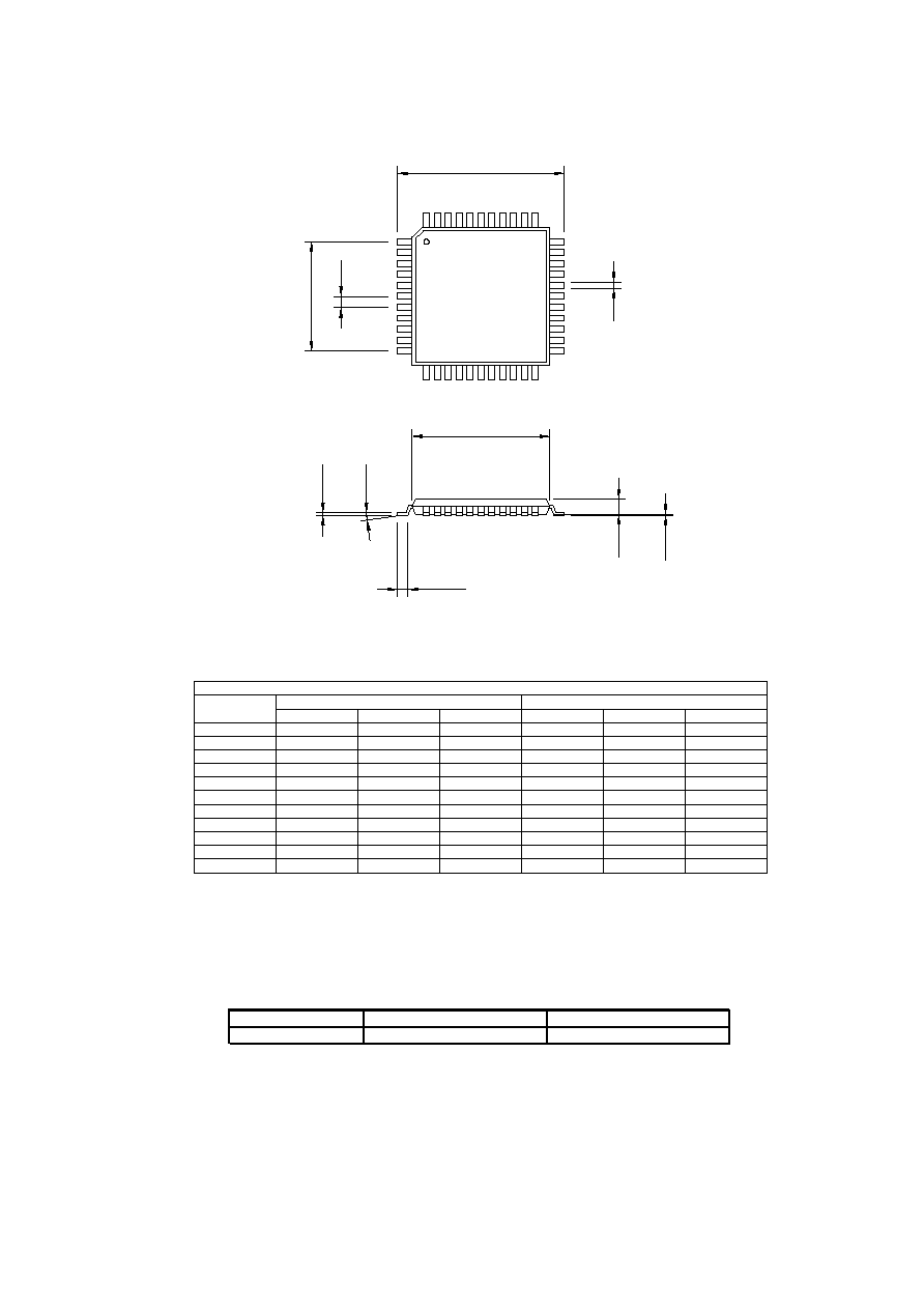
8 MECHANICAL
8.1 Dimensions
8.2 Marking
L
Q
13
QT60320D R1.11/12.07.03
1
2
3
4
8
7
6
5
11
10
9
33
32
31
30
28
23
24
25
26
27
29
12
14
16
18
22
20
15
17
19
21
13
44
42
40
38
36
34
43
41
37
39
35
SYMBOL
A
e
E
h
H
L
p
P
a
Millimeters
Inches
Min
Max
Notes
Min
Max
Notes
E
H
h
a
e
p
A
L
o
12.21
11.75
0.458
0.478
0.09
0.20
0.003
0.008
0.45
0.05
0.75
0.15
1.20
0.018
0.002
0.030
0.006
0.047
0.80
0.30
BSC
8.00
0.80
0.45
0.031
0.012
BSC
0.315
0.031
0.018
9.90
10.10
0.386
0.394
-
-
o
0
7
0
7
P
BSC
BSC
SQ
SQ
SQ
SQ
Package Type: 44 Pin TQFP
8.00
0.315
QT60320D-A
QT60320D-AS
-40
0
C to +105
0
C
Marking
TQFP
T
A

l
Q
Copyright © 1999, 2001 QRG Ltd. All rights reserved.
Patented and patents pending
Corporate Headquarters
1 Mitchell Point
Ensign Way, Hamble SO31 4RF
Great Britain
Tel: +44 (0)23 8056 5600 Fax: +44 (0)23 8045 3939
admin@qprox.com
www.qprox.com
North America
651 Holiday Drive Bldg. 5 / 300
Pittsburgh, PA 15220 USA
Tel: 412-391-7367 Fax: 412-291-1015
The specifications set out in this document are subject to change without notice. All products sold and services supplied by QRG are subject
to our Terms and Conditions of sale and supply of services which are available online at www.qprox.com and are supplied with every order
acknowledgement. QProx, QTouch, QMatrix, QLevel, and QSlide are trademarks of QRG. QRG products are not suitable for medical
(including life-saving equipment), safety or mission critical applications or other similar purposes. Except as expressly set out in QRG's
Terms and Conditions, no licenses to patents or other intellectual property of QRG (express or implied) are granted by QRG in connection
with the sale of QRG products or provision of QRG services. QRG will not be liable for customer product design and customers are entirely
responsible for their products and applications which incorporate QRG's products.