
QuadHDTV
2003 ≠ Silicon Video, Inc. ≠ All rights reserved
PDS0026 Rev A Subject to change without notice. Page 1 of 26
Key Features
∑ High resolution
o
4 times resolution of HDTV
o
3840 X 2160 color or mono pixels
o
plus 3840 X 32 optical black pixels
o
2160i, 2160p standards
∑ High speed
o
8 ports
o
30 frames/s at 37.125MHz (progressive)
o
60 fields/sec at 37.125MHz (interlaced)
∑ High sensitivity
o
20
µV/electron
∑ High dynamic range
o
2.0-volt peak signal
∑ Ultra low FPN
o
Patented ACS
technology
∑ HDTV Image format 16:9 aspect ratio
∑ Compatible with 35mm optics
o
28.8mm by 16.44mm (incl. OB)
o
33.2mm diagonal
o
7.5
µm X 7.5µm pixel
∑ Choice of color or monochrome models
o
RGB Bayer color filter array + microlenses
o
Monochrome + microlenses
∑ Ease of application
o
5.0-volt supply voltage
o
Integrated timing controller
Single clock
Horizontal / Vertical sync signals
Simple mode bits
o
Digital I/O is CMOS/TTL compatible
∑ Programmable Gain/Offset/Exposure
o
3-wire serial interface
o
Integrated programmable video amplifiers
with independent gain and offset control
per output
o
Integrated exposure controller with
programmable exposure time
∑
Reference Design Kit available
LCC package (shown without lid)
0
1
2
483 484 485
0
1
2
483 484 485
0
1
0
1
2
2
484 485
484 485
483
483
0
1
0
1
2
2
484 485
484 485
483
483
ROW 0
ROW 31
ROW 32
ROW 33
ROW 2190
ROW 2191
PSD0026_9.vsd
3.645 mm
7.5um
7.5um
240um
Optical
Black
RGB
Figure 1. Pixel Structure Diagram, one segment
Q
u
a
dHDTV
High Resolution Color/Monochrome Video Sensor
Data Sheet
Silicon Video Inc.
P.O. Box 4902, Ithaca, NY 14852-4902,
.
TEL: 607.756.5200
,
FAX: 607.756.5319
www.siliconvideo.biz
,
sales@siliconvideo.biz

QuadHDTV
2003 ≠ Silicon Video, Inc. ≠ All rights reserved
PDS0026 Rev A Subject to change without notice. Page 2 of 26
Description
The QuadHDTV
sensor is a multimode video image sensor capable of operating in either progressive or interlaced
modes at frame rates as high as 30 fps and having a choice of monochrome or color pixels. The color sensor features
a 3840 by 2160 pixel photodiode array integrated with an RGB Bayer color filter array and microlenses. The
monochrome sensor features the same photodiode array plus microlenses but without the color filters. Accurate black
levels are available for clamping with each frame ≠ the QuadHDTV
sensor includes a 3840 by 32 optical black
pixel sub-array at the top of each frame for a total of 3840 by 2192 pixels per frame (>8.4 Mpixels per frame). The
QuadHDTV
sensor captures high quality, low noise images while consuming modest power of 2 watts typical.
Very high gain uniformity resulting in low overall fixed pattern noise (FPN) is assured with the patented Active
Column Sensor ACS
PD array. Incorporation of a patent-pending high speed video bus technology for
multiplexing the video data at an average rate of 249M-pixel per second (per output) enables the 30fps performance
without a power penalty. The QuadHDTV
sensor also features flexible timing control and exposure control along
with addressable registers for controlling video gain, video offset and exposure time. Whether projected onto a
cinema screen, broadcast, displayed on a high-resolution monitor or captured for image analysis, the resultant video
exhibits detail far greater than with previous silicon image sensor technologies.
Applications
∑ Digital Cinema
∑ Advanced HDTV Broadcast
∑ Biometrics
∑ Security / Surveillance
∑ Scientific Research
∑ Military
Table 1 - Array Data
Pixel Type
Active Column Sensor (ACS
)
Array Size
2192 rows (top 32 are optical black, remaining are RGB)
Pixel Size / Pitch
7.5
µm by 7.5 µm on 7.5 µm pitch
Fill Factor
49% actual; 64% effective with micro lens
Imaging Area
RGB sub-array: 28.8mm by 16.20mm
Optical black sub-array: 28.8mm by 0.24mm
Optical Format
35mm nominal (33.2 mm actual diagonal)
Pixel Order
Row 0 ≠ 31: Black
Row 32: Red ≠ Green ≠ Red ...
Row 33: Green ≠ Blue ≠ Green ...
Row 2190: Red ≠ Green ≠ Red ...
Row 2191: Green ≠ Blue ≠ Green ...

QuadHDTV
2003 ≠ Silicon Video, Inc. ≠ All rights reserved
PDS0026 Rev A Subject to change without notice. Page 3 of 26
Table 2 - Electro-Optical Specifications
Unless otherwise specified: T
A
= 25
∞C, AVDD = DVDD = 5 volts, CLK = 37.125MHz @ 50% duty cycle,
Z
LOAD
= 10M
|| 8pF, Gain = 0 dB, Offset = 0.0V, Exposure setting = 002h.
Parameter Symbol
Test
Conditions
Min.
Typ.
Max.
Units
Supply Voltage, Analog
AVDD
4.75
5.00
5.25
Volts
Supply Voltage, Digital
DVDD
4.75
5.00
5.25
Volts
Supply Current, Analog
I
A
225
mA
Supply Current, Digital
I
D
225
mA
Power Dissipation
Pw
2.25
watts
Logic Input, High
V
IH
3.3
Volts
Logic Input, Low
V
IL
0.8
Volts
Frequency, Pixel Clock
F
PCK
37.125
MHz
Frequency, Serial Clock
F
SCK
10.0
MHz
Output Voltage, at dark
V
DARK
0.8 Volts
Output Voltage Swing, Full Scale
[1]
V
FS
2.0
Volts
Noise, random
[2]
e
n
710
µV
rmse
Dynamic Range
[3]
DR
69
dB
Average Dark Offset
ADO
Per frame at 30fps
7.0
mV
Fixed Pattern Noise
[4]
FPN
50
mV
pp
Dark Signal shading, horiz.
DSSH
0
mV
pp
Dark Signal shading, vert.
DSSV
2.0
mV
pp
Photoresponse Nonuniformity
PRNU
50% of full well
0.71
mV
rms
Full Well Capacity
FW
80K
e
-
Conversion Gain
G
C
20
µV/e
-
Quantum Efficiency, Mono, Peak
QE
= 600 nm
64
%
Responsivity, Red, Peak
= 750 nm
9.7
V/
µJ/cm
2
Responsivity, Green, Peak
= 540 nm
7.9
V/
µJ/cm
2
Responsivity, Blue, Peak
= 490 nm
7.0
V/
µJ/cm
2
Photometric Response, Mono
[5]
R
VM
2.4
V/lx-s
Photometric Response, Red
[5]
R
VR
1.8
V/lx-s
Photometric Response, Grn
[5]
R
VG
1.4
V/lx-s
Photometric Response, Blue
[5]
R
VB
1.0
V/lx-s
Saturation Exposure, Mono
[5]
SE
M
0.83
lx-s
Saturation Exposure, Red
[5]
SE
R
1.1
lx-s
Saturation Exposure, Green
[5]
SE
G
1.4
lx-s
Saturation Exposure, Blue
[5]
SE
B
2.0
lx-s
Modulation Transfer Function
MTF
Vert. @ 50 lp/mm
50
%
Image lag
IL
TBD
%V
FS
Linearity, per segment
[6]
L
1%-75% of V
FS
98.5
%V
FS
Notes:
1. V
FS
V
SAT
- V
DARK
, where V
SAT
is the output voltage at saturation and V
DARK
is the output voltage in the dark.
Therefore, V
SAT
is 2.8 Volts when the imager gain is set to 0 dB.
2. Temporal noise, e
n
measured at dark w/30MHz video filter applied and imager gain set to 0dB.
3. DR
V
FS
/ e
n
.
4. FPN is also commonly referred to as dark signal nonuniformity (DSNU).
5. Measured at 3000K and 16 Lux using Schott BG-38 IR Cut filter
6. L
(1 ≠ E
pp
/V
FS
)*100% where E
pp
is the peak to peak deviation of the response to a `best fit' straight line
fitted to the response from 1% to 75% of full scale. Measured per output.
QuadHDTV
2003 ≠ Silicon Video, Inc. ≠ All rights reserved
PDS0026 Rev A Subject to change without notice. Page 4 of 26
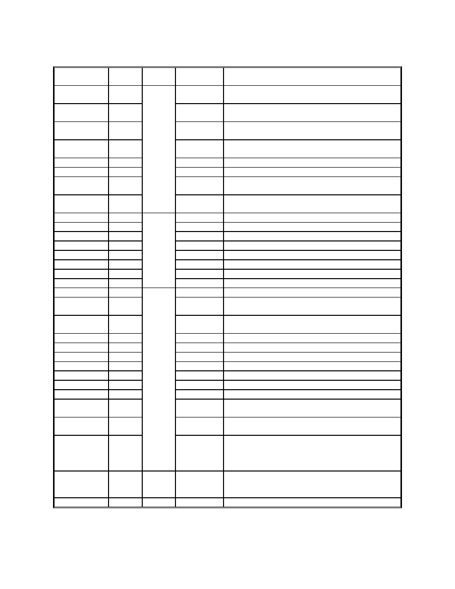
Table 3 - Signal Labels and Definitions
Signal Name
Pin
Name
Signal
Type
Pin No.
Function
Analog Supply
AVDD
4,6,18,42,47,
48,52,57
Multiple pins. Supplies 5.0-volts to the internal analog
circuitry. Bypass externally to AGND
Analog Ground
AGND
5,7,19,41,48,
51,58
Multiple pins. Distributes common ground node
(0-volts) to the internal analog circuitry.
Digital Supply
DVDD
15,26,44,54,
63
Multiple pins. Supplies 5.0-volts to the internal digital
circuitry. Bypass externally to DGND
Digital Ground
DGND
16,27,45,55,
64
Multiple pins. Distributes common ground node
(0-volts) to the internal digital circuitry.
Guard Bias
PVDD
11,12,22,23
Multiple pins. Pixel array guard ring bias.
Guard Ground
PGND
9,10,20,21
Multiple pins. Pixel array guard ring bias return.
Pixel Supply
PDBIAS
1,32
Multiple pins. Internal bias voltage to pixels. Bypass
externally to AGND
Substrate
Ground
GND
Bias
13,14
Multiple pins. Backside of sensor chip.
Chan 0 O/P
A0
59
Single-ended video output ≠ leftmost 486 columns
Chan 1 O/P
A1
56
Single-ended video output ≠ 486 columns
Chan 2 O/P
A2
53
Single-ended video output ≠ 486 columns
Chan 3 O/P
A3
50
Single-ended video output ≠ 486 columns
Chan 4 O/P
A4
49
Single-ended video output ≠ 486 columns
Chan 5 O/P
A5
46
Single-ended video output ≠ 486 columns
Chan 6 O/P
A6
43
Single-ended video output ≠ 486 columns
Chan 7 O/P
A7
Video
Outputs
40
Single-ended video output ≠ rightmost 486 columns
Clock
CLK
35
Master clock input. Nominally 50% duty cycle
System Reset
RESET
30
Asynchronous system logic reset. Clears programmable
registers.
Global Pixel
Reset
GPR
25
Asynchronous global reset of the pixel array
Horiz. sync
HD
37
Low active input signals start of line
Vertical sync
VD
36
Low active input signals start of frame
Field select
O/E
33
High = Even field, Low = Odd field (Interlaced scan)
Scan mode
P/I
31
High = Progressive, Low = Interlaced
Serial clock
SCLK
62
10 MHz max. for serial data transfer
Serial enable
SEN
60
Low active input indicates valid message for device
Serial data
SDATA
61
Internal serial register address followed by data
External
exposure sync
EXTEXP
34
High active input triggers exposure when operated in
long (multi-frame) exposure mode. (E-shutter)
Test mode
enable
TEST
29
Overrides scan mode and places imager in test mode.
High = TEST mode, Low = Normal modes.
Test line select
TS[1:0]
Digital
Inputs
39, 38
TS[1:0] = 00 test mode readout starts at line 0
TS[1:0] = 01 test mode readout starts at line 832
TS[1:0] = 10 test mode readout starts at line 1712
TS[1:0] = 11 (reserved)
Frame enable
FENB
Digital
output
28
High active output acts as a `frame data valid' signal
when operated in long (multi-frame) exposure mode.
Always HIGH when short shutter mode is selected.
No connection
NC
2,3,8,17,24

QuadHDTV
2003 ≠ Silicon Video, Inc. ≠ All rights reserved
PDS0026 Rev A Subject to change without notice. Page 5 of 26
Figure 2 - Pin-out diagram, top view
Absolute Maximum Specifications
Supply voltage range, V
DD
[1]
......................................................................
0 V to 7 V
Digital input current range, I
IN
....................................................................
≠5 mA to 5 mA
Digital output current range, I
OUT
................................................................
Exceeding the ranges specified under "absolute maximum ratings" can damage the device. The values given are for stress ratings only.
Operation of the device at conditions other than those indicated above, is not implied. Exposing the device to absolute maximum rated
conditions for extended periods may affect device reliability and performance.
Notes:
1. Voltage values are with respect to the device GND terminal.
Environmental Specifications
Operating case temperature range, T
CASE
[1]
.................................................
≠10∞C to 55∞C
Storage temperature range......................................................................
≠20∞C to 85∞C
Humidity range, R
H
................................................................................. 0-100%,
non-condensing
Solder reflow temperature for 10 seconds max.............................................
225∞C
PDBIAS
NC
NC
AVDD
AGND
AVDD
AGND
NC
PGND
PGND
PVDD
PVDD
GND
GND
DVDD
DGND
NC
AVDD
AGND
PGND
PGND
PVDD
PVDD
NC
GPR
DVDD
DGND
FENB
TEST
RESET
P/I
PDBIAS
1
2
3
4
5
6
7
8
9
10
11
12
13
14
15
16
17
18
19
20
21
22
23
24
25
26
27
28
29
30
31
32
DGND
DVDD
SCLK
SDATA
SEN
A0
AGND
AVDD
A1
DGND
DVDD
A2
AVDD
AGND
A3
A4
AGND
AVDD
A5
DGND
DVDD
A6
AVDD
AGND
A7
TS[1]
TS[0]
HD
VD
CLK
EXTEXP
E/O
64
63
62
61
60
59
58
57
56
55
54
53
52
51
50
49
48
47
46
45
44
43
42
41
40
39
38
37
36
35
34
33
TO
P
O
F
FR
A
M
E
QuadHDTV
Top View

QuadHDTV
2003 ≠ Silicon Video, Inc. ≠ All rights reserved
PDS0026 Rev A Subject to change without notice. Page 6 of 26
0.0
0.1
0.2
0.3
0.4
0.5
0.6
0.7
0.8
0.9
1.0
380
430
480
530
580
630
680
730
Wavelength (nm)
Relative Response
Red
Green
Blue
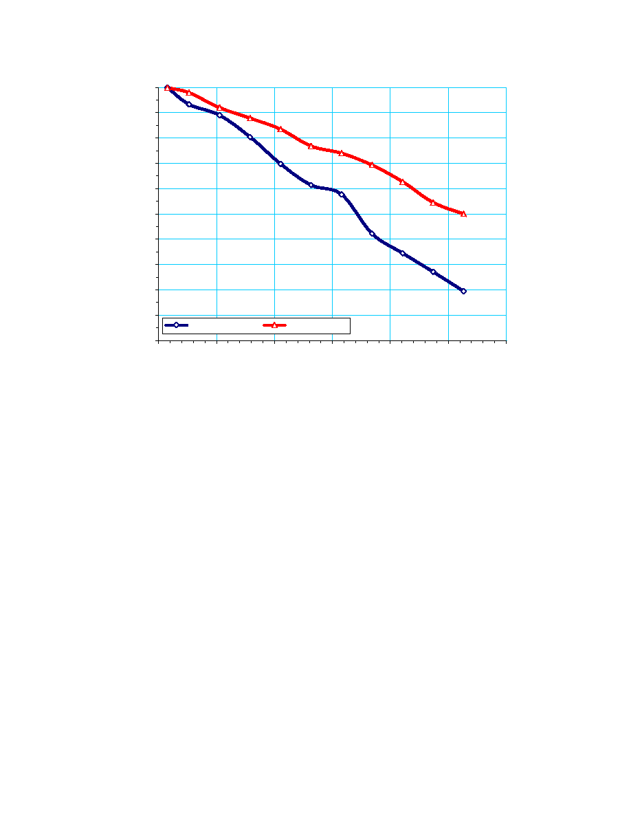
Figure 3 ≠ Relative Responsivity (color model)
0%
10%
20%
30%
40%
50%
60%
70%
400
500
600
700
800
900
Wavelength (nm)
Quantum Efficiency (%)
Figure 4. Quantum efficiency vs. wavelength (monochrome model)
QuadHDTV
2003 ≠ Silicon Video, Inc. ≠ All rights reserved
PDS0026 Rev A Subject to change without notice. Page 7 of 26
0.0
0.1
0.2
0.3
0.4
0.5
0.6
0.7
0.8
0.9
1.0
0
10
20
30
40
50
60
Spatial Frequency (lp/mm)
MTF
Horizontal MTF
Vertical MTF
Figure 5. Measured MTF (monochrome model)
QuadHDTV
2003 ≠ Silicon Video, Inc. ≠ All rights reserved
PDS0026 Rev A Subject to change without notice. Page 8 of 26
Application Data
486
column
ACS
TM
and
CDS
PGA
A0
PGA
A1
PGA
A2
PGA
A3
PGA
A4
PGA
A5
PGA
A6
PGA
A7
R
o
w
C
o
n
t
r
o
l fo
r
s
e
le
c
t
io
n
and res
e
t
2192
486
column
ACS
TM
and
CDS
486
column
ACS
TM
and
CDS
486
column
ACS
TM
and
CDS
486
column
ACS
TM
and
CDS
486
column
ACS
TM
and
CDS
486
column
ACS
TM
and
CDS
486
column
ACS
TM
and
CDS
486
column
PVS-
Bus
TM
486
column
PVS-
Bus
TM
486
column
PVS-
Bus
TM
486
column
PVS-
Bus
TM
486
column
PVS-
Bus
TM
486
column
PVS-
Bus
TM
486
column
PVS-
Bus
TM
486
column
PVS-
Bus
TM
3 Wire
Serial
Interface
16
Exposure
Controller
16
Ref
e
renc
e Gener
at
or f
o
r
PD
Ar
r
a
y
FENB
SCLK
SEN
SDATA
PDBIAS
Timing Controller
HD
VD
CL
K
P/I E/O
TEST
EXTEXP
3840 X 2160 Pixel
ACS
TM
Photodiode Array
TS[1
:0]
2
TOP OF FRAME
HORIZONTAL SCAN
VER
TIC
A
L
SC
AN
PDS0026_1.vsd
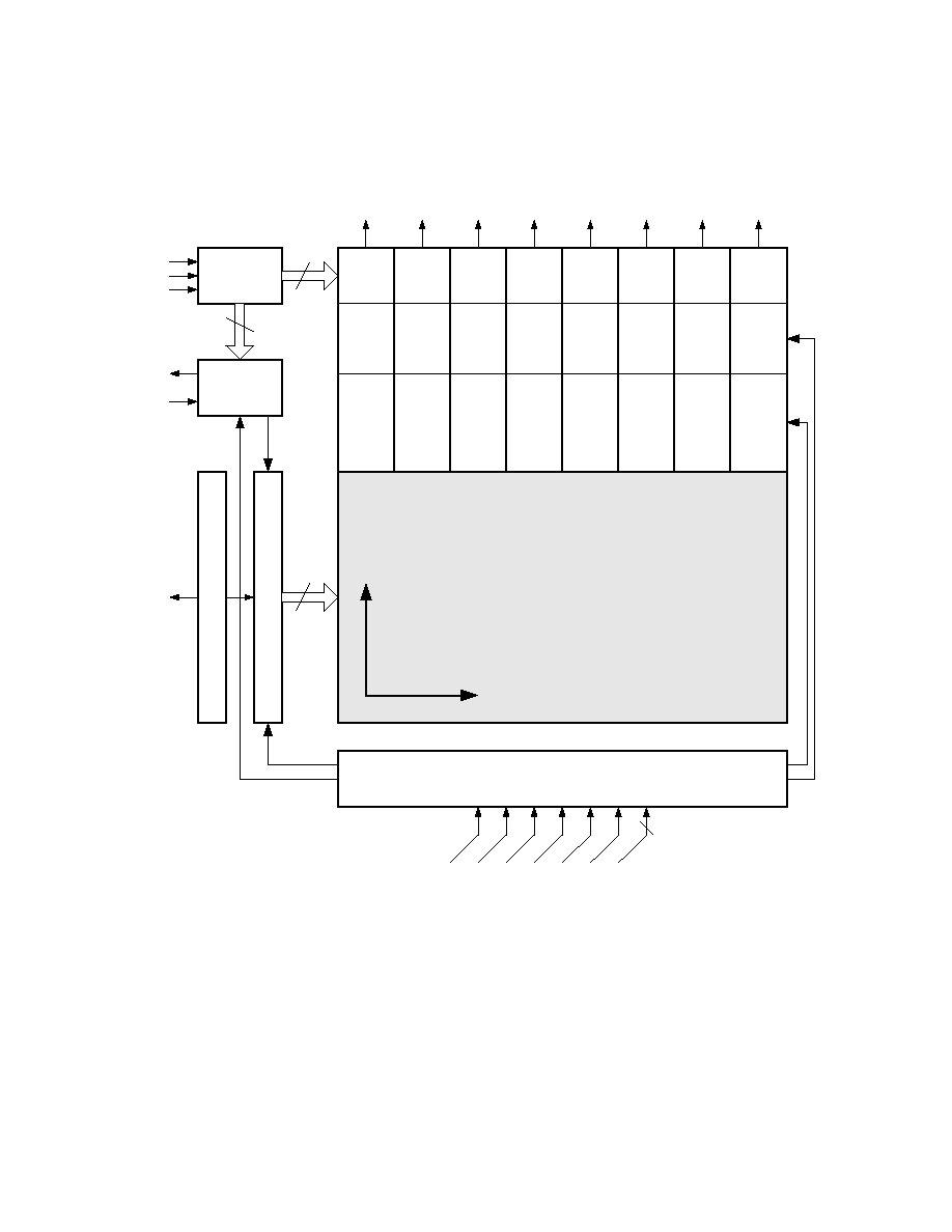
Figure 6 - Simplified Block Diagram
QuadHDTV
2003 ≠ Silicon Video, Inc. ≠ All rights reserved
PDS0026 Rev A Subject to change without notice. Page 9 of 26
Theory of Operation
Overview
A simplified functional block diagram of the
QuadHDTV
imager is shown in Figure 6. Each of
the eight video outputs represents 486 columns of the
3888 total columns of pixels with each column of the
pixel array consisting of 2192 pixels. Thus each
output represents more than 1 million pixels
(1,065,312). Each column of pixels is processed by
the patented ACS
technology pixel multiplexer,
which is followed by a correlated double sampler
(CDS) circuit that produces samples of both the
integrated photodiode voltage (video) and the
photodiode reset voltage (background). The patent-
pending video bus technology is used as a dual, high-
speed 486:1 multiplexer to deliver the video and reset
voltages to the output amplifier differentially. The
output video amplifier subtracts the video voltage
from the reset voltage to yield a positive going video
signal that is corrected for pixel reset-related offsets.
The output video amplifier can subtract an offset of
as much as 765mV from the video signal and then
apply a gain from 0 to +12 dB. Both the offset and
gain are under user control via the 3-wire serial
interface. The row controllers are used to select and
reset rows of pixels in a sequential manner thereby
implementing a rolling-shutter exposure system. It is
also possible to reset the entire array of pixels at once
using the Global pixel reset (GPR) input. The
integrated exposure controller provides two exposure
modes: short mode and long mode. In short mode
exposure time is varied linearly from 100% of the
frame-time down to less than 1% of the frame-time.
In long mode, exposure time is varied from 1 frame-
time per image frame to 4095 frame-times per image
frame. The pixels are reset to an internally generated
bias voltage, PDBIAS, which is brought out to two
package pins for external decoupling. The integrated
timing controller is the master timer for the imager
and ensures that row and column events occur at the
proper times in addition to synchronizing with the
exposure controller. For the most part, the user
determines frame rate, pixel rate, etc. by providing a
pixel clock, a horizontal sync pulse and a vertical
sync pulse. P/I is used to determine whether to
operate in progressive or interlaced scan modes. The
E/O input is used in interlaced mode to establish
which field is even/odd. By definition, E/O must be
set to EVEN for progressive mode. The TEST input
overrides the P/I input and puts the imager in Test
mode. When in Test mode, TS[1:0] are active for
selecting which portion of the pixel array to read out.
A survey of design and testing of the imager can be
found in Ref. [5].
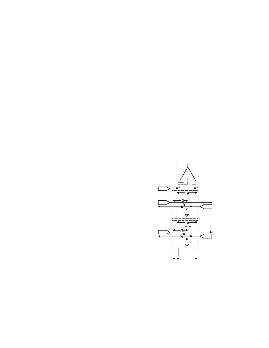
Active Column Sensor ACS
The SVI-exclusive Active Column Sensor technology
(ACS
) provides video signals that are inherently
free of fixed pattern noise caused by gain and offset
of pixel amplifiers. Rather than using an independent,
open loop source follower amplifier per pixel like
APS imagers do, the ACS
technique uses a single,
closed loop unity gain amplifier (UGA) that is shared
among all of the pixels in a column. Thus, each pixel
has a virtual closed-loop amplifier, that is, each pixel
in a column behaves as if it has its own closed-loop
UGA but having identically the same gain and offset.
Since all of the columns employ closed-loop UGA's,
the gain uniformity from column to column is also
exceedingly high. The correlated double-sampling
circuit that follows each UGA removes UGA offset.
The result is a dramatically low FPN especially when
compared to uncorrected APS imagers. The
simplified ACS schematic diagram below shows two
pixels connected to the column UGA. For more
details of the ACS technology see references [1- 3].
RESET 'N'
UGA
D
SELECT 'N'
RESET 'N+1'
SELECT 'N+1'
PDBIAS
to o
t
her
pi
xel
s
PD
RESET
D
S
to other
columns
to other
columns
PD
RESET
D
S
to other
columns
to other
columns
to o
t
her
pi
xel
s
PDS0026_8.vsd
Video Bus multiplexer
The Video Bus multiplexer is a patent-pending high
speed, low power switch array ideally suited to dense
area arrays like the QuadHDTV
imager.
Multiplexers for large arrays must contend with high
capacitance, due to a large number of switches, and
high switching rate, which is required to read out the

QuadHDTV
2003 ≠ Silicon Video, Inc. ≠ All rights reserved
PDS0026 Rev A Subject to change without notice. Page 10 of 26
entire array in the available frame time. This is
readily recognized as a fundamental application of:
dt
dV
C
t
i
=
)
(
(1)
Clearly, using a brute force approach requires high
instantaneous current to charge and discharge a large
capacitance at high pixel rates. Rather than
multiplexing directly from N:1 (in this case 486:1),
the Video Bus utilizes a two-tiered architecture ≠
multiplex from N:M first and then from M:1. In the
case of the QuadHDTV
imager, the Video Bus is
realized as a 486:16 multiplexer followed by a 16:1
multiplexer, thus M=16. This approach has the virtue
of reducing the capacitance `C' by a factor of M and
multiplying the available charging time `dt' by a
factor of M for an overall charging current reduction
of M
2
. A more detailed discussion of the Video Bus
architecture can be found in reference [4].
Rolling shutter
The QuadHDTV
imager provides a rolling shutter
architecture to maximize the available pixel area for
light collection. The rolling shutter in a CMOS image
sensor works analogously to a focal plane shutter in a
film camera, which is why the rolling shutter is
sometimes referred to as an electronic focal plane
shutter. The rows of pixels in the image sensor are
reset in sequence, starting at the top of the image and
proceeding row by row to the bottom. When this reset
process has moved some distance down the image,
the readout process begins. Rows of pixels are read
out in sequence, starting at the top of the image and
proceeding row by row to the bottom in exactly the
same fashion and at the same speed as the reset
process.
The rolling shutter exposure method differs from the
snap-shot exposure method. A snap-shot exposure
refers to the method wherein all pixels are exposed to
light for the same duration and at exactly the same
time i.e. light integration starts and ends at identically
the same time. Rolling shutter exposure refers to the
method wherein all pixels are exposed to light for the
same duration but each row of pixels starts and ends
at a slightly different time. Thus both methods will
yield the same light integration duration but will
differ in the exposure start/stop times of rows of
pixels.
In progressive scan mode, the lines are read out in
sequential order starting with line 0 through line 2192
meaning that the pixel integration period for each line
is offset from the preceding line by exactly one line-
time or about 14.8
µs when operating at 30fps. In
interlaced scan mode, the even-numbered lines are
read out first followed by the odd-numbered lines.
Device Operation and Timing
General
The QuadHDTV
imager features four times the
spatial resolution required for HDTV, which, when
used for HDTV applications, permits accurate color
separation per pixel without interpolation. This is
possible because an imager with only 1X HDTV
resolution must approximate a color assignment for
every pixel based on the color information of it's
neighbors, whereas the QuadHDTV
imager
contains complete RGB color information per HDTV
pixel i.e. per four-pixel quad. Thus no interpolation is
required and more accurate color rendition results.
For non-HDTV applications, which require the 4X
HDTV resolution of the QuadHDTV
imager, the
option to interpolate colors always remains. In
addition to the image pixels, 32 rows of optical black
pixels are included to permit accurate system
calibration to the sensor's black level.
High video bandwidth is assured by the proprietary
Video Bus multiplexer technology. The
QuadHDTV
achieves 30 frames/s using only eight
ports when operating with a system clock of
37.125MHz. This corresponds to 32 million image
pixels per second per output port or a total of 256
million image pixels per second.
Pixel sensitivity and dynamic range remain high due
to the overall pixel design, the ACS
pixel
multiplexer and the use of microlenses. Typical
conversion efficiency is 20
µV/electron with a
dynamic range of better than 58dB. A standard RGB
Bayer color filter array is also included. The image
aspect ratio is standard HDTV 16:9 with a diagonal
of 33.2 mm making the imager compatible with
35mm optics for ease of optical application.
Ease of application is further enhanced by the
inclusion of an integrated timing controller, an
integrated exposure controller, single 5-volt supply
voltage operation and digital I/O that is CMOS/TTL
compatible. The integrated timing controller only
requires a single non-critical pixel clock (at the
desired pixel rate), horizontal and vertical sync
signals and two mode bits for controlling progressive
and interlaced modes. A Test mode is included for

QuadHDTV
2003 ≠ Silicon Video, Inc. ≠ All rights reserved
PDS0026 Rev A Subject to change without notice. Page 11 of 26
viewing user selectable portions of the pixel array
with a VGA-monitor.
Each of the eight output video amplifiers features
programmable gain and offset that can be set using a
simple 3-wire serial interface. Gain can be varied
from 0 to +12dB, offset can be varied from 0.8-volts
to less than 100mV. Both gain and offset settings
have 8-bit resolution. The serial interface is also used
to set exposure modes (short mode vs. long mode)
and exposure time. In short exposure mode, exposure
time can be varied from 100% to less than 1% with
12-bit resolution.
Controlling the imager
The QuadHDTV
imager requires five timing signals
to produce proper video in the normal scan modes ≠
CLK, VD, HD, P/I and O/E. CLK is the clock input
to the imager and may be TTL or 5V CMOS
compatible. For proper HDTV operation the clock
frequency must be 37.125 MHz. VD and HD are the
vertical and horizontal sync pulses respectively ≠ the
timing between them is given in Figure 7. In the
figure, H is the period of a horizontal line, which
should be exactly 550 clock cycles (T). The period of
VD should be exactly 2250H to achieve 30 frames/s.
Figure 7. VD / HD timing (start of frame)
VD goes low at the start of each frame and remains
low for exactly one line time (1H). HD goes low at
the start of each line and remains low for exactly two
clock cycles (2T) as shown in Figure 8.
Figure 8. CLK / HD timing (start of line)
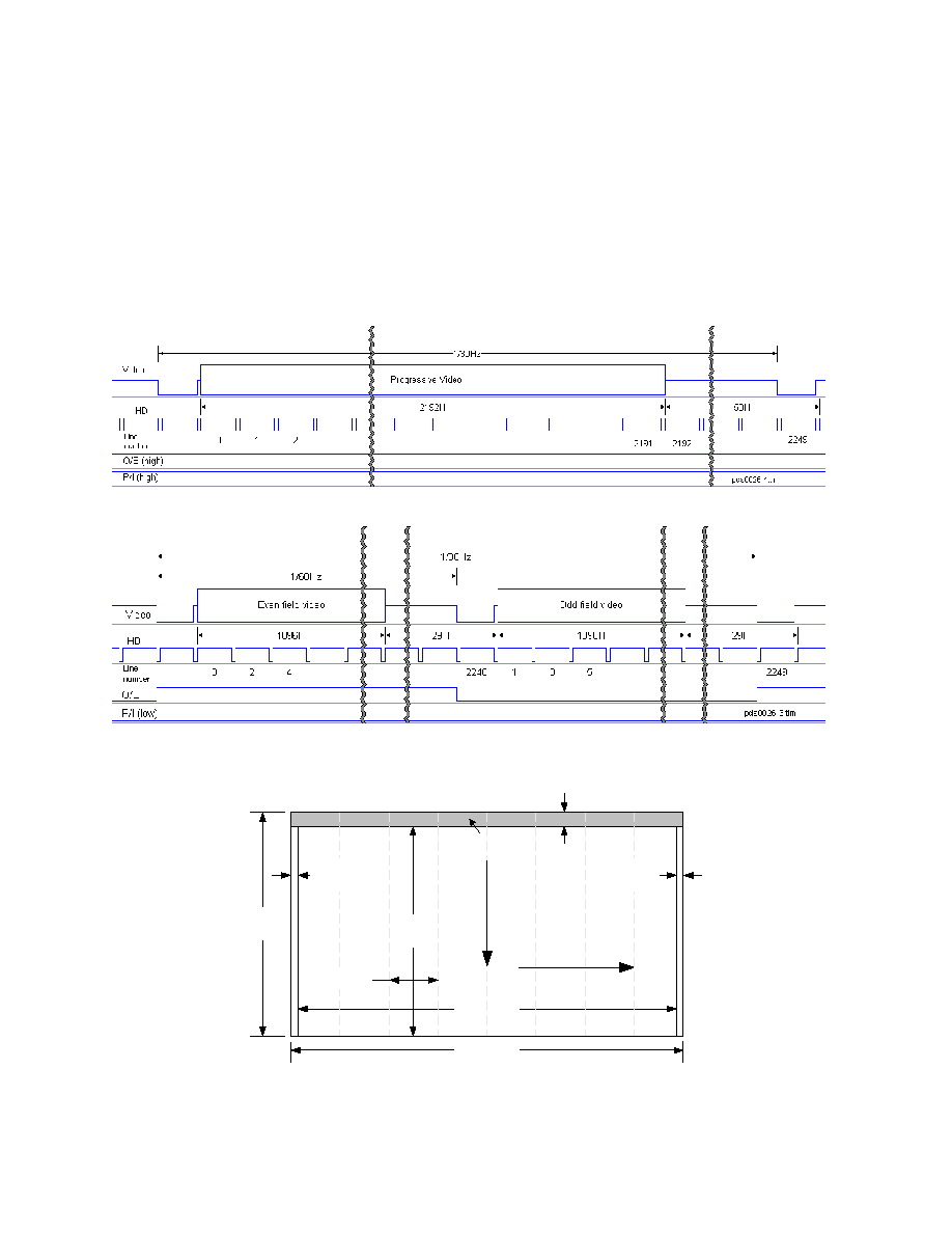
P/I is used to set the scan mode: for P/I = HIGH,
progressive scan mode is selected; for P/I = LOW,
interlaced scan mode is selected. O/E is used to
define the odd/even fields in interlaced mode. For
O/E = HIGH, the field is even, for O/E = LOW, the
field is odd. In progressive mode, O/E must remain
HIGH. See Figure 11 and Figure 12 for timing
diagrams of progressive and interlaced scan modes.
Each line (H) of video is 550T long with active video
beginning at the start of the 65
th
clock cycle following
the rising edge of HD as shown in Figure 9 below.
Figure 9. Video timing relative to HD
The detailed timing relationship between the analog
video and the CLK input is shown in Figure 10 with
values provided in Table 4. We recommend that CLK
be set to 50% duty cycle although the imager will
operate with duty cycles between 37% and 63%.
90%
10%
FS
1/2 FS
0
CLK
ANALOG
OUTPUT
(A0~A7)
Tpw1
Tpw0
Tr
Tf
Tpd
pds0026_3.vsd
Figure 10. Video timing relative to CLK
Table 4. CLK-to-Video timing values
Parameter Value
T
pw1
10ns
min.
T
pw0
10ns
min.
T
r
12ns
typ.
T
f
12ns
typ.
T
pd
TBD
Frame format
For nominal HDTV operation at 30 frames/s, the
period of VD should be set to 2250H for progressive
scan mode and 1125H for interlaced scan mode. See
Figure 11 and Figure 12. Note that for interlaced
mode there are two VD pulses per frame (one per
field). Each line should be set to 550T where
T=1/37.125MHz.
For applications other than HDTV, the periods of VD
and HD may be changed but, to ensure that all lines
and all pixels are read out, VD should not be any
shorter than 2192H and HD should not be any shorter
QuadHDTV
2003 ≠ Silicon Video, Inc. ≠ All rights reserved
PDS0026 Rev A Subject to change without notice. Page 12 of 26
than 550T. The total number of pixels in the array
exceeds the nominal 3840H by 2160V. In fact, the
pixel array measures 3888 pixels horizontally by
2192 pixels vertically.
The additional 32 vertical pixels comprise 32 optical
black (OB) rows appearing at the top of the frame
that may be utilized to establish a system black level.
During readout these OB lines are the first 32 lines
following the VD pulse in progressive mode or the
first 16 lines following each of the VD pulses in the
interlaced mode.
The additional 48 horizontal pixels may be allocated
as desired since they do not comprise OB columns.
We recommend that the first 24 pixels of each A0
video line and the last 24 pixels of each A7 video line
be ignored or used to compensate for image
misalignment in the horizontal axis. A map of the
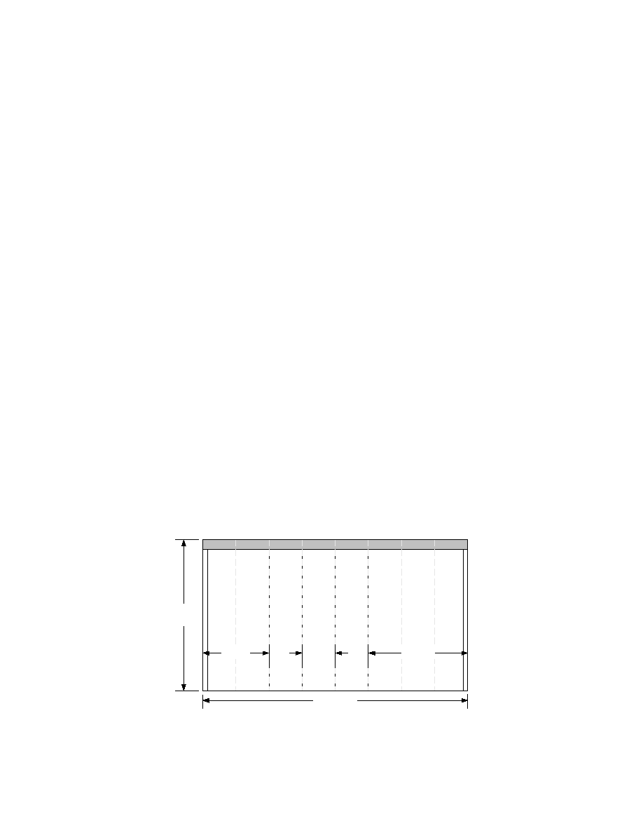
pixel array is given in Figure 13.
Figure 11. Progressive timing
Figure 12. Interlaced timing
3840 Pixels
3888 Pixels
2192
Pixels
2160
Pixels
Top of Frame
Bottom of Frame
24
Pixels
32
Pixels
Ve
rt
i
c
a
l
Scan
Dir
ec
t
i
on
Horizontal
Scan Direction
24
Pixels
PDS0026_4.vsd
A0
A7
486 Pixels
Optical black rows
Figure 13. Pixel Map
QuadHDTV
2003 ≠ Silicon Video, Inc. ≠ All rights reserved
PDS0026 Rev A Subject to change without notice. Page 13 of 26
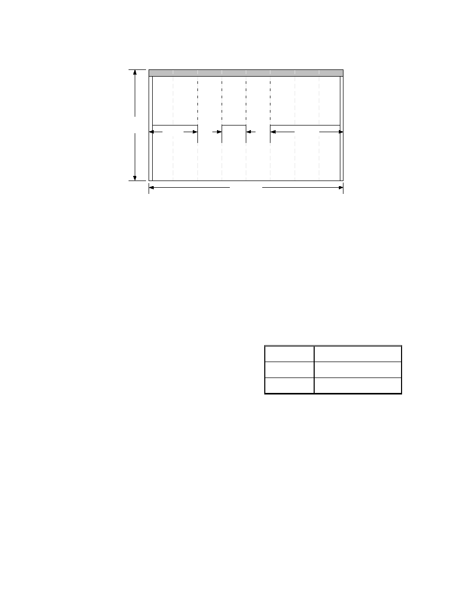
Regions of Interest
The QuadHDTV imager was not expressly designed
to accommodate user-selected regions of interest
(ROI) however limited ROI selection is possible.
Horizontally, an ROI can be defined by choosing to
use data from less than all of the outputs resulting in
horizontal ROI boundaries that fall on 486 column
increments i.e. 0, 486, 972 etc. (The choice to read or
not read a particular video output is determined
external to the sensor e.g. not reading the ADC output
for that segment.) These horizontal boundaries don't
provide any read out rate benefit though as the HD
period i.e. line time, must remain at least 550T to
ensure that all columns of each complete desired
segment are read out. That is, unless the desired ROI
is less than 486 columns wide, the HD period should
remain at full length and consequently, using less than
all eight segments will not allow you to read out the
ROI at a higher frame rate. The exception occurs
when the ROI is less than 486 columns wide and falls
within one segment ≠ the HD period can be reduced,
however, the read out of that segment will always
begin at the first column of that segment. In the case
where the ROI is less than one segment wide, the HD
period (H) must be H = 64T + nT where `n' is the
rightmost column (with reference to Figure 13) of the
segment to be read out and 64T is the required
horizontal overhead time. For example, if the desired
ROI is 300 columns wide but ends at the rightmost
edge of the segment it will still be necessary to
maintain the full HD period (550T). Conversely, in
the example above, if the ROI is 300 columns wide
and starts at the leftmost edge of the segment, then
the HD period could be set at 364T. An ROI that
crosses a segment boundary will require that both
segments be read out. In all cases, the width of the
HD pulse should always be 2T as shown in Figure 8.
See Figure 14 for a depiction of several typical ROI's
that can be easily realized simply by choosing to read
out less than all of the video outputs. Note that the
time required to read out each of the ROI's depicted
in this figure is the same as is required to read out the
entire 8.3Mpixel image. Multiple ROI's of this sort
can be read out simultaneously.
The situation with vertical ROI boundaries is a little
different in that reducing the vertical sync (VD)
period will increase frame rate. However, the first
line of every frame will always be the first optical
black row i.e. the top of the frame. Therefore, to gain
the maximum frame rate advantage when reducing the
vertical size of the ROI, it is best to align the top of
the ROI with the top of the frame. The video line data
immediately following the VD pulse low-to-high
transition corresponds to the first optical black row
(Row 0). To create an ROI whose vertical height is
half of the array maximum and whose top is aligned
with the top of the frame, T
VD
= 32H + 1080H =
1112H where H is the line time in pixel clocks. For
example, if H = 550T and T = 1/37.125MHz, then the
frame time is about 16.5ms which corresponds to
60.7Hz. This frame rate is valid whether the ROI's
horizontal extent is one segment or eight segments.
When working with ROI's whose vertical extent is
less than the full frame height, the imager should be
operated in progressive mode. Exposure control may
be used with ROI's however a slight intensity artifact
may occur when the period of VD is less than 2192H.
3/8 area ROI
1/8
area
ROI
1/4 area
ROI
3888 Pixels
2192
Pixels
Top of Frame
Bottom of Frame
PDS0026_10.vsd
A0
A7
972 col
486 col
1458 col
Figure 14. Examples of ROI's based on choosing to read out selected video outputs.
QuadHDTV
2003 ≠ Silicon Video, Inc. ≠ All rights reserved
PDS0026 Rev A Subject to change without notice. Page 14 of 26
3/16 area ROI
1/16
area
ROI
1/8 area
ROI
3888 Pixels
2192
Pixels
Top of Frame
Bottom of Frame
PDS0026_11.vsd
A0
A7
972 col
486 col
1458 col
Figure 15. Examples of ROI's based on reduction of VD period and selection of less than all video outputs.
An alternative method of realizing a variety of ROI's
that confer frame rate advantages is to utilize the Test
mode described below. The test mode ROI's are
VGA compatible, 60Hz frame rate `windows' when
operated at 37.125MHz. However, their horizontal
and vertical dimensions as well as their positions in
the overall array are fixed. By multiplexing the video
outputs of adjacent segments appropriately, each test
mode ROI will be 480(V) by 972(H). The top of each
ROI may be selected to start at row 0 (top of frame),
row 832 (mid-frame) or row 1712 (bottom of frame).
Serial Communication
The QuadHDTV
imager uses 3-wire serial
communication to load internal registers that control
exposure mode, exposure time, and voltage gain and
offset for each of the eight video output ports. The
timing of each of the three signals (SCLK, SEN,
SDATA) that comprise the serial message is the same
in all cases and is shown in Figure 16 below. The
maximum rated frequency for SCLK is 10MHz. All
SEN and SDATA transitions should be synchronous
with the falling edge of SCLK. The format of the
message's data field differs depending on whether an
exposure control message or an output amplifier
message is being sent. The data to be sent on the
SDATA line consists of a 6-bit address field, a 2-bit
spacer field, a 16-bit data field and a final 1-bit stop
field in this order. Thus, all serial messages always
require 25 clock cycles. The data field format for an
Output Amplifier Message is given in Figure 17. The
data field format for an Exposure Control Message is
given in Figure 18. Note that in the figure, the term
`
SYNC PULSE
' refers to the HD signal in short
exposure mode and to the VD signal in long exposure
mode. For the case of long exposure mode and
interlaced scan mode, `
SYNC PULSE
' refers to the
`EVEN VD' pulse of each frame. The register
addresses are given in Table 5.
Table 5. Serial Register Addresses
Address Register
00h Exposure
Control
01h-08h
Output Amplifier A0~A7
QuadHDTV
2003 ≠ Silicon Video, Inc. ≠ All rights reserved
PDS0026 Rev A Subject to change without notice. Page 15 of 26
Figure 16. 3-wire Serial Message Timing
D15
D14
D13
D12
D11
D10
D9
D8
D7
D6
D5
D4
D3
D2
D1
D0
OFFSET
GAIN
D15-D8
OFFSET
00h
80h
FFh
D7-D0
GAIN
00h
80h
FFh
0 mV
384 mV
765 mV
1.00 V/V
2.51 V/V
4.00 V/V
pds0026_5.vsd
Figure 17. Format of Data Field of Output Amplifier Message
D15
D14
D13
D12
D11
D10
D9
D8
D7
D6
D5
D4
D3
D2
D1
D0
Exposure Mode
Exposure Delay
D15
MODE
0
1
D11-D0
EXPOSURE DELAY
000h
FFFh
SHORT
LONG
0 X SYNC PULSE
4095 X SYNC PULSE
pds0026_6.vsd
RESERVED
Figure 18. Format of Data Field of Exposure Control Message
Offset and Gain Control
Each video port accepts a byte for offset (D[15:8])
and a byte for gain (D[7:0]). Thus, there are 256
possible gain settings and 256 possible offset
subtraction settings that can be programmed for each
video output stage. Default operation is gain equal to
1.0 and no offset subtraction. See Figure 19 for a
simplified block diagram of the video output stage.
V
REF
is nominally 1.0 volt, thus if the programmed
offset is 00h (no offset) the output d.c. level will be
equal to V
REF
. Programmed offsets are subtracted
from V
REF
and have the effect of reducing the d.c.
voltage at the video output port. The `offset' LSB is
set at a nominal value of 3.0 millivolts of video
offset; the full-scale offset reduction is 765 millivolts.
To compute the actual offset setting corresponding to
a given gain code use the following formula:
]
[
0
.
3
code
mV
Vref
Offset
◊
-
=
(2)
The output video amplifier operates at a fixed gain of
about 4.5 V/V and is preceded by an 8-bit linear
programmable attenuator. Thus, unity gain operation
is achieved by first attenuating the signal and then
applying a fixed gain. The advantage of using this
topology is that bandwidth and noise are not
functions of the gain setting and amplifier stability is
assured at all gain settings. The output video gain is a
linear function of the programmed value with 00h
corresponding to unity gain and FFh corresponding to
a closed loop gain of 4.0. Each `gain' LSB produces a
gain increase of about .018 V/V (3
˜ 255). To

QuadHDTV
2003 ≠ Silicon Video, Inc. ≠ All rights reserved
PDS0026 Rev A Subject to change without notice. Page 16 of 26
compute the actual gain setting corresponding to a
given gain code use the following formula:
1
255
]
[
3
+
◊
=
code
Gain
(3)
The video output voltage is positive going starting
from the d.c. offset level. At unity gain the output
voltage range is about 1 volt for all offset settings. At
a gain of 4.0, the output voltage range may swing
from as low as about 0.3 V (dark) to as high as 3.5
volts (saturation), due to an internal voltage
limitation.
V
IN
V
BLACK
R
ATT
OFF
3.5 R
R
R
R
R
V
OUT
V
REF
DATA BUS
16
8
8
PDS0026_7.vsd
Figure 19. Output Video Stage, Simplified Block Diagram
Exposure Control
The QuadHDTV
imager has two exposure modes:
short exposure and long exposure, both of which may
be used with either progressive or interlaced scan
modes. (The TEST scan mode does not provide any
means for varying exposure ≠ it always operates with
a full frame-time of exposure.) The short exposure
mode permits the imager to produce frames at the
maximum rate, typically 30 fps, and vary the
integration time from a full frame time (1/30
th
of a
second) down to one line time (about 15
µs) in
increments of one line time. Integration time
resolution is thus 0.044% (1
˜2250) allowing for very
fine control of exposure.
The long exposure mode allows exposures greater
than one frame-time up to 4095 frame-times in
increments of 1 frame-time. When operating with a
37.125MHz clock, this corresponds to a maximum
exposure of 136 seconds in increments of 1/30
th
of a
second. The long exposure mode also features an
external trigger input, EXTEXP that permits
synchronization of the output video to external
events. See Figure 20 for a diagram of the EXTEXP
timing requirements. For both long and short
exposure modes, changes in exposure mode or
exposure duration (integration time) take effect on the
next full frame of exposure.
Short exposure is set by making bit D15 equal to 0,
allowing the bits D[11:0] to be interpreted as the
number of line times to delay from the start of the
frame before starting the next exposure where the
start of the frame is defined by the appearance of the
VD pulse
1
. (For interlaced mode, the start of the
frame is defined by the appearance of the VD pulse in
the EVEN field.) Short exposure mode always
reduces the integration time from the maximum value,
which is one frame-time. The general expression for
determining the integration time is:
1
Technically, since the QuadHDTV imager uses a rolling-
shutter, the integration period for each line begins with
the selection of that line for read-out, as does the delay
before integration of each line. Likewise, the end of
integration for any given line is the line-time just before
its selection for read-out. Thus, only for line 0 is it
accurate to say that the integration period starts at the
beginning of the frame and continues until the end of the
frame. Nonetheless, it is convenient to think of the
exposure as always starting and ending at the frame start
`boundary'.
QuadHDTV
2003 ≠ Silicon Video, Inc. ≠ All rights reserved
PDS0026 Rev A Subject to change without notice. Page 17 of 26
frame
t
code
T
◊
-
=
2250
])
[
2250
(
exp
(4)
For D[11:0] = 000h, there is no delay and exposure
begins at the start of the frame and continues until the
end of the frame. For D[11:0] = 0FFh, there is a delay
of 255 line-times after the start of the frame before
exposure commences. In this example, exposure time
is given by:
frame
t
T
◊
-
=
2250
)
255
2250
(
exp
(5)
If operating at 30fps, T
exp
= 29.55ms (88.7% of full
exposure). Short exposure delay settings greater than
2248 result in a full frame of exposure, (rather than
the minimum exposure) thus the user must take care
not to set D[11:0] greater than or equal to 2248
(8C8h). The frame-enable output, FENB, is always
high in short exposure mode meaning that the video
data is always valid.
Long exposure is set by making bit D15 equal to 1,
allowing the bits D[11:0] to be interpreted as the
number of additional frames to integrate before
reading out. Thus for D[11:0] = 000h, there are no
additional frames and the exposure will be the usual
one frame of exposure. D[11:0] = 001h is interpreted
as requesting that there be one additional frame of
integration meaning that video data will be valid
every other frame-time. Thus, although the imager is
operating at the same clock rate in this example, valid
video is produced at an effective rate of 15 fps. The
frame read out period is maintained at 1/30
th
of a
second. FENB is high during the frame read out
period and low otherwise. Video data may be
interpreted as valid only while FENB is high. See
figure TBD1 and figure TBD2 for timing diagrams
detailing long exposure mode for progressive and
interlaced scan modes. The timing requirements for
the EXTEXP trigger input are given in Figure 20.
Figure 20. Timing requirements for EXTEXP
trigger input
The global pixel reset (GPR) input will hold the
entire pixel array in reset as long as it is held high.
This input may be used (when the imager is in the
dark) as a convenient way to determine the difference
between the ideal black video voltage (GPR = H) and
the actual dark signal (GPR = L). It is recommended
that exposure be set to 002h or higher for this
measurement as reset-signal induced offsets are
introduced for exposure < 002h. In fact, exposure =
002h should be used as the maximum exposure level
to avoid the reset-signal induced output video offset.
Resetting the imager
The RESET input is an asynchronous input that is
used to return the timing controller, the exposure
controller, the serial interface and the programmable
output amplifiers to their default states.
Asynchronous reset occurs when RESET is held
HIGH. Default for the serial interface, the
programmable output amplifiers and the exposure
controller is to reset all registers to zero. Thus after
issuing a RESET, the exposure mode will be `short
exposure' with full frame exposure i.e. D[11:0] =
000h, the output video gain will be 1.0 with zero volts
of output offset subtraction i.e. D[15:0] = 0000h.
RESET should always be issued after power-up of the
imager.
Figure 21. Timing diagram, Progressive scan mode, long mode 5-frame integration [code]=004h

QuadHDTV
2003 ≠ Silicon Video, Inc. ≠ All rights reserved
PDS0026 Rev A Subject to change without notice. Page 18 of 26
Figure 22. Timing diagram, Interlaced scan mode, long mode 5-frame integration [code]=004h
Test Mode
The QuadHDTV
imager provides a 60 Hz test
mode that permits sampling of VGA-sized subarrays
for convenient viewing with VGA monitors. Each
frame consists of 480 video lines followed by 45
blank lines for a total of 525 lines per frame as shown
in Figure 23. As with progressive and interlaced scan
modes, video read out begins during the 65
th
clock
period following the rising edge of HD. The period of
HD should be set to 1178T for 60Hz operation. The
imager is designed to read out each line twice to
facilitate external multiplexing of adjacent outputs
and thereby constructing 972-pixel lines (486 X 2).
See Figure 23 for a timing diagram of an entire Test
mode frame and Figure 24 for details of the line
timing. Test mode frames may be chosen to start at
line 0, line 832 or line 1712 thereby allowing
approximately 66% of the entire pixel array to be
inspected. Selection of the starting line of the test
frame is determined by the TS[1:0] inputs according
to the truth table of Table 6. When not in Test mode,
TS[1:0] have no effect.
Table 6. Truth Table, Test Mode Starting Line
TS[1:0]
Starting Line No.
00 0
01 832
10 1712
11 Reserved
Scan Mode Summary
Table 7 below provides a quick summary of the
various scan modes available in the QuadHDTV
imager. The rates given apply for a clock input of
37.125 MHz.
Figure 23. Test mode timing, 1 frame
QuadHDTV
2003 ≠ Silicon Video, Inc. ≠ All rights reserved
PDS0026 Rev A Subject to change without notice. Page 19 of 26
Figure 24. Line timing comparison of normal (progressive) scan mode (left) and Test mode (right)
Table 7. Scan Mode Summary
Mode
NORMAL TEST
Frame rate (fps)
30 60
Scan format
Prog. Intl. Prog.
VD rate (Hz)
30 60 60
No. of image lines
2192
/ Fr.
1096
/ field
480 /
Fr.
Total lines
2250
/ Fr.
1125
/ field
525 /
Fr.
HD rate (KHz)
67.5
67.5
31.5
No. of image pixels
per line
486 486 972
Total pixel periods
per line
550 550 1178
Power supply bypassing
The QuadHDTV
sensor operates at 5.0 VDC. There
are two power supplies for the sensor, analog Vdd
(AVDD) and digital Vdd (DVDD). The two supplies
must be kept separate. Two separate regulators
provide the best isolation. Any noise on the analog
supply will result in noise in the image. Analog and
digital ground should be tied together at a single point
of lowest impedance and noise. The PDBIAS pins on
the QuadHDTV
sensor carry an internally
generated pixel bias voltage, nominally 3.2 volts,
although it may vary as much as ≠20% to +10% from
device to device. For any given device it should
remain stable within a few percent. It is important to
keep this voltage as noise free as possible by
decoupling it to analog Vdd with a tantalum capacitor
of at least 1
µF in shunt with a ceramic capacitor no
larger than 0.1
µF (preferably 10nF). The value of
PDBIAS affects the output voltage swing of the
sensor; lower voltages will result in lower output
voltage swings. For instances where the PDBIAS is at
the low end of its range, it is permissible to overdrive
these pins with a regulated, low noise voltage source.
It is recommended that the external voltage not
exceed 3.4 volts.
Capturing Video
The eight output video ports can easily drive a load of
10M
|| 8pF ≠ the impedance of a typical 10X
oscilloscope probe. To ensure gain uniformity among
the outputs, care should be taken to match load
impedances. Analog filtering is not advised with this
part, as maximum bandwidth must be preserved to
handle the R, G and B color signals at full MTF.
Analog buffering of the video is not required unless a
resistive load is used. The Analog Devices AD9226
12-bit 60 Msample/sec analog-digital converter is
recommended for use with the QuadHDTV
for
HDTV rate applications. Experience has shown that
the optimal sample point for capturing stable video is
coincident with the negative-going edge of the CLK
input to the imager. However, the optimal sample
point may differ for your application as it depends on
a variety of factors including PC board layout, choice
of ADC, etc. Output video for the 64 clock cycles
following the rising edge of the HD signal is not valid
≠ valid video begins during the 65
th
clock cycle
following HD
. If desired, this time period may be
used to insert blanking as an alternative method to
establish a black reference voltage.

QuadHDTV
2003 ≠ Silicon Video, Inc. ≠ All rights reserved
PDS0026 Rev A Subject to change without notice. Page 20 of 26
Serial communication
The 3-wire serial interface is used for one-way
communication with the imager. The serial signals
(SCLK, SEN and SDATA) can feedthrough to the
output video, thus it is recommended that
communication with the imager be restricted to the
frame overhead period. For HDTV applications this
corresponds to the 58 line times at the end of each
frame which totals to about 860
µs. For SCLK =
10MHz, this is enough time to send over 300
messages per frame. Typically, nine messages per
frame time should be adequate to update all of the
internal registers. During the portion of the frame
where lines are being read out, the serial interface
should be disabled i.e. SCLK = L, SEN = H and
SDATA =
.
An obvious application of the internal gain and offset
registers is to match the gains and offsets of the eight
outputs to each other. Typically, the gain setting will
be chosen to maximize the blue component, as this
usually has the lowest amplitude signal. Gain should
be set first.
PCB Layout Issues
A CMOS imager should be treated as any other
sensitive mixed-signal integrated circuit such as an
analog-digital converter. Analog Vdd and analog
ground must be routed separately from digital Vdd
and digital ground preferably using separate planes
for at least the grounds. Noisy circuits or ICs should
not be placed on the opposite side of the PC board.
Heat producing and/or noisy circuits such as
microprocessors or LCD displays should not be
placed next to or opposite from the sensor to reduce
noise in the image. It generally makes sense to mount
the imager on the opposite side of the PC board as all
of the other circuitry as this leaves plenty of room for
a lens mount that must cover the imager.
Optical Issues
The optical format of the QuadHDTV
is compatible
with 35 mm optics, as the array has a 33.2 mm
diagonal dimension (including the 32 rows of optical
black pixels.) For example, a Canon FD 50mm F/1.8
lens would be suitable for use with this imager. The
package's glass window is Schott D263 material,
0.0217" thick (index of refraction: 1.52) with anti-
reflective coating on both surfaces. The AR coating is
designed for minimum reflectance at
= 633nm with
the incident beam 30
∞ from normal. Window
transmission, including AR coatings, is 91% or better.
Surface quality of coating meets or exceeds 80/50
scratch/dig requirements. To further reduce stray
light, the package is made of black alumina and the
lid is black anodized. The position of the imager
within the package is defined in the package drawing
of Figure 25. The maximum rotation of the image
sensor around its center relative to the package is
±
2
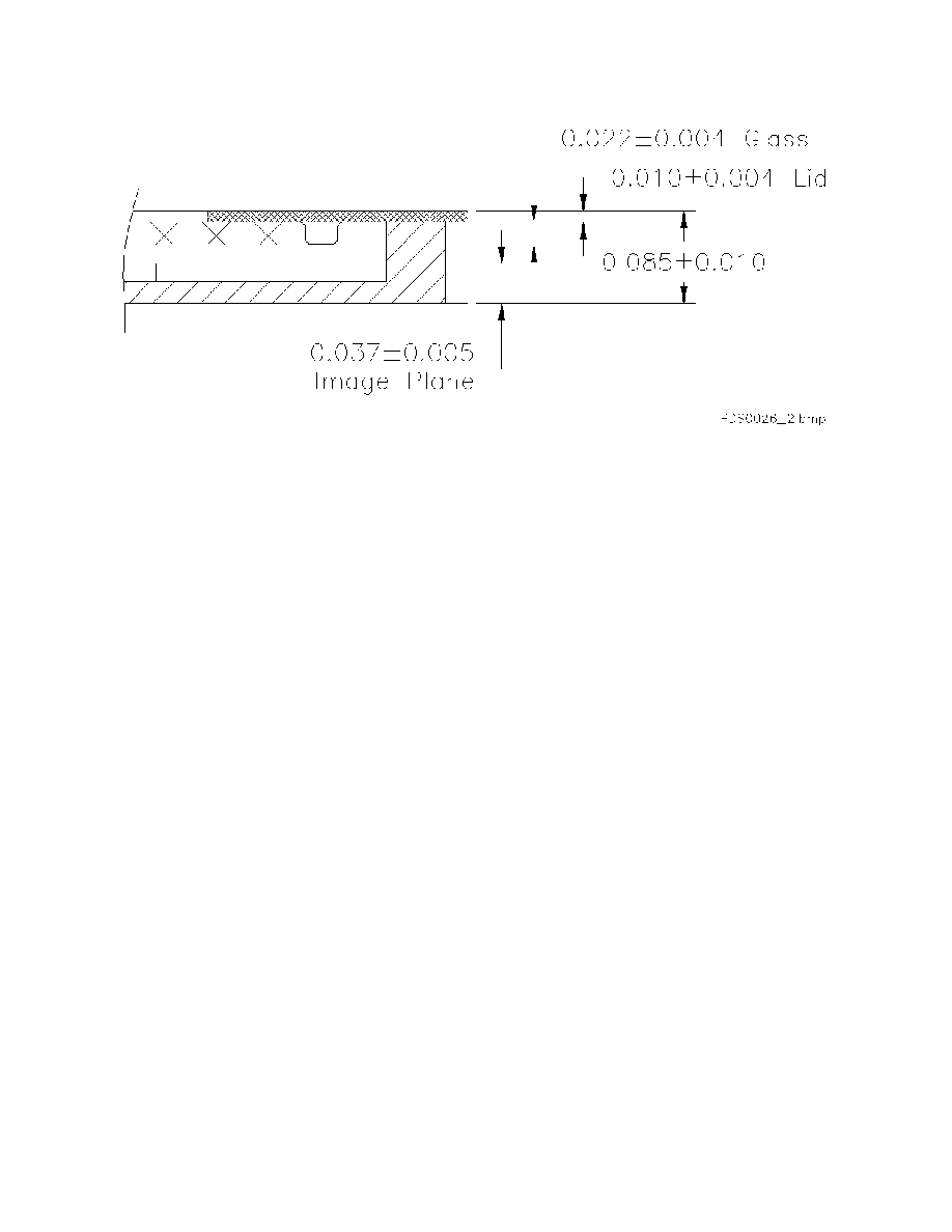
∞. The depth of the sensor's imaging surface is
shown in Figure 26. The responsivity of the imager to
red, blue and green is a function of the imager
quantum efficiency including the transmission of the
color filters (see Table 2 and Figure 3) and package
window transmission.
Package / Thermal Issues
The envelope drawing of the package is shown in
Figure 25. Without heatsinking the package, the die
temperature rise is 25-30
∞C above ambient. The lens
mount, which must be light-tight except for the lens
opening, will necessarily hold in imager-generated
heat. Thus, for any application for which the
operating temperature may go above room
temperature, we suggest that the PC board beneath
the imager be opened up to allow bonding an
aluminum or Kovar slug to the backside of the
package. There are numerous acceptable thermally
conductive epoxies available. The slug should cover
as much of the package area as possible and be
designed to accept a heatsink appropriate for the
intended operating temperature range.
ESD Precautions
The digital input pins, the digital output pins and the
power pins are protected against electro-static
discharge. However, the video outputs and the
PDBIAS pins are not ESD protected and appropriate
care in handling must be observed.
Ordering Information
Two models each having three quality grades are available. The structure of the complete part number is shown
below. The basic model number is common to all part numbers. There is a single package option at this time ≠
QuadHDTV
2003 ≠ Silicon Video, Inc. ≠ All rights reserved
PDS0026 Rev A Subject to change without notice. Page 21 of 26
designated as `LG' for the black alumina LCC package. Please see Figure 25 and Figure 26 for package details. The
color / monochrome selection is designated with a C or M respectively. Quality grades are described in table ? The
central region refers to a 1920H by 1080V rectangle concentric with the center of time image array. Bad pixels may
either be dead (dark) or hot (white). The `ES' designation applies to all parts at this time and indicates that parts are
not yet production qualified and therefore are not warranteed. Table 8 lists examples of valid part numbers and their
corresponding part descriptions.
QuadHDTV-8.3A-LG-C-G-ES
Model number
Quality grade (0 - 3)
Engineering
Structure of part number
pds0026_12.vsd
Package
Color/Mono (C or M)
Table 8. Example part numbers
Part Number
Description
QuadHDTV-8.3A-LG-C-0-ES
Color imager, highest quality grade
QuadHDTV-8.3A-LG-M-1-ES
Monochrome imager, quality grade 1
Table 9. Quality grade definitions
Quality Grade
Global
Central Region
Outside Central Region
0
No dead rows or columns
No cluster defects
Clusters: size & qty. TBD
Isolated bad pixels: qty TBD
1
No dead rows or columns
Clusters: size & qty. TBD
Isolated bad pixels: qty TBD
Clusters: size & qty. TBD
Isolated bad pixels: qty TBD
2
Isolated bad rows or columns
allowed (non-adjacent)
2 x 2 clusters: qty. TBD
Isolated bad pixels: qty. TBD
Clusters: size & qty. TBD
Isolated bad pixels: qty TBD
3
Multiple bad rows or columns
2 x 2 clusters: qty. TBD
Isolated bad pixels: qty. TBD
Clusters: size & qty. TBD
Isolated bad pixels: qty TBD
QuadHDTV
2003 ≠ Silicon Video, Inc. ≠ All rights reserved
PDS0026 Rev A Subject to change without notice. Page 22 of 26
Package Drawings
Figure 25. 64LCC Package Drawing including sensor position within package
QuadHDTV
2003 ≠ Silicon Video, Inc. ≠ All rights reserved
PDS0026 Rev A Subject to change without notice. Page 23 of 26
Figure 26. Package depth detail

QuadHDTV
2003 ≠ Silicon Video, Inc. ≠ All rights reserved
PDS0026 Rev A Subject to change without notice. Page 24 of 26
Characterization Criteria
Characterization measurements are guaranteed by
design and are not tested for production parts. Unless
otherwise specified, the measurements described
herein are characterization measurements.
Pixel Clock Frequency
The pixel clock frequency is the frequency at which
adjacent pixels can be reliably read. HDTV
compatibility requires that the pixel clock frequency
be 37.125 MHz for 30 frames/s operation although
the imager will operate at considerably higher pixel
rates. At higher pixel clock frequencies, the line
overhead time is proportionately reduced and this
eventually becomes the limiting factor in achieving
high quality video. The QuadHDTV
imager is
tested at a pixel clock frequency of 37.125 MHz.
Full Well
Full well (or Saturation Exposure) is the maximum
number of photon-generated and/or dark current-
generated electrons a pixel can hold. Full well is
based on the capacitance of the pixel at a given bias.
Full well is determined by measuring the capacitance
of all pixels for the operational bias. In reality, the
column circuitry will limit the signal swing on the
pixel, so full well is defined as the number of
electrons that will bring the output to the specified
saturation voltage.
Quantum Efficiency
Quantum Efficiency is a measurement of the pixel
ability to capture photon-generated charge as a
function of wavelength. This is measured at 10nm
increments over the wavelength range of the sensor
typically 300 to 1100 nm for monochrome or 380 to
780 nm for color. Measurements are taken using a
stable light source that is filtered using a
monochromator. The exiting light from the
monochromator is collimated to provide a uniform
flux that overfills a portion of the sensor area. The
flux at a given wavelength is measured using a
calibrated radiometer and then the device under test is
substituted and its response measured.
Linearity
Linearity is an equal corresponding output signal of
the sensor for a given amount of photons incident on
the pixel active area. Linearity is measured numerous
ways. The most straightforward method is plotting the
imager transfer function from dark to saturation and
fitting a `best fit' straight line from 1% to 75% of
saturation. The maximum peak-peak deviation of the
output voltage from the `best fit' straight line is
computed (E
pp
) over the fitting range. Linearity (L) is
then computed as shown below where V
FS
is the full-
scale voltage swing from dark to saturation measured
with sensor gain at 0.0 dB.
%
100
1
◊
-
=
FS
pp
V
E
L
Average Dark Offset
The `dark offset' is the voltage proportional to the
accumulated electrons for a given integration period,
that were not photon generated i.e. dark current.
There are a few sources in CMOS circuits for the
dark current and the dark current levels will vary even
for a given process. Dark offset is measured for a
33.3 millisecond integration time at T
A
= 25
∞C.
Read Noise
Read noise is the temporal or time variant noise in the
analog signal due to thermal noise in the analog path.
Read noise does not include spatial noise such as
fixed pattern noise (FPN) or photon shot noise. Read
noise is measured at the output of the imager with
proper loading and bandwidth limitations. Two
successive dark frames are captured and then
subtracted to remove spatial noise. Using this `noise'
frame, the standard deviation of a central region of
interest (ROI), typically 128 x 128, is measured and
scaled to compensate for the subtraction, giving a
measure of the sensor plus fixture noise. This
measurement is repeated with the imager replaced by
a low-noise d.c. source to determine the noise of the
test fixture alone. Noise sources add in quadrature,
thus the test setup noise is subtracted accordingly.
Image Lag
Image lag is the amount of residual signal in terms of
percent of full well on the current frame of video after
injecting the previous frame of video. Image lag is
measured by illuminating an ROI to 50% of
saturation for one frame and then rereading those
pixels for the next and subsequent frames without
light exposure. Any remaining residual signal will be
measured and recorded in terms of percent of full
well.

QuadHDTV
2003 ≠ Silicon Video, Inc. ≠ All rights reserved
PDS0026 Rev A Subject to change without notice. Page 25 of 26
Dynamic Range
Dynamic range is determined by dividing the full-
scale output voltage swing by the root mean squared
(rms) temporal read noise voltage and expressed as a
ratio or in decibels.
=
n
FS
e
V
DR
log
20
Modulation Transfer Function (MTF)
MTF is a measure of the imager's ability to sense and
reproduce contrast as a function of spatial frequency.
The Nyquist limit for the QuadHDTV sensor is 66
lp/mm. MTF is measured by illuminating a sensor
with a Davidson Optronics PR-10 squarewave burst
pattern having 11 discrete spatial frequencies.
Therefore, strictly speaking, we are measuring
Contrast Transfer Function (CTF) since squarewave
targets are easier to obtain and work with. Images are
captured with the input pattern oriented both
horizontally and vertically and saved as 8-bit images.
The sensor's response is derived from the captured
images as shown below where M is the measured
modulation and S
MAX
, S
MIN
are the digital numbers
(DN) associated with the spatial frequency under
evaluation.
MIN
MAX
MIN
MAX
S
S
S
S
M
+
-
input
output
M
M
CTF
MTF
Fixed Pattern Noise (FPN)
FPN, also known as dark signal nonuniformity
(DSNU), is a measure of pixel-to-pixel variation
when the array is in the dark. It is primarily due to
dark current differences, reset noise and synchronous
timing effects (at higher clock rates.) It is a signal-
independent noise and is additive to the other noise
powers. The FPN associated with the QuadHDTV
sensor consists of only column-column variations in
offset. Offset variations within any column are
inherently low due to the ACS technology. Similarly,
gain related FPN is almost non-existent due the ACS
technology. FPN is measured as a peak-to-peak
variation along a line of video averaged to remove
temporal noise. FPN in the QuadHDTV sensor is
measured per video output and represents an average
value among all eight of the video outputs.
Photoresponse Nonuniformity (PRNU)
PRNU is a measure of pixel-to-pixel variation in
output (responsivity) under uniform illumination
(usually illumination sufficient to bring the imager to
half-scale output at unity gain i.e. half-well.) PRNU is
a signal-dependent noise and is a multiplicative factor
of the photoelectron number. Using uniform
illumination, PRNU is measured over an ROI of
256H x 128V for each segment with a technique
designed to remove temporal noise. The standard
deviation of the histogram of all pixels in the ROI is
divided by the average value and multiplied by 100%.
%
100
◊
=
AVG
RMS
V
V
PRNU

QuadHDTV
2003 ≠ Silicon Video, Inc. ≠ All rights reserved
PDS0026 Rev A Subject to change without notice. Page 26 of 26
References
1. Terry
Zarnowski,
"The Active Column Sensor CMOS Imager ≠ Giving Better Images for Less," April
2000, Sensors, Advanstar Communications.
2. T.L.Vogelsong, J.J.Zarnowski, M.Pace and T.Zarnowski, "Scientific/industrial camera-on-a-chip using
Active Column Sensor CMOS imager core," SPIE Vol. 3965-11, Jan 2000.
3. J. Zarnowski, M. Pace and M. Joyner, "1.5 FET per Pixel Standard CMOS Active Column Sensor,"
SPIE Vol. 3649-27, Jan 1999.
4. R.M. Iodice, J.J. Zarnowski, M.A. Pace, M. Joyner, T.L. Vogelsong, T.L. Zarnowski, "Ultra-high speed
CMOS scanning linear imager family," SPIE Vol. 4306-12, Jan 2001.
5. R.M. Iodice, C. Hong, M. Joyner, D. Paker, "Broadcast quality 3840 x 2160 color imager operating at
30 frames/s," SPIE Vol. 5017-01, Jan 2003.
NOTICE
Silicon Video, Inc. (SVI) reserves the right to make product modifications or discontinue products or services
without notice. Customers are advised to obtain latest written specifications or other relevant information prior to
ordering product or services. Information provided by Silicon Video, Inc. is believed to be accurate at time of
publication release. SVI shall not be held liable for any damages, consequential or inconsequential resulting from
errors or omissions of documentation, or use of our products.
Product sales are subject to the SVI Terms and Conditions of Sale in force at the time of order acknowledgement.
SVI assumes no liability for customer products or designs. SVI does not warrant or represent that any license, either
expressed or implied, is granted under any patent, copyright, or any other intellectual property right of SVI for any
product or process for which SVI products or services are used. SVI does not endorse, warrant, or approve any third
party's products or service information that may be published by SVI.
SVI's products are not designed, authorized, or warranted for use in life support devices or systems, or any other
critical application that may involve death, injury, property or environmental damages. Using SVI's products for any
critical application is fully at the risk of the customer and their end users and assigns.
This imager may be covered under the following patent: 6,084,229