 | –≠–ª–µ–∫—Ç—Ä–æ–Ω–Ω—ã–π –∫–æ–º–ø–æ–Ω–µ–Ω—Ç: RAD750 | –°–∫–∞—á–∞—Ç—å:  PDF PDF  ZIP ZIP |
RAD750
TM
TM
Board
Hardware User's Manual
Document Number
234A533
Release Date
December 20, 2000
Copyright by BAE SYSTEMS
All Rights Reserved

i
Document #: 234A533
RAD750 3U CompactPCI
Hardware Users Manual
Notices
Before using this information and the product it supports, be sure to read the general information on the
back cover of this book.
Trademarks
The following are trademarks of International Business Machines Corporation in the United States, or
other countries, or both:
IBM
IBM Logo
PowerPC
PowerPC 750
The following are trademarks of BAE SYSTEMS in the United States, or other countries, or both:
RAD750
The following are registered trademarks of PCI Industrial Computer Manufacturing Group in the United
States, or other countries, or both:
PICMG
CompactPCI
Other company, product, and service names may be trademarks or service marks of others.
Preliminary Edition (Version 2.10, 12/21/2000)
This unpublished document is the RAD750
TM
Board Hardware Users Manual. Make sure you are using
the correct edition for the level of the product.
This document contains information on a new product under development by BAE SYSTEMS. BAE
SYSTEMS reserves the right to change or discontinue this product without notice.
© BAE SYSTEMS 2001.
All rights reserved.

ii
Document #: 234A533
RAD750 3U CompactPCI
Hardware Users Manual
Preface
Notice for reviewers:
This is an update to the preliminary release of this document.
At this time, some of the information contained in this document is in a state of flux until completion of first
Flight unit bring-up, and may be slightly behind the hardware specifications.
Items marked
TBA
or
TBD
will be filled in for a subsequent release.
When reviewing the document, please keep the following in mind when providing comments:
∑
Is the document presented in a usable order?
∑
Do I need to include any test set information?
∑
Since this is intended to be an all-encompassing, standalone document, is there any information
that can be found somewhere else that should be included here
∑
Does the document provide enough information to stand-alone?
∑
Has too much detail been provided in some areas? What document should that detail be placed?
∑
What information is missing and should be added?
∑
Does the appendix belong as a separate document or should it be merged into this document?

iii
Document #: 234A533
RAD750 3U CompactPCI
Hardware Users Manual
Table of Contents
1
USING THIS MANUAL ....................................................................................................................1
1.1
A
UDIENCE OF THE
H
ARDWARE
U
SERS
M
ANUAL
..............................................................................1
1.2
O
VERVIEW OF THE
M
ANUAL
S
ET
...................................................................................................1
1.3
S
OFTWARE
U
SERS
M
ANUAL
.........................................................................................................2
1.4
RAD750 / P
OWER
PCI S
ET OF
D
ATA
S
HEETS
...............................................................................2
1.5
R
EVISION
H
ISTORY
.....................................................................................................................2
1.6
C
ONVENTIONS
/ N
OMENCLATURE
.................................................................................................2
1.7
T
ERMINOLOGY
............................................................................................................................3
2
OVERVIEW......................................................................................................................................5
2.1
RAD750 3U C
OMPACT
PCI B
OARD
F
UNCTIONS
............................................................................5
2.1.1
RAD750 PowerPC Processor................................................................................................6
2.1.2
Power PCI Bridge Function ...................................................................................................6
2.1.3
SUROM ................................................................................................................................7
2.1.4
Local Memory .......................................................................................................................7
2.1.5
Clocking................................................................................................................................7
2.1.6
Power Regulation and Consumption .....................................................................................8
2.2
S
PECIFICATION
...........................................................................................................................8
2.3
O
RDERING
I
NFORMATION
.............................................................................................................9
2.4
SUROM D
ESCRIPTION
.............................................................................................................10
3
INSTALLATION INSTRUCTIONS..................................................................................................11
3.1
S
AFETY
P
RECAUTIONS
..............................................................................................................11
3.2
U
NPACKING AND
I
NSPECTING
.....................................................................................................11
3.2.1
Unpacking...........................................................................................................................11
3.2.2
Board Identification .............................................................................................................11
3.2.3
Malfunction or damage to the board or connected components ...........................................11
3.3
W
ARNINGS
...............................................................................................................................12
3.4
C
OMPACT
PCI C
ONNECTOR
K
EYING
............................................................................................12
3.5
I
NSERTION
L
EVERS
/ J
ACK
S
CREWS
............................................................................................12
3.6
W
EDGELOCKS
..........................................................................................................................12
3.7
P
OWER
R
EQUIREMENTS
............................................................................................................12
3.8
B
ACKPLANE
D
ESIGN
G
UIDELINES
................................................................................................12
3.9
P
OWER
-
UP AND
O
PERATIONAL
D
ESCRIPTION
...............................................................................13
3.9.1
Power-up ............................................................................................................................13
3.9.2
Operation Description .........................................................................................................13
3.9.3
Resetting the RAD750 board...............................................................................................13
3.10
T
ROUBLESHOOTING
..................................................................................................................15
3.10.2
Debugging.......................................................................................................................16
3.11
RAD750 B
OARD
E
LECTRICAL
C
ONNECTORS
...............................................................................17
3.11.1
J1 Connector Pin Assignment .........................................................................................17
3.11.2
J2 Connector Pin Assignments........................................................................................18
3.12
C
OMPACT
PCI S
LOT
G
UIDELINES FOR
M
ULTIPROCESSOR
C
ONFIGURATIONS
...................................19
3.13
C
OMPATIBILITY WITH
RAD6000 .................................................................................................20

iv
Document #: 234A533
RAD750 3U CompactPCI
Hardware Users Manual
3.14
F
RONT
P
ANEL
C
ONNECTOR
.......................................................................................................20
3.14.1
J7 Pin Assignments.........................................................................................................20
4
HARDWARE / ELECTRICAL.........................................................................................................21
4.1
RAD750..................................................................................................................................21
4.1.1
RAD750 Microprocessor Features ......................................................................................23
4.2
P
OWER
PCI .............................................................................................................................25
4.2.1
Environment........................................................................................................................26
4.2.2
Compliance Summary.........................................................................................................26
4.2.3
Architecture Overview .........................................................................................................26
4.2.4
Power PCI Features............................................................................................................27
4.2.5
Endian Conventions ............................................................................................................40
4.2.6
RAD750 Interrupts and Vector Interrupts.............................................................................42
5
EXTERNAL ELECTRICAL INTERFACE........................................................................................50
5.1
C
OMPACT
PCI D
EFINED
S
IGNALS
................................................................................................50
5.1.1
PCI Interface I/O .................................................................................................................56
5.1.2
PCI Central Resource I/O (external) ....................................................................................60
5.1.3
PCI Miscellaneous Interface................................................................................................61
5.2
N
ON
-PCI I
NTERFACES
..............................................................................................................61
5.2.1
JTAG Interfaces..................................................................................................................66
5.2.2
UART Interface ...................................................................................................................71
5.2.3
Interrupts and Discretes ......................................................................................................72
5.2.4
Resets and Clocks ..............................................................................................................75
5.2.5
Configuration Inputs ............................................................................................................75
5.3
P
OWER
I
NTERFACES
.................................................................................................................76
6
HARDWARE / MECHANICAL .......................................................................................................77
6.1
L
OCATION
O
VERVIEW
................................................................................................................78
6.2
G
ROUNDING
.............................................................................................................................79
6.2.1
Structural Grounding ...........................................................................................................79
6.2.2
Circuit Grounding, General..................................................................................................79
6.2.3
Wire Shield Grounding ........................................................................................................79
6.2.4
ESD Grounding...................................................................................................................79
7
MANUFACTURING .......................................................................................................................81
7.1
O
RGANIC
M
ATERIALS
................................................................................................................81
7.2
I
NORGANIC
M
ATERIALS
..............................................................................................................83
7.3
P
ROCESSES
.............................................................................................................................83
7.4
B
ILL OF
M
ATERIALS
...................................................................................................................85
8
DOCUMENTATION .......................................................................................................................88
8.1
S
UGGESTED
R
EADING
...............................................................................................................88
8.1.1
General PowerPC Information.............................................................................................88
8.1.2
IBM PowerPC Documentation.............................................................................................88
8.2
A
PPLICABLE
D
OCUMENTS
..........................................................................................................89
8.2.1
Specifications......................................................................................................................89
8.2.2
Standards ...........................................................................................................................90

v
Document #: 234A533
RAD750 3U CompactPCI
Hardware Users Manual
8.2.3
Design Descriptions and Design Guides..............................................................................90
9
COMMENTS ..................................................................................................................................91

vi
Document #: 234A533
RAD750 3U CompactPCI
Hardware Users Manual
List of Figures
Figure 1: Notional C&DH Architecture using a RAD750 board ..................................................................5
Figure 2: RAD750 Board Block Diagram ..................................................................................................6
Figure 3: Board identification label .........................................................................................................11
Figure 4: RAD750 Microprocessor Block Diagram..................................................................................22
Figure 5: Power PCI Chip on a Processor Board ....................................................................................26
Figure 6: Power PCI Cores ....................................................................................................................27
Figure 7: PCI Core Block Diagram .........................................................................................................28
Figure 8: 60X Core functional block diagram ..........................................................................................32
Figure 9: GP Timer Functional Block Diagram........................................................................................35
Figure 10: Clock Generation Logic .........................................................................................................36
Figure 11: Data Transfers in Big Endian Mode. ......................................................................................41
Figure 12: Data Transfers in Little Endian Mode.....................................................................................42
Figure 13: Power PCI Interrupt Collection ..............................................................................................43
Figure 14: Power PCI INT_L Interrupt Tree ............................................................................................44
Figure 15: Power PCI MCP Generation Tree..........................................................................................46
Figure 16: Power PCI Checkstop Generation Tree and Vector Interrupt Tree .........................................49
Figure 17: JTAG Backpanel Interface I/O ...............................................................................................67
Figure 18: JTAG RAD750 Interface I/O ..................................................................................................69
Figure 19: JTAG Slave Interface I/O.......................................................................................................70
Figure 20: Peripheral Device Interface I/O..............................................................................................71
Figure 21: Isometric View of the RAD750 Board Layout .........................................................................77
Figure 22: Standard View of the RAD750 Board Layout .........................................................................78
Figure 23: RAD750 Board Layout ..........................................................................................................79

vii
Document #: 234A533
RAD750 3U CompactPCI
Hardware Users Manual
List of Tables
Table 1 - RAD750 3U CompactPCI board Maximum Power Consumption with V
cc
= 3.3
±
5% VDC, GND =
0 VDC, -55
T
j
< 125
o
C....................................................................................................................8
Table 2 - RAD750 3U CompactPCI board Typical Power Consumption with V
cc
= 3.3 VDC, GND = 0 VDC,
T
MR
= 25
o
C........................................................................................................................................8
Table 3 - Specification of the RAD750 board (Flight Configuration) ..........................................................8
Table 4 - RAD750 board Part Number Listing ........................................................................................10
Table 5 - CompactPCI J1 Connector Signals .........................................................................................17
Table 6 - CompactPCI J2 Connector Pinouts .........................................................................................18
Table 7 - Front Panel Connector J7 Pin Assignments.............................................................................20
Table 8 - PCI User Defined Register Definitions .....................................................................................28
Table 9 - UART Baud Rate Programming ..............................................................................................34
Table 10 - Power PCI Power Management Operational Modes ..............................................................40
Table 11 - Interrupt Register Definition...................................................................................................45
Table 12 - Error Mechanisms .................................................................................................................46
Table 13 - RAD750 board Interrupt Latencies.........................................................................................49
Table 14 - X2000 System Flight Computer PCI Interface Signals ...........................................................50
Table 15 - X2000 System Flight Computer Non-PCI Signals ..................................................................62
Table 16 - PID Definition Table ..............................................................................................................73
Table 17 - Organic Materials ..................................................................................................................82
Table 18 - Inorganic Materials................................................................................................................83
Table 19 - Processes .............................................................................................................................83
Table 20 - Bill of Materials......................................................................................................................85

1
Document #: 234A533
RAD750 3U CompactPCI
Hardware Users Manual
1 Using This Manual
This section does not provide information on the product, but on features of the manual itself:
∑
its structure,
∑
special layout conventions, and
∑
related documents.
This manual is separated into two parts: The main Hardware User's Manual (this document), and an
Appendix. The Appendix contains the detailed register maps and descriptions that are part of the Power
PCI ASIC and how they are utilized on this board.
1.1 Audience of the Hardware Users Manual
The Hardware Users Manual is intended for hardware and software developers installing and integrating
the RAD750 3U CompactPCI board into their systems. Software engineers who are developing or
troubleshooting code are expected to use the interface portion of this manual. The manual includes full
descriptions of all dedicated I/O locations, specific I/O commands and registers, programmed I/O, and I/O
command partitioning. It includes a detailed memory map with the paging scheme.
1.2 Overview of the Manual Set
The Hardware Users Manual provides a comprehensive hardware guide to your board.
IMPORTANT: Take a moment to examine the "Table of Contents" of the Hardware Users Manual to see
how this documentation is structured. This will be of value to you when looking for information in the
future. The Hardware Users Manual includes:
∑
A brief overview of the product, the specifications, and the ordering information: see Section 2
"Overview".
∑
The installation instructions for powering up the board: see Section 3 "Installation Instructions". It
includes the default configuration, initialization, and connector pinouts.
∑
A detailed hardware description: See Section 4"Hardware / Electrical".
∑
A detailed description of the CompactPCI connector I/O: see Section 5 "CompactPCI Defined
Signals".
∑
A detailed mechanical description of the RAD750 board: see Section 6 "Hardware / Mechanical".
∑
A description of the RAD750 board manufacturing processes: see Section 7 "Manufacturing".
∑
Sources of additional information, including the latest version of the document: see Section 8
"Documentation".
This manual includes a pictorial/diagrammatic description of the RAD750 board hardware internal
functions. External interfaces are included to ensure logical written and pictorial continuity and
completeness. The descriptions are written so that reference to other documents is not required for
immediate understanding. The manual includes explanations of internal hardware. The Power PCI
internal controller, it's addressing modes, I/O control and memory mapping are explained in detail.
Interrupts, status registers, fault types, causes and protection are included. Error detection and correction
strategies, as used, are detailed. The test, power, electronic and electrical interface specifics are
described. Mechanical, structural and environmental requirements and interfaces are also detailed. A
troubleshooting tree is included.
All implemented I/O commands are included. This manual includes detailed coverage and explanation of
interrupts, and memory mapping. Peculiar system interfaces such as dedicated memory locations,
channel register definitions, command code assignments and definitions, multiple channel priorities, and
page register access are detailed. Although this manual is a software tool, hardware handling of the I/O
process internal and external to the hardware/software is included. All hardware/software configurations
are included. Interfaces peculiar to the test configuration are clearly described and illustrated.
2
Document #: 234A533
RAD750 3U CompactPCI
Hardware Users Manual
The Hardware Users Manual addresses the engineering model and flight versions of the RAD750 board
in detail.
1.3 Software Users Manual
In addition to the Hardware Users Manual, BAE SYSTEMS provides a software Users Manual and a
Support Equipment Users Manual. These two documents describe how to develop software for the
RAD750 3U CompactPCI board, describe the Board Support Package (BSP) and SUROM products, and
the recommended test development environment for the RAD750 board. See Section 8 to see how to
obtain copies of these 2 documents.
1.4 RAD750 / Power PCI Set of Data Sheets
The RAD750 / Power PCI Set of Data Sheets, which contains the data sheets relevant for configuring and
integrating the board into systems, is packaged in an separate binder to ease handling. It is always
shipped together with the Hardware Users Manual. The RAD750 / Power PCI Set of Data Sheets
includes the following datasheets:
∑
LM/STC RAD750
∑
LM/STC PowerPC-to-PCI Bridge
∑
Q-Tech Oscillator
∑
LM/STC 256 Mbit SDRAM Stack
∑
SEI EEPROM
∑
OmniRel Voltage DC/DC Converter
1.5 Revision History
REVISION
REVISION HISTORY
DATE
1.0
Initial release
9/9/99
2.0
Updated Release ≠ Environmental Spec changes, minor updates
4/28/00
3.1
12/20/00
1.6 Conventions / Nomenclature
The following conventions are used in the text of this document:
The following conventions apply except were specifically noted.
∑
In PowerPC terminology, multiple bit fields are numbered from 0 to n, where 0 is the MSB and n
is the LSB.
∑
PCI terminology follows the convention that bit 0 is the LSB and n is the MSB.
∑
When counting N elements, the first element is designated element 0 and the last element is
designated element N-1.
∑
Information of particular importance is in bold typeface and is further highlighted by the NOTE
reference.
∑
Signal names are fully capitalized and use a bold font: SIGNAL1
∑
Active low PCI I/O signals are suffixed with the `#' symbol to be consistent with the PCI
specification. All other active low signals are suffixed with `_L'. Note that this does not
supersede the coding requirement that all active low signal names are coded using the `_L' suffix:
FRAME#, SIGNAL2_L
∑
Internal register names have leading caps and use a bold font: Device ID, Status
∑
Register field or bit names have leading caps and use a bold and italicized font: Bus Master
∑
All numbers are expressed in decimal, except addresses and memory or register data, which are
expressed in hexadecimal: 0x'0F'; or binary: 0b'0110' or `1', following the 'C' programming
language convention.

3
Document #: 234A533
RAD750 3U CompactPCI
Hardware Users Manual
∑
An `n' denotes bit definitions.
∑
An `xnnnn' denotes word definitions.
∑
The multipliers 'k', 'M' and 'G' have their conventional scientific and engineering meanings of *10
3
,
*10
6
and *10
9
, respectively. The only exception to this is in the description of the size of memory
areas, when 'K', 'M' and 'G' mean *2
10
, *2
20
and *2
30
, respectively.
∑
When describing transfer rates, `k', `M' and `G' mean *10
3
, *10
6
and *10
9,
not *2
10
, *2
20
and *2
30
,
respectively.
∑
Names of external signals which have a single destination are of the form <source
block>_<destination block>_<signal>.
∑
Names of external signals which have a multiple destinations are of the form <source
block>_<signal>.
1.7 Terminology
The following terms are used throughout this document.
Term
Description
Active Bank
A physical bank (or sub-bank) of SDRAM which has already received a "Bank
Activate" command, thereby selecting a row. Once a bank is active, the bank
must be precharged before another "Bank Activate" command can be issued to
select a different row.
Active Scrubbing
A memory scrubbing process in which the memory controller inserts extra
memory read operations during idle cycles to detect and correct data errors.
ASIC
Application Specific Integrated Circuit
Bank
A memory part (or, more typically, a group of memory parts) which provides a
complete data vector. A complete data vector typically contains 64-bits of data
and 8, 16 or 24 ECC bits.
Bank Miss
A memory operation that does not address an open bank.
BAR
Base Address register
Big Endian
The ordering of data such that the most significant byte is stored at the lowest
order address.
BIST
Built-in Self Test
Byte
An 8-bit value.
Byte-Enabled Write
A write in which some bytes of a data beat are not stored to memory.
Cache Line
A cache line consists of 4 double words (32 bytes).
Character
In this document a character refers to a byte of data that is stored into a FIFO.
Column
In the context of internal SDRAM layout, the column is used in conjunction with
the SDRAM row to select a single bit (per data output bit) from the SDRAM
memory matrix.
Data Beat
A single unit of data, usually a data beat is a double word.
Double word
A 64-bit value.
Doze Mode
A power management mode that consumes more power than Sleep Mode, but
less power than Normal Mode. . See also Nap, Normal and Sleep Modes.
DWORD
32-bit block of data (4 bytes)
FIFO
First In First Out. Bank of registers that store data, such that the first set of data
stored is the first data that is read out.
Half word
A 16-bit value.
HDL
Hardware Description Language - A language for describing digital electronic
systems.
JTAG
Joint Test Action Group Interface. Refers to the test interface standardized in
IEEE 1149.1a
JTAG Master
A TAP Controller and associated logic that controls JTAG Slave(s) located
outside the function.
Little Endian
The ordering of data such that the most significant byte is stored at the highest

4
Document #: 234A533
RAD750 3U CompactPCI
Hardware Users Manual
Term
Description
order address. The endian ordering of data never extends beyond an 8 byte
group of storage.
lsb
least-significant bit
LSB
Least-Significant Byte
Marking State
Logic `1'.
Memory Scrubbing
The process of writing memory to correct a data error in the memory.
Memory Sparing
The process of using extra (or spare) columns of memory to replace failed
columns.
msb
Most-significant bit
MSB
Most-Significant Byte
Munging
A transformation of the address to convert between endian modes.
Nap Mode
A power management mode of the RAD750 or Power PCI, which consumes
more power than Sleep Mode, but less power than Normal Mode. See also
Normal, Doze and Sleep Modes.
Normal Mode
The typical (full-power) operational mode of the RAD750 or Power PCI. See
also Doze, Nap and Sleep Modes.
One-hot State
Machine
Each state of the state machine has its own register bit.
Open Bank
Same as Active Bank.
Parity
Can be odd or even. Even Parity indicates that the number of ones in the data
and parity bit is even, and likewise odd parity indicates that the number of ones
is odd.
Passive Scrubbing
A memory scrubbing process in which the Power PCI memory controller only
looks for and corrects data errors at memory locations that the Power PCI has
read.
PCI
Peripheral Component Interconnect. Refers to the PCI Local Bus as defined in
the PCI Local Bus Specification. Version 1.0 of the PCI specification was
developed by Intel Corporation and released on 6/22/92. The PCI Special
Interest Group (SIG) currently manages the specification.
POR
Power on Reset
Precharge
An SDRAM command that closes an open bank.
Record
A VHDL construct that can contain many signals of different types.
Row
In the context of internal SDRAM layout, a single bit-line selected by the Bank
Activate command. When used in conjunction with an SDRAM column, a single
bit (per data output bit) is selected from an SDRAM memory matrix.
RTL
Register Transfer Level. Refers to a HDL coding style that is characterized by
the explicit definition of all register to register transfers within the device being
described.
Sleep Mode
The lowest power operational mode of the RAD750 or Power PCI. See also
Normal, Doze and Nap Modes.
Spacing State
Logic `0'.
Sub-bank
A single internal bank in an SDRAM part with multiple internal banks.
VHDL
VHSIC Hardware Description Language - standardized in IEEE standard 1076
VHSIC
Very High Speed Integrated Circuit
Word
A 32-bit value.
5
Document #: 234A533
RAD750 3U CompactPCI
Hardware Users Manual
2 Overview
The RAD750 3U CompactPCI board is designed to provide the main computational capability for a
spacecraft. Figure 1 shows the RAD750 3U CompactPCI board combined with other I/O and memory
boards to form the main processing elements of an spacecraft avionics command and data handling
(C&DH) system.
Bulk Memory
Bulk Memory
Spacecraft
I/O and TT&C
Spacecraft
I/O and TT&C
RAD750
RAD750
Payload I/O
Payload I/O
PCI and JTAG Buses
Figure 1: Notional C&DH Architecture using a RAD750 board
2.1 RAD750 3U CompactPCI Board Functions
As shown in Figure 2, the RAD750 board consists of the following major functions:
∑
RAD750 PowerPC processor and its 3.3V/2.5V regulator,
∑
Power PCI Bridge function and its oscillator,
∑
SUROM, and
∑
Local Memory.
The following section is divided into subsections corresponding to the top-level capabilities of each of
these major functions.
6
Document #: 234A533
RAD750 3U CompactPCI
Hardware Users Manual
RAD750 CPU
Power PCI Bridge
Local Memory
SUROM
OSC
Memory Control
Memory Data
6xx
Data
6xx
Address
& Control
Clocks,
Interrupts
and
Controls
Memory Address
PCI Bus
UART Port
Slave
JTAG Port
RAD750
JTAG Port
Master
JTAG Port
Reset,Interrupts
& Discretes
Clock
2.5V
Regulator
3.3V
2.5V
Configuration
Figure 2: RAD750 Board Block Diagram
2.1.1 RAD750 PowerPC Processor
The RAD750 is functionally and pin-for-pin compatible with a commercial PowerPC 750. The RAD750
PowerPC processor provides the RAD750 board with the following functions:
∑
PowerPC 750 Instruction Set Architecture (ISA),
∑
Floating Point Unit which implements the IEEE-754 floating point standard
∑
32 Kbytes of instruction cache,
∑
32 Kbytes of data cache, and
∑
An L2 cache interface (No L2 cache is implemented on the RAD750 board).
A more detailed description can be found in Section 4.1.1.
2.1.2 Power PCI Bridge Function
The primary function of the Power PCI Bridge is to provide a bridge between the native RAD750 6xx bus
and a Version 2.1 compatible PCI bus. The Power PCI Bridge provides the RAD750 board a:
∑
Version 2.1 compatible PCI bus interface,
∑
PCI burst mode with contiguous data transfers,
∑
PCI arbitration and resource control,
∑
Memory data and address interface,
∑
Memory error detection and correction (EDAC),
∑
Auto memory scrub,
∑
Cache snooping on system memory accesses,
∑
16550 compatible UART interface,
∑
RAD750, PCI and JTAG clock control,
∑
Three programmable timers which may be used to provide operating system tick and cycle start
interrupts,

7
Document #: 234A533
RAD750 3U CompactPCI
Hardware Users Manual
∑
A watchdog timer,
∑
Interrupts and discretes,
∑
Embedded micro-controller that may control complex DMA operations,
∑
Power saving modes to match the RAD750,
∑
Dual JTAG master interfaces, and a
∑
JTAG tap controller.
The Power PCI provides enhanced features over the most used COTS PowerPC bridge chip (Motorola
MPC-106), and thus it is not pin compatible with any COTS bridge chip. More details on the Power PCI
chip can be found in Section 4.2. In addition, the many registers of the Power PCI chip are discussed in
more detail in the Appendix to this User's Manual.
2.1.3 SUROM
The SUROM consists of 256 Kbytes of nonvolatile EEPROM memory and provides nonvolatile program
store for the initial program load of the RAD750. The SUROM is organized as 128K x 24 with 16 bits of
data and 8 bits of error correction code. All SUROM memory can be directly addressed by the RAD750
and by any internal master function of the Power PCI. This includes the internal EMC, an external JTAG
master connected through the backpanel or Power PCI JTAG port to the RAD750 board, or any PCI
initiator device connected to the RAD750 board. The error correction code provides single bit error
correction and double bit error detection. Section 2.4 provides a brief description of the contents of
SUROM. A more detailed description can be found in the software Users Manual (see Section 8 for
directions on obtaining the manual).
2.1.4 Local Memory
The Local Memory consists of 128 Mbytes of Synchronous DRAM (SDRAM) and provides processor
program and data store. All local memory is directly addressable by the RAD750 and by any internal
master function of the Power PCI. The local memory is organized as 16M x 80 with 64 bits of data and
16 bits of error correction code. The error correction coding provides single nibble error correction and
double nibble error detection so that cluster SEU events within the SDRAM components will be
correctable. The Local Memory, when placed in a self-refresh mode by software, retains its contents
during a reset of any duration so long as the RAD750 3U CompactPCI board power input is not
interrupted, however, scrubbing of the memory is disabled during self-refresh so SEU errors will be
accumulating.
2.1.5 Clocking
The RAD750 board uses a single 33 MHz Oscillator to drive the PCI Clock, Processor Clock and Real
Time Clock inputs on the Power PCI chip. Section 4.2.4.7 provides more details on the clock generation
logic, which is contained in the Power PCI chip. Details of the configuration and status registers used to
control the clock function can be found in the Appendix to this User's Manual. The RAD750 board is
configurable to use the 33 MHz Oscillator to run the RAD750 at the following speeds:
∑
133 MHz using a 4x Tap (Full speed mode)
∑
99 MHz using a 3x Tap
∑
66 MHz using a 2x Tap
∑
33 MHz using no PLL
∑
16.5 MHz using no PLL and a divide by 2 (half speed mode)
∑
8.25 MHz using no PLL and a divide by 4 (quarter speed mode), and
∑
4.125 MHz using no PLL and a divide by 8 (eighth speed mode).
Clock speeds higher than 133 MHz will be available at a future date.
8
Document #: 234A533
RAD750 3U CompactPCI
Hardware Users Manual
The RAD750 board is configurable to use the 33 MHz Oscillator to run the PCI Bus at the following
speeds:
∑
33 MHz
∑
16.5 MHz
∑
8.25 MHz
∑
4.125 MHz
The RAD750 board uses the 33 MHz Oscillator to run the real time clock at 33 MHz divided down by 4, 8,
16, or 32.
2.1.6 Power Regulation and Consumption
The RAD750 board draws all required power from an external 3.3V supply. The power source is
expected to be regulated to 3.3V
±
5% and a maximum ripple of 60 mV p-p with a power converter
switching frequency of 1 MHz. An on-card regulator provides the +2.5V required for the RAD750. The
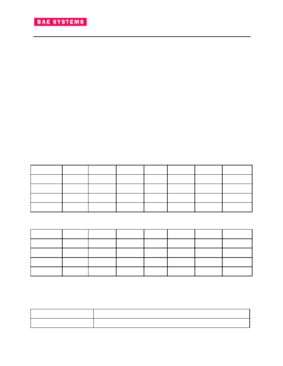
RAD750 board has the power consumption characteristics listed in Table 1 and Table 2. Maximum
power includes worst case temperature, voltage, and post-radiation exposure. Typical power is an
average value measured at V
cc
= 3.3V and +25
∞
C in a system executing typical applications or
benchmarks.
Table 1 - RAD750 3U CompactPCI board Maximum Power Consumption with V
cc
= 3.3
±
5% VDC,
GND = 0 VDC, -55
T
j
< 125
o
C
Mode
132 MHz
99 MHz
66 MHz
33 MHz
16.5 MHz
8.25 MHz
4.125 MHz
Full-On (W)
14.5 W
11.5 W
10.0 W
8.5 W
7.1 W
6.3 W
6.0 W
Doze (W)
5.2 W
4.6 W
4.0 W
3.4 W
3.1 W
2.9 W
2.9 W
Nap (W)
2.7 W
2.7 W
2.7 W
2.7 W
2.7 W
2.7 W
2.7 W
Sleep (W)
2.3 W
2.3 W
2.3 W
2.3 W
2.3 W
2.3 W
2.3 W
Table 2 - RAD750 3U CompactPCI board Typical Power Consumption with V
cc
= 3.3 VDC, GND = 0
VDC, T
MR
= 25
o
C
Mode
132 MHz
99 MHz
66 MHz
33 MHz
16.5 MHz
8.25 MHz
4.125 MHz
Full-On (W)
10.0 W
8.0 W
7.0 W
5.9 W
4.9 W
4.4 W
4.2 W
Doze (W)
4.3 W
3.8 W
3.3 W
2.8 W
2.6 W
2.4 W
2.4 W
Nap (W)
2.2 W
2.2 W
2.2 W
2.2 W
2.2 W
2.2 W
2.2 W
Sleep (W)
1.9 W
1.9 W
1.9W
1.9 W
1.9 W
1.9 W
1.9 W
2.2 Specification
Table 3 provides a high level specification of the RAD750 board Flight Unit.
Table 3 - Specification of the RAD750 board (Flight Configuration)
Item
Description
Processor
RAD750

9
Document #: 234A533
RAD750 3U CompactPCI
Hardware Users Manual
Item
Description
Shared main memory
128-MByte SDRAM with ECC
Board
Conduction Cooled, double sided, CompactPCI RAD750 3U format
CompactPCI interface
PowerPC-to-PCI bridge, 32 bit, 33 MHz, full system slot function or
peripheral slot.
Serial I/O
JTAG and UART I/O on front panel and CompactPCI J2 connector
(factory option)
Counters/timers
Three 32-bit, programmable, and a Watchdog Timer
SUROM
256 KByte On-board programmable, Hardware write protection
Additional features
26 Programmable discrete and Interrupts on CompactPCI J2 connector,
PCI Ready Parity on CompactPCI J1 connector
Power consumption
see Section 2.1.6 "Power Regulation and Consumption"
Environmental Conditions:
Temperature (operating)
Temperature (storage)
Humidity
Thermal Shock
Vibration
-55 ∞C to +70 ∞C
-55 ∞C to +125 ∞C
5 % to 95 % non-condensing
±
5
∞
C per minute
20 to 2000 Hz @ 12.3grms
Radiation
TBD
SEU
100 KRad Total dose
Performance:
RAD750
PCI Bus
- DMA Read(*)
- DMA Write(*)
240 Dhrystone 2.1 MIPS, 5.75 SPECint95 and 3.25 SPECfp95 @ 133
MHz
90 Mbytes per second
130 Mbytes per second
Standards compliance
PCI Local Bus Specification Rev. 2.1 CompactPCI Specification Rev.
D1.10
(*) ≠ External DMA controller with no snooping HITS during transfer
2.3 Ordering Information
This section provides the part numbering nomenclature for the RAD750 boards. Note that the individual
part numbers correspond to combinations of processor core frequencies, populated memory, and
environmental levels. For availability of RAD750 board variations, contact BAE SYSTEMS in Manassas,
Virginia or visit our web site at
www.rad750.com
. Table 4 shows the designated part numbers that are
currently offered.

10
Document #: 234A533
RAD750 3U CompactPCI
Hardware Users Manual
Table 4 - RAD750 board Part Number Listing
Part Number /
Designation
Maximum
Processor
Frequency
SUROM
SDRAM
Environmental
Available
244A325 /
Commercial
Configuration
132 MHz
256 KB
EEPROM
128 MB
Commercial
Parts, may be
different vendors
Now
234A510 /
Engineering
Model
132 MHz
256 KB
EEPROM
128 MB
Equivalent to
Flight - no burn-
in or screening;
Available for
Qualification
Now
234A511 /
Flight Model
132 MHz
256 KB
EEPROM
128 MB
Space Qualified
2001
2.4 SUROM Description
The RAD750 boards contain embedded software for initial program load of the RAD750 and the Power
PCI Embedded Microcontroller in the SUROM. The embedded software contains the following elements:
∑
Boot routine to load an image into DRAM and transfer control to this image
∑
Initialization routines for POR and push button reset
∑
Self test routines for the RAD750 and Power PCI ASIC
∑
Software interface drivers for all functions and interfaces in the Power PCI ASIC
∑
Memory test routines
∑
Exception handling routine(s)
∑
VxWorks loader
∑
Support for the software debug using UART interface
∑
Support for the hardware debug using JTAG interface
11
Document #: 234A533
RAD750 3U CompactPCI
Hardware Users Manual
3 Installation Instructions
3.1 Safety Precautions
To ensure proper functioning of the product during its usual lifetime, take the following precautions before
handling the board.
3.2 Unpacking and Inspecting
This section gives guidelines on unpacking and inspecting the RAD750 Board.
3.2.1 Unpacking
Note: This product is Class 1 Electrostatic Discharge Sensitive. Use ESD precautionary measures
when handling it.
An antistatic envelope protects RAD750 boards. Observe antistatic precautions and work at an approved
antistatic workstation when unpacking the board.
The RAD750 board is shipped in an individual, reusable shipping box. When you receive the shipping
container, inspect it for any evidence of physical damage. If the container is damaged, request that the
carrier's agent is present when the carton is opened. Keep the contents and packing materials for the
agent's inspection and notify BAE SYSTEMS customer service department of the incident. Retain the
packing list for reference.
Assuming that there is no obvious damage, you may still want to keep the shipping carton in case you
want to ship the RAD750 board on elsewhere.
3.2.2 Board Identification
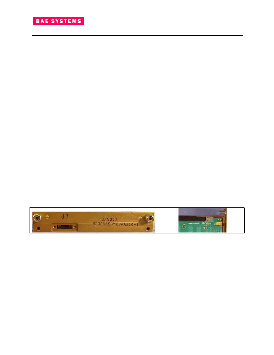
BAE SYSTEMS RAD750 boards are identified by a label on the non-component side of the board near
the front panel, and on the front panel itself. This label gives the revision state of the board, the root code
part number, and the board serial number, etc. as shown in the following diagram:
Figure 3: Board identification label
3.2.3 Malfunction or damage to the board or connected components
Electrostatic discharge and incorrect board installation and uninstallation can damage circuits or
shorten their lifetime.
∑
Before installing or uninstalling the board read this Installation section.
∑
Before installing or uninstalling the board in a CompactPCI rack: - Check all installed boards for
steps that you have to take before turning on / off the power.
∑
Take those steps.
∑
Ensure that the board is connected to the CompactPCI via both the J1 and the J2 connectors and
that the power is available on both CompactPCI connectors.
∑
Finally turn on / off the power.

12
Document #: 234A533
RAD750 3U CompactPCI
Hardware Users Manual
∑
Before touching integrated circuits ensure that you are working in an electrostatic free
environment, and use a tested wrist and heel grounding strap.
3.3 Warnings
Do not exceed the maximum rated input voltages or apply reversed bias to the assembly. If such
conditions occur, toxic fumes may be produced due to the destruction of components.
Only use the RAD750 board in backplanes that supply power on both J1 and J2 connectors. Failure to
observe this warning may result in damage to the board.
3.4 CompactPCI Connector Keying
According to the CompactPCI Specification 2.0, R2.1, boards are marked and keyed according to their
slot type and power supply voltages. The RAD750 board is keyed as a 3.3V signaling I/O board. The
RAD750 board will operate in any CompactPCI slot.
3.5 Insertion Levers/ Jack Screws
The RAD750 board comes with insertion jacks and a front panel. Exercise caution when applying
pressure to the levers during board insertion. Improper seating of the board will cause pin damage on the
J1 and J2 CompactPCI connectors. When plugging the board in or out, do not press at the front panel,
otherwise the front panel can be damaged. Use the handle for plugging the board in or out.
With or without insertion levers, do not apply more than
TBD
pounds of force when inserting this
card in a CompactPCI rack.
3.6 Wedgelocks
The RAD750 board is a conduction-cooled design, utilizing industry standard, multiple segment,
wedgelock retainers and stiffeners. The RAD750 board may be operated without the wedgelocks and
stiffeners and plugged into any commercial CompactPCI rack. The wedgelocks and stiffeners can be
removed by simply unscrewing them. When using a board with the wedgelocks, make sure that the
wedgelocks are tightened down properly. Wedgelocks should be tightened with a torque wrench to
TBD
pounds of torque. When using a board without the wedgelocks mounted, make sure there is sufficient
cooling so that the components are not damaged.
3.7 Power Requirements
The RAD750 board operates on a single +3.3V power supply and is keyed for operation in a 3.3V
signaling CompactPCI system. The Power supply for the box must be capable of supplying at a minimum
of 4.0 A, plus any additional 3.3V power (or other voltages) for other boards in the unit. The voltage
should be highly regulated to a worst case of
±
10% (+/-5% recommended).
The operating temperature of the board is -55
∞
C to +70
∞
C (5% to 95% noncondensing humidity). The
operation of the RAD750 board at the maximum operating temperature requires a minimum airflow of 300
LFM (linear feet per minute) if operated without the wedgelocks installed.
3.8 Backplane Design Guidelines
The RAD750 board is fully compliant with the CompactPCI J1 pin assignments as called out in the
CompactPCI Specification 2.0, R2.1. The RAD750 board connects B09 on J1 to the PCI_RDY_PAR
Sideband Signal from the Power PCI bridge, which is currently specified as reserved. This signal was
added for increased fault tolerance and complies with the PCI specification for sideband signals. Boards
and devices that do not utilize this signal need not connect to B09.

13
Document #: 234A533
RAD750 3U CompactPCI
Hardware Users Manual
3.9 Power-up and Operational Description
This chapter describes power-up and subsequent operation of the RAD750 board.
3.9.1 Power-up
Having configured the backplane and taken note of the system configuration suggestions previously, with
the RAD750 board firmly secured in the rack, power-up the rack.
The SUROM for the RAD750 board, which controls its operation after power-up, is described in the
RAD750 Software Reference Manual.
3.9.2 Operation Description
The POR signal into the processor board must be held active while power is applied. The POR signal to
the processor board will result in an automatic hardware flush reset of the ASIC's, leaving them in their
default state. The EMC in the Power PCI will then take over operational control of the board to run the
desired initialization steps programmed into SUROM (checkout of CPU, Initialization of key structures
such as PCI address and control registers, etc.). The EMC will then hand-off control of the initialization to
the RAD750 CPU by releasing the reset line to the processor. The code that will be run by the EMC as
well as the code run by the processor are programmable and may be different for each mission.
3.9.3 Resetting the RAD750 board
The following section will briefly describe each of the resets available on the RAD750 CompactPCI card.
These resets are:
∑
Power on Reset
∑
PCI Reset
∑
JTAG TRST
∑
JTAG Reset
∑
Software Activated Reset ≠ RAD750
∑
Software Activated Reset ≠ Card
∑
Internal Hardware Critical Error Reset
∑
Built In Self Test (BIST) Reset
The above reset types are the basic types of reset classes for the board from a hardware perspective.
Software can also provide some tailored Reset options through the use of leaving fingerprints in memory
prior to reset or through looking at the state of Programmable Interrupts and Discretes (PIDS) into the
card to select different grouping of instructions to be run during bring-up following a reset.
During a speed change to the RAD750, the bridge chip will generate a HRESET signal to the RAD750
(not SRESET). No PCI reset will be issued since that bus is not effected.
The source of the reset is recorded in the BIST Core Status register that will not be flushed on reset.
Bits 4:0 of this register will be set to indicate the source of the reset as follows:
∑
Bit 4: Logic BIST
∑
Bit 3: JTAG SW Reset
∑
Bit 2: Power PCI internal bus Software Reset (soft reset)
∑
Bit 1: Internal Hardware Reset (Critical Error)
∑
Bit 0: POR

14
Document #: 234A533
RAD750 3U CompactPCI
Hardware Users Manual
3.9.3.1 Power on Reset
A Power on Reset is caused by either the POR signal from the backpanel or the Reset signal from the J7
test connector being activated. This reset causes a flush-reset of all the registers in the Power PCI to
their Reset Value and all outputs will be placed in a safe state as documented in the RAD750
CompactPCI Board Hardware User's manual. The HRESET signal to the RAD750 is also activated
during POR. After the flush reset completes, the Power PCI is then used to check out board health and
reinitialize the chip (dependent on how Power PCI code is written). Control is generally then passed to
the RAD750 to complete the bring-up sequence.
3.9.3.2 PCI Reset
When the Power PCI is configured as PCI central resource (primary input CENTRAL_RESOURCE = `1')
the Power PCI holds PCI_RESET# active while in the Power On Reset state and until the PCI Bus Reset
bit of the PCI Bus Reset register is cleared. When the Power PCI is not the central resource
PCI_RESET# is an input to the Power PCI and reset some of the PCI logic but not the entire Power PCI.
The Power PCI generates PCI RST# when it is configured as central resource and POR or BIST is active,
or the PCI Reset Active bit is set in the Bus Reset register.
The PCI Reset Active bit is read/write from the both the PCI and Power PCI internal bus interfaces in
Power PCI Internal register space. Additionally, this bit is set automatically under any of the following
conditions:
∑
A Data Phase Timeout is detected
∑
An Arbitration Latency Timeout is detected
The PCI Reset Active bit is set to `1' on a flush reset.
Once this bit is set (and RST# is active), it can only be reset via the Power PCI internal bus interface. It is
software's responsibility to ensure that the 1ms minimum reset requirement of the PCI Specification is
met.
With the exception of external I/O tri-state control, the Power PCI responds to a PCI reset in the same
manner, whether it is generating it, or responding to it.
PCI reset is handled as a broad side reset in the Power PCI, and has the following affects:
∑
All PCI defined registers are reset to the states required by the PCI Specification.
∑
All non-PCI defined internal registers remain unchanged.
∑
All PCI state machines are returned to their idle states.
∑
The Power PCI internal bus Master completes its current transaction(s) and then terminate.
∑
All internal buffers are invalidated with the exception of Power PCI internal bus reads and writes
of PCI internal register space.
During a PCI reset, the Power PCI internal bus has access to the PCI internal register space. However,
the PCI defined registers will be held reset as long as PCI RST# is active, so writes to these registers
have no affect.
Any attempted Power PCI internal bus access other than to PCI internal register spaces during a PCI
reset causes an Invalid Power PCI internal bus access error. This results in error signaling back to the
Power PCI internal bus, the setting of the Invalid Power PCI internal bus Access bit in the Status 2
register, and the INTERRUPT_OUT signal going active if not masked in the Status 2 Mask register.
3.9.3.3 JTAG TRST
The Power PCI tri-states its Master JTAG Tap-Reset outputs (JTM_TRST_L and JTMS_TRST_L) while
in the Power on Reset state. JTM_TRST_L and JTMS_TRST_L will be pulled down on card to force the

15
Document #: 234A533
RAD750 3U CompactPCI
Hardware Users Manual
JTAG interface of attached ASICs into the Test-Logic-Reset state during POR and anytime TRST_L is tri-
stated. When JTMS_TRST_L is active the Power PCI's JTAG slave port will be forced to the Test-Logic-
Reset state. This signal has no effect on any other Power PCI logic.
3.9.3.4 JTAG Reset
The Power PCI can be reset via the JTAG slave interface by using the clock control instruction (op code =
`010') and JTAG Address (2:0) = `011'. This Reset is identical to a Power on Reset.
3.9.3.5 Software Activated Reset - RAD750
The Power PCI bridge chip also contains a RAD750 Discretes register which can be to initiate a HRESET
signal to the RAD750 by setting bit 0 of the register. This register can be used as part of error recovery
routines, clock change routines, etc. as determined by the application.
3.9.3.6 Software Activated Reset - Card
In addition, a write to 0x`BF86 0040' from any of the interfaces initiates a full reset of Power PCI.
3.9.3.7 Internal Hardware Critical Error Reset
When the Power PCI internal logic generates a critical error, the Power PCI attempts to handle the error
via vector interrupt 7. If the Power PCI cannot successfully resolve the error condition, it will issue a
software reset. If the internal error prevents the Power PCI from accessing memory, the Power PCI's
Watchdog timer expires, causing an internal hardware generated reset.
3.9.3.8 Built In Self Test (BIST) Reset
The Power PCI enters the BIST Reset state just before exiting BIST. Only bistable logic will be reset
during BIST reset. During BIST reset the Power PCI initializes all internal registers to their Reset Value
with the exception of the Clock and Test registers and the JTAG Tap Controller.
3.10 Troubleshooting
This chapter gives some suggestions for what to do when your RAD750 board doesn't work.
Don't panic!
Use a step-by-step method for looking at the problem.
Try to diagnose the problem type (i.e., hardware or software).
If all else fails, phone or fax your nearest BAE SYSTEMS technical support office for assistance.
3.10.1.1 Step 1- No Power
Check that your enclosure's mains power lead is plugged into the main outlet and into the chassis.
Remove the board during the remainder of the power debug procedure.
Check that you have switched on at the mains and at the system.
Check that you are receiving power from the main outlet (test this with a lamp for example).
Ensure that no fuses have blown.
If the system refuses to start up, this suggests a problem with the power supply. It is essential that only
qualified personnel deal with the problem from now on.

16
Document #: 234A533
RAD750 3U CompactPCI
Hardware Users Manual
3.10.1.2 Step 2 - Power On, Unexpected Behavior
Power the equipment off.
Ensure that the board is firmly seated and secured in the rack and that all male/female connectors mate
together correctly.
Check the links on the board and the system backplane.
If you are unsure of which link configuration to use, use the default configuration initially.
Check that the CompactPCI rack has diode terminators, if these are not built in (the manual for your rack
should tell you whether the terminators are built in).
Check that the power supply is within CompactPCI limits on +3.3V, +5V, +12V and -12V with a digital
voltmeter. Note: The RAD750 board only operates on +3.3V.
Check that there is only one board configured as system controller and that this is in the slot keyed to
receive it.
Check that there are no vacant slots in the rack without jumpers (or that an automatic daisy chaining
backplane is being used).
If you are still getting unexpected behavior, try removing all other CompactPCI boards from the rack and
proving the RAD750 board's operation in isolation, then adding a board at a time until the offending
element is found.
3.10.1.3 Step 3 - Power On, No Terminal Display on the Support Equipment
Check that all cables are plugged in correctly.
If you have made your own cable, check that the pinout and wiring is correct. Note that the Rx and Tx
lines are switched in the cable. See Section 5.2for a description of the cable.
Check that all connections are tight.
Check that the terminal is receiving power and is on.
Check that the terminal is set up for DTE (56 Kbaud, 8 bits/character, 1 stop bit, parity disabled).
3.10.1.4 Step 4 - Overheating
Check that no grilles are blocked in the chassis, either internally or externally.
Check that the fans are working.
Clean or replace any air filters fitted to fans.
Check that there is a free airflow around the chassis exterior (i.e., it should not be in an alcove or other
confined space, or on a thick pile carpet).
Check that the enclosure is not next to a radiator or other heat source.
3.10.1.5 Step 5 - RAD750 board Locks up
Try resetting the RAD750 board or powering the system down and then up again.
3.10.2 Debugging
When debugging software, disable the caches to make tracing the software execution easier.
17
Document #: 234A533
RAD750 3U CompactPCI
Hardware Users Manual
3.11 RAD750 Board Electrical Connectors
The J1 and J2 connectors load a shield at row F on the board. This shield covers the top of the IEC-1076
connector and help to provide a low impedance return path for ground between the board and the
CompactPCI backpanel. The lower shield option that is provided for in IEC-1076 is not required and is
not loaded if it protrudes into the interboard separation plane. Descriptions of the signals on the two
connectors can be found in Section 5.
3.11.1 J1 Connector Pin Assignment
The J1 connector is the primary bus interface for the RAD750 board to the assembly it resides in. The
main PCI and backpanel JTAG signals are mostly routed on this connector. The following color coding is
used in Table 5 and Table 6:
Black - Power and Ground Assignments
Red - Base CompactPCI 32 bit System Mappings
Blue - Fully Compliant Mappings to Unused 64-bit System Signals
Green - Mapping onto Reserved Signals
Purple - Unused Reserved Signals
Table 5 - CompactPCI J1 Connector Signals
PIN
A
B
C
D
E
25
5V
REQ64#
ENUM# -
PID20
3.3V
5V
24
AD1
5V
V(I/O)
AD0
ACK64#
23
3.3V
AD4
AD3
5V
AD2
22
AD7
GND
3.3V
AD6
AD5
21
3.3V
AD9
AD8
GND
C/BE0#
20
AD12
GND
V(I/O)
AD11
AD10
19
3.3V
AD15
AD14
GND
AD13
18
SERR#
GND
3.3V
PAR
C/BE1#
17
3.3V
SDONE
SBO#
GND
PERR#
16
DEVSEL#
GND
V(I/O)
STOP#
LOCK#
15
3.3V
FRAME#
IRDY#
GND
TRDY#
12-14
KEY AREA
11
AD18
AD17
AD16
GND
C/BE2#
10
AD21
GND
3.3V
AD20
AD19
9
C/BE3#
IDSEL
AD23
GND
AD22
8
AD26
GND
V(I/O)
AD25
AD24

18
Document #: 234A533
RAD750 3U CompactPCI
Hardware Users Manual
PIN
A
B
C
D
E
7
AD30
AD29
AD28
GND
AD27
6
REQ#
GND
3.3V
CLK
AD31
5
BRSV
RDY_PARITY
RST#
GND
GNT#
4
BRSV
GND
V(I/O)
INTP
-PID14
INTS
-PID15
3
INTA# -
PID16 -
UART_OUT2
INTB# -
PID17
INTC# -
PID28
5V
INTD# -
PID29
2
TCK
5V
TMS
TDO
TDI
1
5V
-12V
TRST_L
+12V
5V
3.11.2 J2 Connector Pin Assignments
The J2 connector provides the additional PCI signals for the resource controller and all user-defined pins
to the backpanel.
Table 6 - CompactPCI J2 Connector Pinouts
PIN
A
B
C
D
E
22
GA4
GA3
GA2
GA1
GA0
21
CLK6
GND
CLK7
GAP
JTMS_MSTR_E
N
20
CLK5
GND
UART_RTS_L
GND
UART_CTS_L
19
GND
GND
RSV
UART_RX_DAT
UART_TX_DAT
18
BRSV
I2C_1
I2C_0
GND
NMI
17
BRSV
GND
PRST#
REQ6#
GNT6#
16
ROM_ON_PCI
CHAS_GND_0
DEG# -
PID18
GND
CHAS_GND_1
15
BRSV
GND
FAL# -
PID19
REQ5#
GNT5#
14
B64
B64
PID31
GND
PID30
13
B64
GND
V(I/O)
PID08
PID00
12
UART_OUT1
B64
PID25
GND
PID01
11
B64
GND
V(I/O)
PID09
PID02
10
B64
B64
PID26
GND
PID03
9
B64
GND
V(I/O)
PID10
PID04
8
B64
PID21
PID27
GND
PID05
7
B64
GND
V(I/O)
PID11
PID06
19
Document #: 234A533
RAD750 3U CompactPCI
Hardware Users Manual
PIN
A
B
C
D
E
6
B64
PID22
PID24
GND
PID07
5
B64
GND
V(I/O)
B64
PID12
4
V(I/O)
POR_N
PID23
GND
PID13
3
CLK4
GND
GNT3
REQ4#
GNT4#
2
CLK2
CLK3
SYSEN#
GNT2#
REQ3#
1
CLK1
GND
REQ1#
GNT1#
REQ2#
3.12 CompactPCI Slot Guidelines for Multiprocessor Configurations
The Power PCI Bridge chip designed by BAE SYSTEMS and used on the RAD750 processor card is
enhanced over the commercially available MPC-106 chip to allow the multiple processor cards to be
combined on a single compact PCI backpanel. Cards constructed using the Power PCI Bridge chip can
be used in either a system controller or non-system controller slot without any changes being required to
the card design.
The Power PCI chip on the RAD750 processor board uses the SYS_EN signal from the compact PCI
backpanel to determine if it is to act as the system controller for the backpanel. When this signal is active
(i.e., the card is plugged into slot 0 of a standard CompactPCI backpanel), the Power PCI bridge chip on
the board will act as the controller (arbiter). When acting as controller, the Power PCI will supply and then
release (under SW control) the PCI reset signal to the rest of the backpanel.
Each Power PCI chip contains a set of two Base Address Registers (BARs) which are used as follows:
∑
BAR1 - defines the base address for system memory. Its size is selectable by external chip I/O
pins as 2 GByte, 1 GByte, 512 MByte, or 256Mbyte. Furthermore, an internal Power PCI
configuration register (SM_SIZE) is used to determine the number of 8 KByte pages that are
mapped to the PCI bus. The number of 8K pages ranges from 1 to 32768.
∑
BAR2 - defines the base address for the internally architected Power PCI registers. It defines a 1
MByte PCI Memory region. Write access to the lower half of the BAR2 memory region from the
PCI Bus is enabled by the BAR2_WE bit stored in the PCI configuration space.
The following is an example of the use of the BARs:
∑
BAR1 = 0x'1000 0000' with a window size of 256MB.
PCI requests between 0x'1000 0000' and 0x'1FFF FFFF' are translated to PCI memory (local
memory) requests between 0 and 0x'0FFF FFFF'
∑
BAR2 = 0x'2000 0000'
PCI requests between 0x'2000 0000' and 0x'200F FFFF' are translated to PCI memory
(Power PCI register) requests between 0x'BD80 0000' and 0x'BF8F FFFF'.
The BARs must be set in order to access the Power PCI as a target. Both BARs will reset to a base
address of zero so they must be set to avoid conflicts. The local processor may set the BARs or, once
PCI Reset is removed, other PCI masters may set the BARs using configuration cycles.
Power PCI Bridge chips can be used on designs, such as memory cards, which do not contain a
processor. In these applications, an outside PCI master would generally be used to supply configuration
cycles to configure the BAR registers to the required address range.

20
Document #: 234A533
RAD750 3U CompactPCI
Hardware Users Manual
3.13 Compatibility with RAD6000
The RAD750 processor card is fully compatible with the previous RAD6000 based product set. The
Power PCI Bridge to the PCI bus is backward compatible to the PCI version 2.0 bus used in the
RAD6000 family designs. Any required endian conversions can be controlled by software through the
endian conversion hardware in the Power PCI bridge.
3.14 Front Panel Connector
The J7 Front Panel connector provides all external UART, debug and test signals that are brought out to
the front panel. The front panel connector is wired as shown in Table 7.
The J7 front panel connector is a Nanonics Dualobe two row 25 pin connector.
3.14.1 J7 Pin Assignments
Table 7 - Front Panel Connector J7 Pin Assignments
PIN
Signal
PIN
Signal
1
JTM_TDO
2
JTM_TRST_L
3
JTM_TDI
4
JTM_POWER
5
JTM_TCLK
6
JTM_SRESET_L
7
JTM_TMS
8
JTM_RESET_L
9
CPU_CKSTP_L
10
JT7_MSTR_EN_IN
11
GND
12
GND
13
JTS_TDI
14
UART_RX_DATA
15
JTS_TDO
16
UART_TX_DATA
17
JTS_TMS
18
UART_RTS_L
19
JTS_TCLK
20
UART_CTS_L
21
JTS_PROBE_PR_L
22
JTS_TRST_L
23
GND
24
X_SYS_OSC_SEL_L
25
X_SYS_OSC

21
Document #: 234A533
RAD750 3U CompactPCI
Hardware Users Manual
4 Hardware / Electrical
This section describes the electrical and functional characteristics of the RAD750 board. Included are
descriptions of the RAD750, memory maps, register descriptions, etc. Details in the register section are
predominantly about the Power PCI chip.
4.1 RAD750
The RAD750 is functionally equivalent to the PowerPC 750. Users should refer to Section 8.1 for
information on the PowerPC Users Manual.
This section briefly describes the features and general operation of the RAD750 and provides a block
diagram showing major functional units. The RAD750 is an implementation of the PowerPC
microprocessor family of reduced instruction set computer (RISC) microprocessors. The RAD750
implements the 32-bit portion of the PowerPC architecture, which provides 32-bit effective addresses,
integer data types of 8, 16, and 32 bits, and floating-point data types of 32 and 64 bits. The RAD750 is a
superscalar processor that can complete two instructions simultaneously. It incorporates the following six
execution units:
∑
Floating-point unit (FPU)
∑
Branch processing unit (BPU)
∑
System register unit (SRU)
∑
Load/store unit (LSU)
∑
Two integer units (IUs): IU1 executes all integer instructions. IU2 executes all integer instructions
except multiply and divide instructions.
The ability to execute several instructions in parallel and the use of simple instructions with rapid
execution times yield high efficiency and throughput for RAD750-based systems. Most integer
instructions execute in one clock cycle. The FPU is pipelined, the tasks it performs are broken into
subtasks, then implemented as three successive stages. Typically, a floating-point instruction can occupy
only one of the three stages at a time, freeing the previous stage to work on the next floating-point
instruction. Thus, three single-precision floating-point instructions can be in the FPU execute stage at a
time. Double-precision add instructions have a three-cycle latency; double-precision multiply and
multiply-add instructions have a four-cycle latency.
Figure 4 shows the parallel organization of the execution units (shaded in the diagram). The instruction
unit fetches, dispatches, and predicts branch instructions. Note that this is a conceptual model that
shows basic features rather than attempting to show how features are implemented physically.
The RAD750 has independent on-chip, 32-Kbyte, eight-way set-associative, physically addressed caches
for instructions and data and independent instruction and data memory management units (MMUs). Each
MMU has a 128-entry, two-way set-associative translation lookaside buffer (DTLB and ITLB) that saves
recently used page address translations. Block address translation is done through the four-entry
instruction and data block address translation (IBAT and DBAT) arrays, defined by the PowerPC
architecture. During block translation, effective addresses are compared simultaneously with all four BAT
entries.
The L2 cache is supported with an on-chip, two-way, set-associative tag memory. External, synchronous
SRAMs can then be added for data storage. The external SRAMs are accessed through a dedicated L2
cache port that supports a single bank of up to 1 MByte of synchronous SRAMs. The L2 cache is not
implemented in the RAD750 board.
The RAD750 has a 32-bit address bus and a 64-bit data bus. Multiple devices compete for system
resources through a central external arbiter. The RAD750's three-state cache-coherency protocol (MEI)
supports the exclusive, modified, and invalid states, a compatible subset of the MESI
(modified/exclusive/shared/invalid) four-state protocol, and it operates coherently in systems with four-
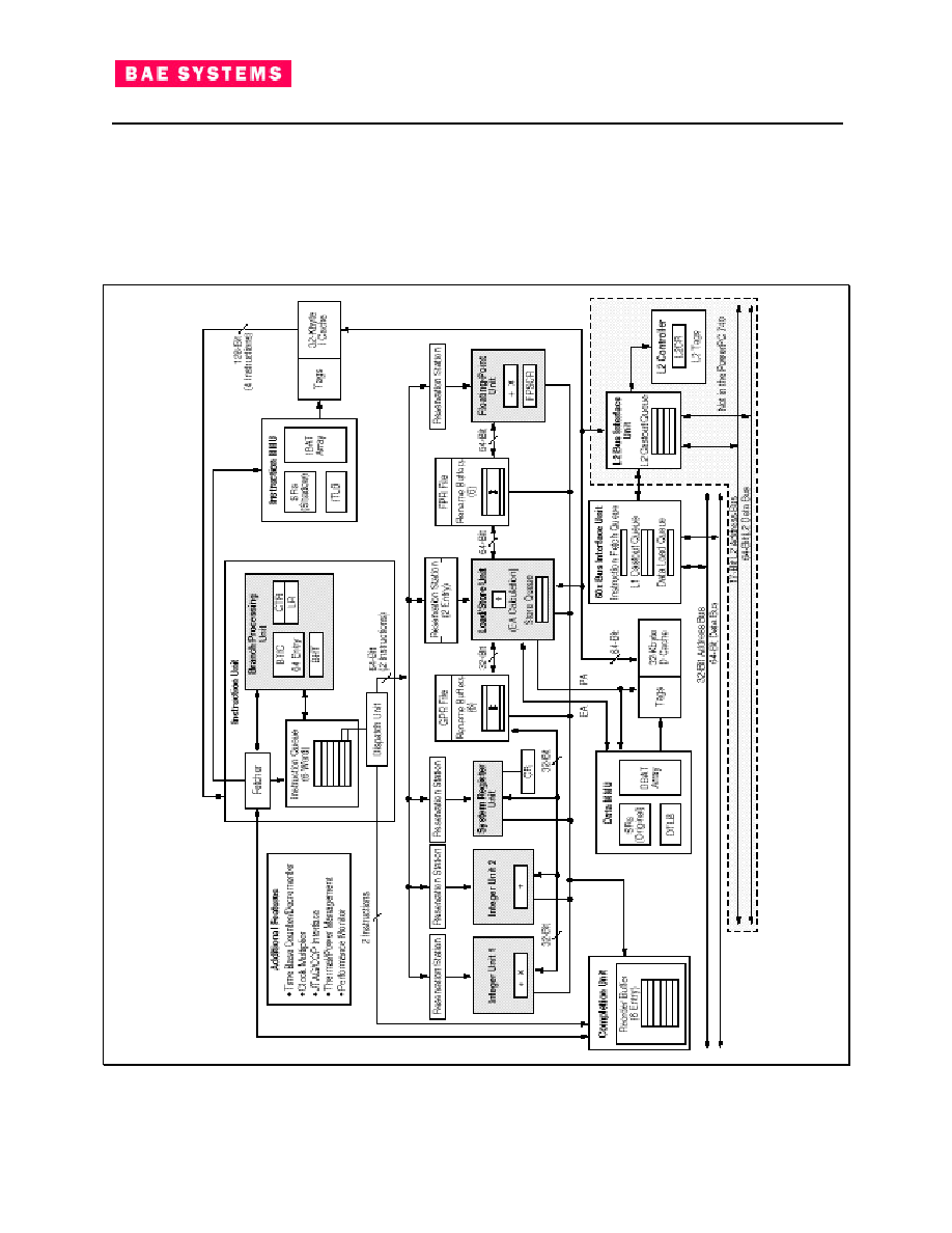
22
Document #: 234A533
RAD750 3U CompactPCI
Hardware Users Manual
state caches. The RAD750 supports single-beat and burst data transfers for memory accesses and
memory-mapped I/O operations.
The RAD750 has four software-controllable power-saving modes. Three static modes, doze, nap, and
sleep progressively reduce power dissipation. When functional units are idle, a dynamic power
management mode causes those units to enter a low-power mode automatically without affecting
operational performance, software execution, or external hardware. The RAD750 also provides a thermal
assist unit (TAU) and a way to reduce the instruction fetch rate for limiting power dissipation.
Figure 4: RAD750 Microprocessor Block Diagram

23
Document #: 234A533
RAD750 3U CompactPCI
Hardware Users Manual
4.1.1 RAD750 Microprocessor Features
This section lists features of the RAD750. The interrelationship of these features is shown in Figure 4.
4.1.1.1 Overview of the PowerPC RAD750 Microprocessor Features
Major features of the RAD750 are as follows:
∑
High-performance, superscalar microprocessor
As many as four instructions can be fetched from the instruction cache per clock cycle
As many as two instructions can be dispatched per clock
As many as six instructions can execute per clock (including two integer instructions)
Single-clock-cycle execution for most instructions
∑
Six independent execution units and two register files
BPU featuring both static and dynamic branch prediction
- 64-entry (16-set, four-way set-associative) branch target instruction cache (BTIC), a
cache of branch instructions that have been encountered in branch/loop code sequences.
If a target instruction is in the BTIC, it is fetched into the instruction queue a cycle sooner
than it can be made available from the instruction cache. Typically, if a fetch access hits
the BTIC, it provides the first two instructions in the target stream.
- 512-entry branch history table (BHT) with two bits per entry for four levels of prediction-
not-taken, strongly not-taken, taken, strongly taken
- Branch instructions that do not update the count register (CTR) or link register (LR) are
removed from the instruction stream.
Two integer units (IUs) that share thirty-two GPRs for integer operands
- IU1 can execute any integer instruction.
- IU2 can execute all integer instructions except multiply and divide instructions (multiply,
divide, shift, rotate, arithmetic, and logical instructions). Most instructions that execute in
the IU2 take one cycle to execute. The IU2 has a single-entry reservation station.
Three-stage FPU
- Fully IEEE 754-1985-compliant FPU for both single- and double-precision operations
- Supports non-IEEE mode for time-critical operations
- Hardware support for denormalized numbers
- Single-entry reservation station
- Thirty-two 64-bit FPRs for single- or double-precision operands
Two-stage LSU
- Two-entry reservation station
- Single-cycle, pipelined cache access
- Dedicated adder performs EA calculations
- Performs alignment and precision conversion for floating-point data
- Performs alignment and sign extension for integer data
- Three-entry store queue
- Supports both big- and little-endian modes
SRU handles miscellaneous instructions
- Executes CR logical and Move to/Move from SPR instructions (mtspr and mfspr)
- Single-entry reservation station
∑
Rename buffers

24
Document #: 234A533
RAD750 3U CompactPCI
Hardware Users Manual
Six GPR rename buffers
Six FPR rename buffers
Condition register buffering supports two CR writes per clock
∑
Completion unit
The completion unit retires an instruction from the six-entry reorder buffer (completion queue)
when all instructions ahead of it have been completed, the instruction has finished execution,
and no exceptions are pending.
Guarantees sequential programming model (precise exception model)
Monitors all dispatched instructions and retires them in order
Tracks unresolved branches and flushes instructions from the mispredicted branch
Retires as many as two instructions per clock
∑
Separate on-chip instruction and data caches (Harvard architecture)
32-Kbyte, eight-way set-associative instruction and data caches
Pseudo least-recently-used (PLRU) replacement algorithm
32-byte (eight-word) cache block
Physically indexed/physical tags. (Note that the PowerPC architecture refers to physical
address space as real address space.)
Cache write-back or write-through operation programmable on a per-page or per-block basis
Instruction cache can provide four instructions per clock; data cache can provide two words
per clock
Caches can be disabled in software
Caches can be locked in software
Data cache coherency (MEI) maintained in hardware
The critical double word is made available to the requesting unit when it is burst into the line-
fill buffer. The cache is nonblocking, so it can be accessed during this operation.
∑
Level 2 (L2) cache interface (The L2 cache is not implemented on the RAD750 board.)
On-chip two-way set-associative L2 cache controller and tags
External data SRAMs
Support for 256-Kbyte, 512-Kbyte, and 1-Mbyte L2 caches
64-byte (256-Kbyte/512-Kbyte) and 128-byte (1 MByte) sectored line size
Supports flow-through (register-buffer), pipelined (register-register), and pipelined late-write
(register-register) synchronous burst SRAMs
∑
Separate memory management units (MMUs) for instructions and data
52-bit virtual address; 32-bit physical address
Address translation for 4-Kbyte pages, variable-sized blocks, and 256-Mbyte segments

25
Document #: 234A533
RAD750 3U CompactPCI
Hardware Users Manual
Memory programmable as write-back/write-through, cacheable/non-cacheable, and
coherency enforced/coherency not enforced on a page or block basis
Separate IBATs and DBATs (four each) also defined as SPRs
Separate instruction and data translation lookaside buffers (TLBs)
- Both TLBs are 128-entry, two-way set associative, and use LRU replacement algorithm
- TLBs are hardware-reloadable (that is, the page table search is performed in hardware)
∑
Separate bus interface units for system memory and for the L2 cache
Bus interface features include the following:
- Selectable bus-to-core clock frequency ratios of 2x, 2.5x, 3x, 3.5x, and 4x
- A 64-bit, split-transaction external data bus with burst transfers
- Support for address pipelining and limited out-of-order bus transactions
- Single-entry load queue
- Single-entry instruction fetch queue
- Two-entry L1 cache castout queue
- No-DRTRY mode eliminates the DRTRY signal from the qualified bus grant. This allows
the forwarding of data during load operations to the internal core one bus cycle sooner
than if the use of DRTRY is enabled.
L2 cache interface features (The L2 cache is not implemented on the RAD750 board) include
the following:
- Core-to-L2 frequency divisors of 1, 1.5, 2, 2.5, and 3
- Four-entry L2 cache castout queue in L2 cache BIU
- 17-bit address bus
- 64-bit data bus
∑
Multiprocessing support features include the following:
Hardware-enforced, three-state cache coherency protocol (MEI) for data cache.
Load/store with reservation instruction pair for atomic memory references, semaphores, and
other multiprocessor operations
∑
Power and thermal management
Three static modes, doze, nap, and sleep, progressively reduce power dissipation:
- Doze - All the functional units are disabled except for the time base/decrementer
registers and the bus snooping logic.
- Nap - The nap mode further reduces power consumption by disabling bus snooping,
leaving only the time base register and the PLL in a powered state.
- Sleep - All internal functional units are disabled, after which external system logic may
disable the PLL and SYSCLK.
Thermal management facility provides software-controllable thermal management. Thermal
management is performed through the use of three supervisor-level registers and an
RAD750-specific thermal management exception.
Instruction cache throttling provides control of instruction fetching to limit power consumption.
∑
Performance monitor can be used to help debug system designs and improve software efficiency.
∑
In-system testability and debugging features through JTAG boundary-scan capability
4.2 Power PCI
The Power PCI ASIC is the single support chip required on the System Flight computer card. It provides
the bridge from the 60X processor bus to local memory, SUROM, and a 3.3V 32-bit PCI interface

26
Document #: 234A533
RAD750 3U CompactPCI
Hardware Users Manual
(compatible with the compact PCI standard). It has a 16550 compatible UART, and 1149.1a JTAG
master and slave interfaces.
Figure 5: Power PCI Chip on a Processor
Board
The Power PCI was designed to support
embedded space applications and thus it has
features such as timers, programmable discrete
I/O, a programmable interrupt controller, and a
simple embedded microcontroller for functions
including fault handling and recovery.
The Power PCI ASIC operates at 33 MHz for the
majority of its functions and its architecture
supports a 33 MHz PCI bus operating
asynchronous to chip clock frequency.
4.2.1 Environment
A functional block diagram of the Power PCI chip
incorporated onto a processor board is shown in
RAD750
CPU
Power PCI
PCI/Mem.
Bridge
6XX Bus
PCI 2.1
SDRAM
SRAM
OR ROM
33MHz
OSC
UART
T
Clk
Figure 5.
The main function of the Power PCI ASIC is to act as a bridge and single support chip for a PowerPC
processor connected to a PCI bus. Both PowerPC 603 and 740/750 microprocessors are supported by
the Power PCI design. The chip architecture is extremely flexible and supports multiple memory types
and several ECC schemes.
4.2.2 Compliance Summary
The Power PCI supports connection to either a PowerPC 603 or a PowerPC 740/750 processor chip.
The PCI bus interface is compatible with the 2.2 version of the PCI Local Bus specification and the
memory interface is compatible with the JEDEC standard SDRAM Architectural and Operational
Features.
RAD750
CPU
Power PCI
PCI/Mem.
Bridge
6XX Bus
PCI 2.1
SDRAM
SRAM
OR ROM
33MHz
OSC
UART
T
Clk
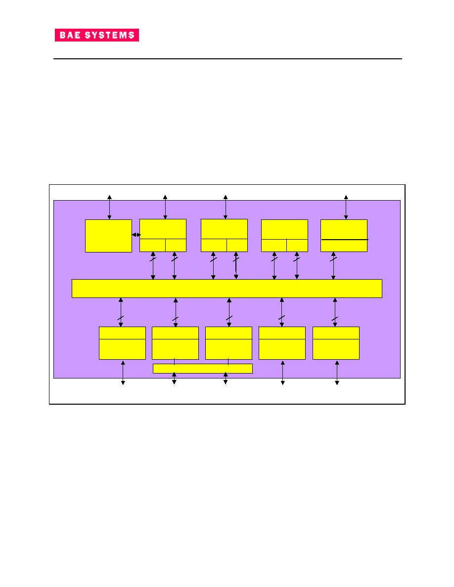
27
Document #: 234A533
RAD750 3U CompactPCI
Hardware Users Manual
4.2.3 Architecture Overview
The Power PCI functions are partitioned into 10 functional blocks or cores. An On-Chip-Bus (OCB) is
used to interconnect all the cores. The OCB is configured as a crossbar switch to prevent the bus from
becoming a performance bottleneck. Each core uses a common OCB interface, known as the OCB stub.
The ten cores are as follows: PCI, P60X, MCC, EMC, CAT, MISC, JTAG Master (two copies), JTAG
Slave, UART, OCB Connection Medium. The P60X, PCI, and EMC cores have both master and slave
capabilities on the OCB and therefore have access to memory and all internal registers excluding the
JTAG Slave registers. The JTAG Slave core is master capable only on the OCB and therefore has
access to memory and all internal registers. The UART, JTAG Masters, MISC, and CAT cores are slave
only on the OCB. All cores except the JTAG's have the capability of generating an interrupt when an
error is encountered or service is required. Core interrupts are collected in the MISC Interrupt Collection
Register and MISC Interrupt Status Register.
JTAG Master
OCB Slave
EMC
OCB
Master
OCB
Slave
PCI
OCB
Master
OCB
Slave
P60X
OCB
Master
OCB
Slave
64
64
64
64
64
64
32
UART
OCB Slave
JTAG Master
OCB Slave
JTAG Slave
OCB Master
Misc
OCB Slave
Clk and Tst
(CAT)
OCB Slave
32
32
32
32
32
OCB Connection Medium
Mem Cntl
Power PCI
Memory I/F
6XX Bus
PCI Bus
JTAG Master
JTAG M/S Slave w
Probe Present
PID's
Clocks/Reset
UART I/F
JTAG M/S Boundary
JTAG M/S Master
Figure 6: Power PCI Cores
4.2.4 Power PCI Features
The Power PCI provides enhanced features over the most used COTS PowerPC bridge chip (Motorola
MPC-106), and thus it is not pin compatible with any COTS bridge chip. The following sections provide
details on the functions contained in the design. Details of the individual register definitions can be found
in the appendix to this document.
4.2.4.1 PCI Bus
The PCI bus interface in the Power PCI ASIC provides a 32-bit PCI master and target interface, and also
includes an optional PCI central resource function. The PCI central resource function is enabled when
the RAD750 3U CompactPCI board is placed in the System Controller slot of a Compact PCI backpanel.

28
Document #: 234A533
RAD750 3U CompactPCI
Hardware Users Manual
The PCI core supports the asynchronous operation of the PCI bus relative to the remainder of the logic
on the RAD750 3U CompactPCI board. Internal buffering of data and command queues is provided.
Some general features the PCI Interface supports are:
∑
32-bit PCI address and data path
∑
0 to 33 MHz operating frequency
∑
Asynchronous application interface
∑
Zero wait-state burst transactions
∑
All types of PCI abort, retry, and disconnect
∑
Delayed transactions
∑
Posted memory writes
∑
Configurable prefetching of read data
∑
64-bit interface to remainder of the RAD750 3U CompactPCI board
A block diagram of the PCI core is shown in Figure 7 and indicates the interconnections between the
various key features in the design.
The PCI core contains User Defined registers known as User Defined Registers A, B, and C. These
registers supply configuration controls to other areas of the Power PCI chip as described in Table 8. In
general, these are used to maintain compatibility with the commercial MPC-106 bridge chip.
PCI Monitor
PCI Arbiter
PCI Initiator
PCI Target
PCI Interface
Internal
Registers
OCB Slave Stub
OCB Master Stub
PCI Boundary
Buffers and Control
PCI
Write
Buffer
PCI
Read
Buffer
OCB
Read
Buffer
Buffer
Control
OCB
Write
Buffer
All Blocks
PCI Bus
OCB Bus
PCI
Core
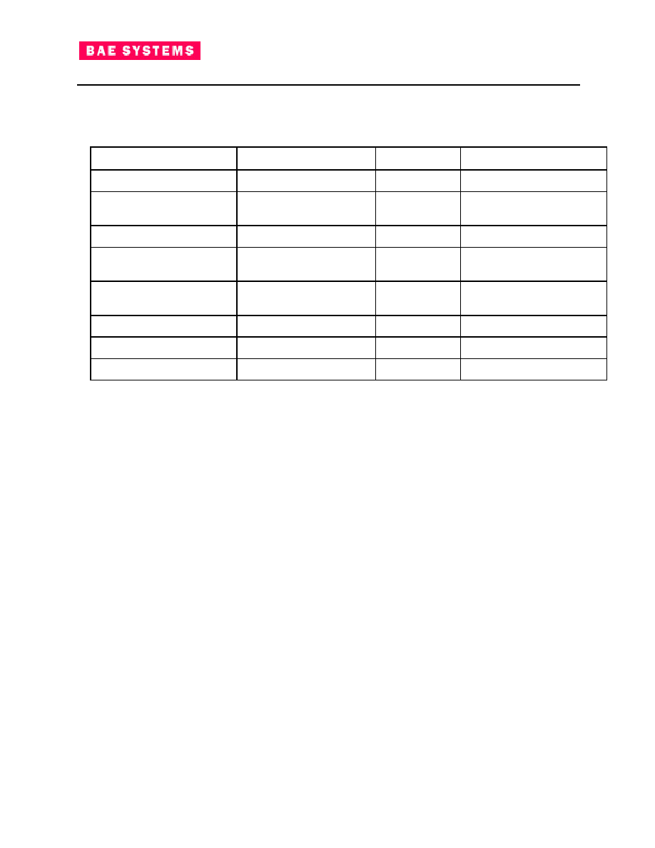
29
Document #: 234A533
RAD750 3U CompactPCI
Hardware Users Manual
Figure 7: PCI Core Block Diagram
Table 8 - PCI User Defined Register Definitions
Bits
Function
Destination
Comments
USER_DEFINED_A(0)
P60x_ERROR_EN
60x Core
60X bus error enable
USER_DEFINED_B(11)
MISC_MCP_ENABLE
Misc Core
Machine Check Interrupt
Enable
USER_DEFINED_B(5)
P60x_ENDIAN_MODE
60x Core
Defines endian mode
USER_DEFINED_C(27)
P60x_NO_SNOOP_EN
60x Core
Enables Snoop on P60X
bus
USER_DEFINED_C(26)
P60x_FF0_LOCAL
60x Core, OCB
Additional SUROM location
control
USER_DEFINED_C(19:18)
P60x_SNOOP_WS
60x Core
Snoop wait states
USER_DEFINED_C(15)
P60x_DBWO_EN
60x Core
Enables DBWO on 60X bus
USER_DEFINED_C(3:2)
P60x_APHASE_WS
60x Core
Address wait states
4.2.4.1.1 PCI Arbiter
When the RAD750 3U CompactPCI board is placed in the system controller slot in a standard Compact
PCI backpanel it will act as the central resource for the PCI bus. As the central resource, the Power PCI
will provide central arbitration for PCI bus accesses. A three level arbitration scheme is used. It is based
on fixed priorities within a level and between levels, but with fairness built in to the two higher priority
levels to ensure that a low priority device is not locked out should higher priority devices continuously
request the bus. Up to eight PCI masters requesting access to the PCI simultaneously is supported. The
Power PCI chip is considered one of these eight masters.
Each of the eight sets of Request/Grant signals can be assigned to one of the three priority levels (or
disabled) using the Arbitration Priority Register in the ASIC. If a request/grant pair were disabled, that
bus master would never be granted the bus. This violates the PCI specification's arbitration fairness
requirement, however it provides the capability for the central resource to turn off an errant master should
that be necessary.
The three arbitration priority levels have fixed priorities in relation to each other with level one having the
highest priority and level three the lowest. Within each level, priorities are also fixed with the lowest order
request having the highest priority. (i.e., If REQ0# and REQ1# are programmed to the same arbitration
level, ARB_REQ0# has higher priority.)
Level one and level two have fairness built in. This means that in addition to all the request/grant pairs
assigned to level one in the PCI Arbitration Priority Level register, level one also contains a level two
fairness chit. The level two fairness chit has lower priority than all other level one requesters, but enables
a lower level requester to be granted the bus before a level one requester that has already used the bus
can be granted the bus a second time. Once one lower level requester has used the bus, all level one
requesters are given the opportunity to take another turn on the bus before the level two fairness chit can
be used again.
Similarly, level two contains a level three fairness chit, allowing one level three device a turn on the bus
after all level two requesters have used the bus. In the case where all level two requesters have already

30
Document #: 234A533
RAD750 3U CompactPCI
Hardware Users Manual
used the bus, and all level one requesters have just finished using the bus, then one device from level
three is allowed to use the bus since both the level 2 and level 3 chits would be active at that time.
The arbiter always grants the bus to the highest priority `non-masked' requester. A requester is masked
by the arbiter as soon as it becomes owner of the bus. A requester becomes unmasked by the arbiter
when there are no longer any unmasked devices at its level requesting the bus ≠ including the fairness
chit. If no devices are requesting the bus, then the arbitration algorithm is essentially reset. So at that
point, if multiple devices request the bus at the same time, the highest priority requester would always be
granted the bus first regardless of previous ownership (or bus parking). Also, note that if only one device
is requesting the bus, it will be granted the bus continuously, until a second device requests the bus (even
though it is still essentially `masked' using the previous definition).
In absence of any active bus requests, the arbiter parks the bus at the last used requester. After reset,
when there is no `last used requester', the PCI Core drives AD(31:0), C/BE(3:0)#, and PAR although the
bus is not actually parked (no GNT(7:0)# is active).
4.2.4.1.2 PCI 2.2 Compliance Summary
The PCI interface is designed to the requirements set forth in the PCI Local Bus Specification, Rev 2.2.
Any and all deviations from the PCI Specification are detailed here. This section does not describe any
optional PCI features that were not implemented.
PCI Specification Chapter 4: Electrical Specification: The PCI logic in the Power PCI chip does not
enforce a minimum length RST# when generating PCI reset as a central resource. Software must adhere
to this PCI requirement.
PCI Specification Chapter 5: Mechanical Specification: These are expansion card requirements and are
dealt with at the card level. The PCI interface contained in the ASIC does not claim compliance to any
requirements in Chapter 5 of the PCI Specification.
PCI Specification Chapter 7: 66 MHz PCI Specification: The current version of the Power PCI dies not
support a 66 MHz PCI. The M66EN signal is not generated by the ASIC.
Transaction Ordering: The PCI core in the Power PCI ASIC can only order transactions with respect to
the OCB interface. It has no knowledge of what goes on beyond the OCB. Therefore, it is possible that
transaction ordering on the entire ASIC device may be violated assuming that there is buffering beyond
the OCB from the PCI core.
SERR#: The PCI Specification defines SERR# as a type O/D signal (i.e., open drain). It only discusses
SERR# as a PCI output. The PCI Core defines this signal as a bi-directional open drain signal so that
when it is acting as the Central Resource on the bus, it can latch an active SERR# input and report it.
When not the central resource, the PCI Core ignores the SERR# as an input.
Subsystem ID: The PCI Specification requires that the Subsystem Vendor ID and Subsystem ID
registers are loaded with valid information prior to any software accessing them in PCI Configuration
Space. The specification suggests responding with Retry on reads to this register until that happens.
The PCI Core allows these registers to be written from the OCB interface, but provides no logic to prevent
the PCI bus from reading these registers prior to that occurring. The PCI Core relies on system specific
software to ensure that this requirement is met.
Transaction Ordering of PCI Configuration Accesses: The PCI Core does not allow PCI configuration
access to participate in transaction ordering. That is, PCI configuration reads and writes can occur
without regard to whether or not data is posted in any of the buffers. The PCI 2.2 Specification implies
that any PCI target read should flush the write buffers, including configuration reads. This `non-
compliancy' precludes the use of the PCI Core internal registers as `flags' for data completion. For
example, if a device were to execute a memory write to the PCI Core which was posted, and then set a
`flag' in one of the PCI Core internal registers, another device could read the `flag' before the posted write
data was written to the OCB. Similarly, a configuration write to a PCI Core internal configuration type

31
Document #: 234A533
RAD750 3U CompactPCI
Hardware Users Manual
register could occur before the posted data was flushed to the OCB, potentially inadvertently modifying
the transfer.
Ordering of Delayed Transactions: The PCI Core in the Power PCI ASIC does not support Rule 5 in
appendix E which states that a Posted Memory Write must be allowed to pass a Delayed Request to
avoid deadlocks. The lack of a retry capability on the OCB interface prohibits adherence to this rule.
However, this rule is stated to prevent a particular deadlock scenario that occurs when a PCI-to-PCI
bridge that supports delayed transactions is used with a PCI-to-PCI bridge that doesn't support delayed
transactions. The PCI Core therefore does not support this configuration.
Memory Write maximum Completion Time Limit: This system level requirement is beyond the scope of
the PCI Interface on the Power PCI chip.
Status Register: The PCI Core enhances PCI error reporting by including the Status 2 register. To
compile all error bits into the same register (the Status 2 register), the PCI Core mirrors bits from the PCI
specification defined Status register into the Status 2 register. By mirroring these bits, the PCI Core
allows some of the Status register bits to be reset by writing `1's to corresponding bit locations in the
Status 2 register. This action may not be considered PCI compliant.
The PCI Specification requires an agent driving data on the PCI bus to drive even parity on PAR. The
Power PCI violates this requirement when OCB or internal register data intended for the PCI bus contains
bad parity. The PCI Core passes the bad OCB or internal register parity on to the PCI. Under normal
conditions (no OCB or internal register parity errors), the PCI Core does pass even parity to the PCI as
required.
1. The PCI Core does not fully support transaction ordering as a PCI Target in that the core does not
prohibit PCI Target reads from completing on the PCI bus when posted OCB Slave write data exists
in the OCB Slave Write Buffer and the OCB Slave write completed on the OCB prior to the PCI
Target read having completed on the OCB.
4.2.4.2 60X Interface
The 60x Bus Interface core contained in the Power PCI (shown in Figure 8) transmits and receives data
between the 60X Bus used by the RAD750, a memory controller interface internal to the Power PCI, and
the Power PCI's internal On Chip Bus (OCB). It provides the bridge from the processor bus to the
memory core as well as the bridge from On Chip Bus to the memory core. Any functional unit master on
the OCB (PCI, JTAG Slave, and EMC) has the capability of accessing the memory core via the 60X core
OCB interface. The 60X core ensures processor cache coherency for these accesses by snooping on
the processor bus. The 60X core also supports functions such as BIST, and boundary scan capabilities.
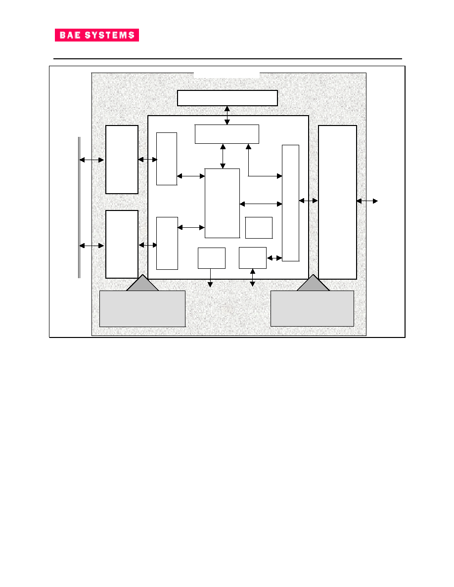
32
Document #: 234A533
RAD750 3U CompactPCI
Hardware Users Manual
OCB
Slave
Stub
I/F
60X Subcore
Boundary
Subcore
OCB
Slave
Stub
Subcore
60X Subcore
To
Boundary Subcore
OCB Slave Stub Subcore
To
60X Subcore
60X CORE
Error /
Misc
CLK
TST
6
0
X
I/
F
OCB
Master
Stub
Subcore
Memory Controller Core
Memory
Request I/F
Endian
Conversion
OCB
Master
Stub
I/F
O
C
B
6
0
X
B
U
S
Config
Registers
Figure 8: 60X Core functional block diagram
The major functions in the 60X core are:
∑
Separate Master and Slave interfaces to the internal Power PCI OCB
∑
60x Subcore
∑
60x Bus Interface
∑
60x Bus Master
∑
60x Bus Slave
∑
60x Bus Arbitrator
∑
Memory Request Interface
∑
Configuration Register Block
∑
Error Interface
∑
Endian Conversion Logic (see Section 4.2.5 for details)
∑
Clock and Test Logic Interface
4.2.4.3 Memory Interface
The Power PCI supports the use of up to 8 banks of memory components though only two banks are
used on the RAD750 3U CompactPCI board. While the 8 banks can be any combination of the three
types of memory (SRAM, PROM/EEPROM, SDRAM), for the RAD750 3U CompactPCI board, Bank 0
contains the 256KB of EEPROM for SUROM and Bank 1 contains the 128MB of SDRAM.

33
Document #: 234A533
RAD750 3U CompactPCI
Hardware Users Manual
The Power PCI is highly configurable via a set of internal registers. Each bank can be programmed for its
error correction mode (SECDED, Parity, and Nibble Correction), timing parameters, etc. Advanced
functions including built in scrubbing and initialization of memory ranges is supported. Sparing of memory
devices for fault tolerance is also supported.
The RAD750 board provides the ability to enable and disable the local and SUROM memory EDAC
mechanisms. The local and SUROM memory EDAC mechanisms are enabled when the board reset.
The RAD750 board provides visibility into the number of memory corrections and address of the
correction. The RAD750 board counts single bit or nibble errors. Multiple bit errors that are
uncorrectable generate a maskable interrupt to the RAD750.
The RAD750 board provides the ability to program different access times for the SUROM and DRAM.
The RAD750 board supports writing to SUROM and Error Injection. Either can be disabled following a
different non-trivial software sequence.
4.2.4.4 JTAG Interfaces
The Power PCI contains three IEEE 1149.1 test ports. The first is a slave port, which can be used to
directly connect the Power PCI to a COT JTAG tester. The next is JTAG master port, which is used to
allow the Power PCI to perform JTAG test and initialization functions on the PowerPC CPU. A `Probe
Connected' signal is provided along with this port to allow the connection to the CPU to be disabled
should the direct connection of a COT JTAG tester to the PowerPC CPU be desired for lab test
operations. The last JTAG port is a combined Master/Slave port, which can be used to incorporate the
Power PCI into a JTAG test ring. In general, this is the port that would be used as the Master JTAG
driving the I/O ASIC JTAG ports in the system.
4.2.4.5 UART
The Power PCI contains a 16550 compatible UART interface. The ASIC itself support the full suite of I/O
signals including: Serial Data In, Serial Data Out, Request to Send (RTS), Clear to Send (CTS), Data Set
Ready (DSR), Data Carrier Detect (DCD), Ring Indicator (RI), Data Terminal Ready (DTR) and two
general purpose output signals. However, four of these signals (DSR, DCD, RI, and DTR) are not
brought off the RAD750 3U CompactPCI board card.
Details on control and usage of the UART function in the Power PCI ASIC can be found in the RAD750
3U CompactPCI board Software User's Manual.
The UART function in the Power PCI contains a Baud Rate Generator that takes a clock input and divide
it by any divisor from 2 to 2
16
-1. This clock is the RTC input to the chip, and for the RAD750 3U
CompactPCI board is the 33 MHz system clock divided by 4, 8, 16, or 32. The output frequency of the
Baud Generator is 16 x the Baud Rate [divisor # = (frequency input) / (baud rate x 16)]. The divisor is
stored in two 8-bit latches called Divisor High Register and Divisor Low. These divisor latches must be
loaded during initialization to ensure proper operation of the Baud Rate Generator. A divisor of zero is
not recommended. Upon loading either of these registers, a 16-bit Baud rate counter is immediately
loaded. Table 9 below shows an example of desired baud rates and their necessary divisors for the four
potential input clock frequencies. The accuracy of the desired baud rate is dependent on the input
frequency chosen and the baud rate. The formula for percent error is as follows: (Input frequency /
Divisor *16) / Desired Baud Rate = Percent Error.

34
Document #: 234A533
RAD750 3U CompactPCI
Hardware Users Manual
Table 9 - UART Baud Rate Programming
8.25 MHz
4.125 MHz
2.0625 MHz
1.03125 MHz
BAUD
RATE
Divisor
(Decimal)
% Error
Divisor
(Decimal)
% Error
Divisor
(Decimal)
% Error
Divisor
(Decimal)
% Error
50
10312
0.005
5156
0.005
2578
0.005
1289
0.005
75
6875
0.000
3437
0.015
1719
0.015
859
0.044
110
4687
0.011
2344
0.011
1172
0.011
586
0.011
134.5
3834
0.009
1917
0.009
958
0.043
479
0.043
150
3437
0.015
1719
0.015
859
0.044
430
0.073
300
1719
0.015
859
0.044
430
0.073
215
0.073
600
859
0.044
430
0.073
215
0.073
107
0.394
1200
430
0.073
215
0.073
107
0.394
54
0.535
1800
286
0.160
143
0.160
72
0.535
36
0.535
2000
258
0.073
129
0.073
64
0.708
32
0.708
2400
215
0.073
107
0.394
54
0.535
27
0.535
3600
143
0.160
72
0.535
36
0.535
18
0.535
4800
107
0.394
54
0.535
27
0.535
13
3.290
7200
72
0.535
36
0.535
18
0.535
9
0.535
9600
54
0.535
27
0.535
13
3.290
7
4.088
19200
27
0.535
13
3.290
7
4.088
3
11.898
28800
18
0.535
9
0.535
4
11.898
2
11.898
38400
13
3.290
7
4.088
3
11.898
2
16.077
56000
9
2.307
5
7.924
2
15.095
1
15.095
128000
4
0.708
2
0.708
1
0.708
n/a
n/a
256000
2
0.708
1
0.708
n/a
n/a
n/a
n/a
4.2.4.6 Timers
The Power PCI contains three identical General Purpose Timers, which are each independently
programmable to support the following functions:
∑
Selectable Up/Down count direction
∑
Selectable External clocking (using a PID) vs. Internal clocking (4 or 8 divide of RTC)
∑
Programmable Reload Value
∑
Reload or hold on terminal count
∑
Interrupt, Discrete output (using a PID) behavior on terminal Count
∑
Capture of timer value in Snapshot register (PID used)
∑
Functional Clear signal (using a PID)
Figure 9 shows a basic block diagram of the General Purpose Timers included in the Power PCI. Each of
the three timers shall be programmable independent of the other two timers.
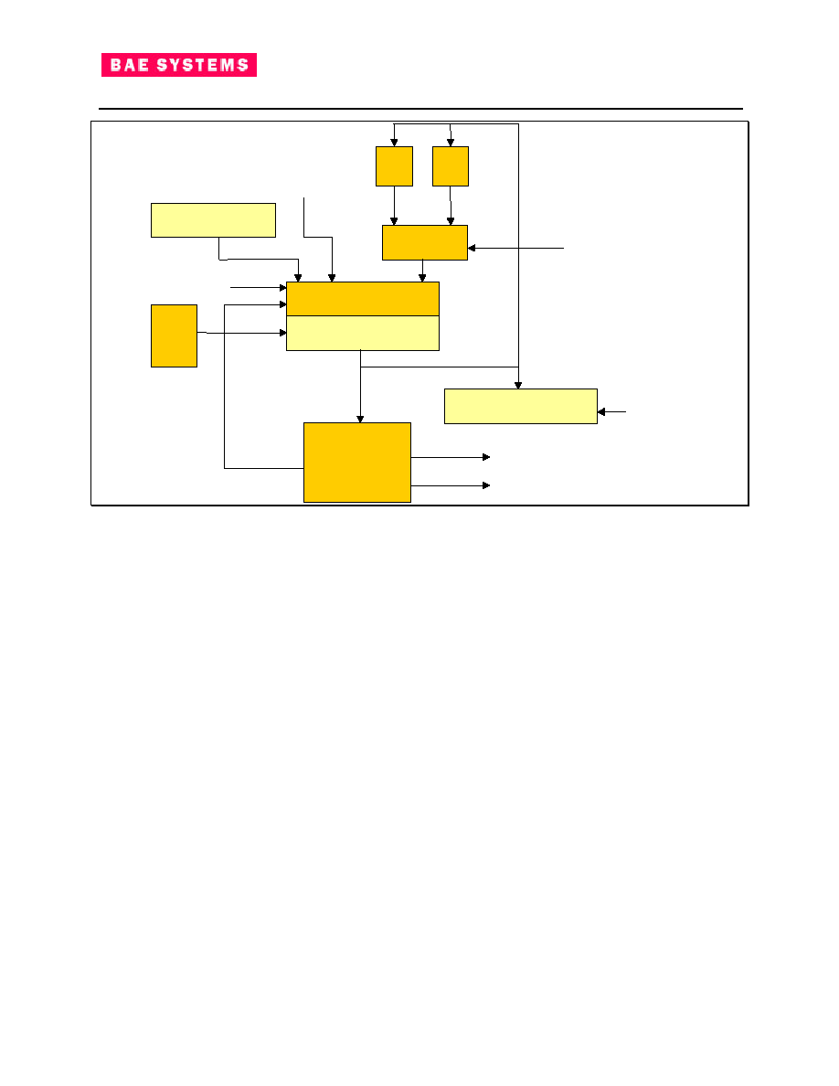
35
Document #: 234A533
RAD750 3U CompactPCI
Hardware Users Manual
Reload Reg
Snapshot Reg
Timer Reg
Select
+1
`0's
-1
Select
Up/Down
Terminal
Detect
Snapshot
Load
Clear
Clk
Sel
Interrupt
Discrete (Pulse or Leve)
Implemantation Note: Reload
Reg and Snapshot Reg are the
same physical register
Figure 9: GP Timer Functional Block Diagram
4.2.4.7 Clock Control
The Power PCI chip contains clock generation logic for the CPU/SDRAM, RTC, JTAG and PCI clocks.
The input source for the clock generation function is either the 33 MHz on-card oscillator input signal
when OSC_SEL is set to `1' or the EXT_OSC input signal when OSC_SEL is set to 0b`0'. Software can
configure the frequency of each clock using the clock generation divide registers. Changes in the divide
frequency of any clock register cause the specified clock set to adjust in a glitch-free-manner to the new
rate. A block diagram of the clock generation function is shown in Figure 10.

36
Document #: 234A533
RAD750 3U CompactPCI
Hardware Users Manual
R
R
R
DIV BY 1/2/4/8
DIV BY 1/2/4/8
DIV BY 4/8/16/32
DELAY
SEL
D
D
D
POWER PCI
PCI LOGIC
33 MHz
OSC
R
D
D
R
SEL
R
POWER PCI
UART & TIMERS
R
D
D
EXT_OSC_SEL
EXT_OSC
PCI_CLK(1:6)
D
PCI_SYSEN#
PCI_CLK(7)
PCI_CLK
RTC_CLK
SYS_CLK
R
DELAY
DELAY
POWER PCI
SYS LOGIC
D
SDRAM
MEMORY
DIV BY 2/4/8/.../256
RAD750
D
D
JTMS_TCLK
DIV BY 2/4/8/.../256
JTAG CLK
SYS CLK
POWER PCI
BRIDGE
X2000
SFC
Figure 10: Clock Generation Logic
The CPU/System clock set generated by the Power PCI consists of three identical signals, each of which
represents the input oscillator frequency divided by either 1, 2, 4, or 8 as determined by the CPU/System
Clock divide register. The first of these signals is connected to the oscillator input to the RAD750 chip
while a second signal is wrapped back to the system clock input to the Power PCI. The third signal is
available to provide a monitor point for lab debug use. These clocks are active in all power saving
modes. The Power PCI is also capable of generating the required control signal sequence to the
RAD750 CPU to safely control it's transitions between clock frequencies and modes. This is described in
more detail in the section on Power Saving Modes of operation.
The RTC Clock set generated by the Power PCI consists of two identical signals, each of which
represents the input oscillator frequency divided by either 2, 4, 8, or 16 as determined by the RTC Clock
divide register. One of these pins is wrapped back to the Power PCI RTC clock input to control the
internal timers, UART, and SDRAM refresh functions. The second signal is available to provide a monitor
point for lab debug use. These clocks are active in all power saving modes.
The PCI Clock set generated by the Power PCI consists of eight identical signals, each of which
represents the input oscillator frequency divided by either 1, 2, 4, or 8 as determined by the PCI Clock
divide register. One of these pins is wrapped back to the PCI clock input to the Power PCI. These clocks
are active in Full, Doze, and Nap modes of operation. In sleep mode, the clocks can be disabled via the
Sleep disable bit in the PCI Clock divide register.
The JTAG clocks are generated off of the internal Power PCI system clock and can be divided by
between 2 and 256.

37
Document #: 234A533
RAD750 3U CompactPCI
Hardware Users Manual
4.2.4.8 Embedded Micro Controller (EMC)
The Power PCI ASIC contains a simple Embedded Microcontroller (EMC) that provides flexibility for
handling reset initialization sequences and error handling functions. The EMC is a RISC based micro-
controller that provides a simple logical, arithmetic, branch, and vector interrupt capabilities. Features of
the EMC include:
32 bit Program Counter
11 General Purpose Registers (GPRs)
5 Special Purpose Registers (SPRs)
8 Vector Interrupts
Full debug facilities
Small Cache (3 cache lines ≠ 32 Bytes each) structure allowing short routines to operate without need of
accessing microinstructions from memory
Microinstruction program control centers around the 32 bit Program Counter. This allows the EMC to
fetch instructions from anywhere within the available address space. In general the Program Counter
increments for each instruction executed unless a branch is specified.
Program execution centers around the 11 32-bit GPR's. Simple logical and arithmetic operations can be
performed on the GPR's along with the ability to load and store them to/from the address space of the
OCB. Initial execution begins at `FFF0 0020'X. This value is parameterizable for the core.
The EMC provides a means to vector program control in order to service critical events in a timely
manner. The Vector Control register contains 8 Vector Pending bits, 8 Vector Enable bits, and 8 Stop
on Vector bits. A Vector Interrupt occurs when one of the Vector Pending bits is set and the
corresponding Vector Enable is set. The EMC enters the Stop state if the corresponding Stop on Vector
bit is also set.
When a Vector Interrupt occurs the EMC saves the current contents of the Program Counter into the
Vector Interrupt Address register and then begin fetching instructions from an indexed location from the
address stored in the Vector Table Anchor register. The Vector Table Anchor register points to 8
consecutive branch instructions, one for each vector. The index for Vector Interrupt 0 is 0, while the index
for Vector Interrupt 7 is 1C hex.
Multiple Vector Interrupts are handled on a priority basis with Vector Interrupt 7 being the highest and
Vector Interrupt 0 being the lowest. When the EMC processes a Vector Interrupt it automatically clears
the Vector Enables for all the maskable Vector Interrupts, thus disabling all Vector Interrupts.
The following lists the microinstructions supported by the EMC sequencer. The valid assignments for the
Source and Destination fields of the instructions are the 11 General Purpose Registers, the
Condition/Status Register, Vector Interrupt Address Register, Vector Control Register, Vector Anchor
Register, Watch Dog Timer, and a zero value.
OR: Dest= Src1 OR Src 2
AND: Dest= Src1 AND Src 2
XOR: Dest= Src1 XOR Src 2
ADD: Dest= Src1 + Src2
ADD Immediate: Dest= Src1 + Immed (immediate data is sign extended to 32 bits)

38
Document #: 234A533
RAD750 3U CompactPCI
Hardware Users Manual
SUB: Dest= Src1 ≠ Src2
SUBI (Sub Immediate): Dest= Src1 ≠ Immed (Immediate data is sign extended to 32 bits)
LD: 32 bit Load to Dest
LDB: 8 bit load, byte determined by 2 lsb's of effective address
LDIU: Load Immediate Upper: Dest(31:16) = Immed
LDIL: Load Immediate Lower: Dest (15:0) = Immed
LDBS: 32 bit load, data byte swapped
LD8: Eight 32-bit loads from 8 consecutive locations into GPR0-7
LD8BS: Eight 32-bit loads from 8 consecutive locations into GPR0-7; Data is byte swapped
ST: 32 bit store
STB: 8 bit store, byte determined by 2 lsb's of effective address
STBS: 32 bit store, data is byte swapped
ST8: Eight 32-bit stores to 8 consecutive locations from GPR0-7
ST8BS: Eight 32-bit stores to 8 consecutive locations in GPR0-7, data is byte swapped
BCI: Branch immediate if condition is true
BNCI: Branch immediate if condition is false
BRI: Branch immediate unconditional
BAL: Branch and Link
Monitor: Enter Monitor State
Stop: Enter Stop State
4.2.4.9 Power Control Modes
The Power PCI supports reduced power operation via its clock control function, however care must be
taken in dividing down clocks in a system where a Power PC based processor is used. The RAD750
contains an internal Phase Lock Loop (PLL) which allows its internal logic to run at a multiplied up value
of its input clock. For example, on the RAD750 3U CompactPCI computer board a 33 MHz clock is sent
to the CPU, which the PLL then multiplies up by 4 to allow the internal logic to run at 133 MHz. It is not
possible to change the input clock rate to the PLL while the PLL is running without potentially damaging
the PLL. However, it is possible to run the CPU with the PLL bypassed and a clock sent directly to it from
outside. It is in this bypass mode that the clock divide power savings features can be used. The Power
PCI is capable of supplying a 4-bit wide PLL configuration bus to the RAD750 to enable and disable the
PLL and to select the multiplier that the PLL will use. For systems requiring less than 60 MIPS, the
processor can be run with the PLL configuration bus always set to disable the PLL. Software can then be
used to divide the input clock rate to the CPU from 33 MHz to a half, fourth, or eighth of this rate. This
can all be done glitch free in virtually the same fashion as the LIO chip. If it is necessary to switch
between having the PLL enabled and bypassed, that can also be accomplished via the Power PCI, but
during the transitioning of the PLL the RAD750 will be held in reset by the Power PCI, meaning the
transition will NOT be glitch free.
In addition to the clock divide power savings modes supported by the Power PCI, it also supports the
PowerPC Nap/Doze/Sleep capabilities. The power management mode is selected by setting the

39
Document #: 234A533
RAD750 3U CompactPCI
Hardware Users Manual
appropriate bits in the Power Management Control Register (configuration offset 70). The bits from this
register that are defined by the Power PCI are:
∑
Bit 7 PM ≠ Power Management Enable
∑
Bit 5 Doze
∑
Bit 4 Nap
∑
Bit 3 Sleep
The power management operational modes for the Power PCI are shown in Table 10. The Power PCI
disables clocks to those internal functions that are not required to be operational during a selected power
savings mode. Each of the operational units in the Power PCI supplies the internal clock function with
status signals indicating when they are busy performing operations and are not capable of entering
reduced power mode. The clock function uses these signals to ensure that the disabling of the clocks to
the shut-off functions does not occur until all on-going operations have completed.
The difference between Doze and Nap is slight, with the only difference being that the chip if the chip is in
Nap mode it will return to full power mode after a 60x bus request. In Doze mode it would return to Doze
rather than going back to full power.
When the Power PCI chip is placed in Nap or Doze mode, various elements have their clocks stopped
internal to the chip. Included in the elements which are stopped are:
∑
60x logic, except for the portion monitoring for bus requests
∑
Memory Interface core logic, except SDRAM refresh and scrubbing
∑
PCI functions ONLY if the source of the PCI clocks in the system disables the clocks
In addition, the lack of transactions occurring from the CPU (and likely the PCI bus) will also cause a
decrease in power simply due to the reduction in internal logic switching factor.

40
Document #: 234A533
RAD750 3U CompactPCI
Hardware Users Manual
Table 10 - Power PCI Power Management Operational Modes
PM Mode
Functioning Units
Activation
Wake Up
Return Mode
Full Power
All
--
--
--
Doze
∑
Same as Nap
Doze bit set
∑
Same as Nap
∑
Doze
Nap
∑
Same as Sleep
∑
PCI target
∑
PCI arbiter
∑
PCI clocks
∑
DRAM Scrub
∑
DRAM refresh (active
or self refresh
supported)
Nap bit set and
assertion of
QREQ
∑
Same as Sleep
∑
PCI target
transaction
∑
60x bus
request
returns to full
power
∑
All others
return to Doze
Sleep
∑
DRAM refresh (Self-
refresh supported)
∑
60x bus request
monitoring
∑
NMI monitoring
∑
Interrupt/Discrete logic
∑
Machine Check
monitoring
∑
JTAG slave
∑
Timers
∑
EMC Vector Interrupt
monitoring
∑
Checkstop Monitoring
∑
PCI Clocks
(Configurable as on or
off)
Sleep bit set
and assertion
of QREQ
∑
Reset
∑
60x bus request
∑
NMI
∑
Interrupt to CPU
∑
Machine Check to
CPU
∑
JTAG slave OCB
access
∑
Internal EMC
Vector Interrupt
∑
Checkstop from
CPU
∑
60x bus
request
returns to full
power
∑
All others
return to
Sleep
4.2.5 Endian Conventions
The Power PCI performs all required endian conversions between interfaces. The following sections
describe how the various `interfaces' will be required to perform endian translations.
4.2.5.1 60x Interface
As done in the MPC-106, a configuration bit can be set as either Big Endian or Little Endian. Memory
accesses coming from the 60x bus must be setup to match this mode and the Power PCI performs a
direct pass of the data internal to the Power PCI. For the remaining interfaces, conversion will be made
depending on the endian mode. If the mode is Big Endian, then the Power PCI performs byte swapping
on the accesses. Otherwise, the Power PCI will unmunge the address. For Big Endian systems, the data
is byte swapped. For Little Endian systems, the address is Munged.
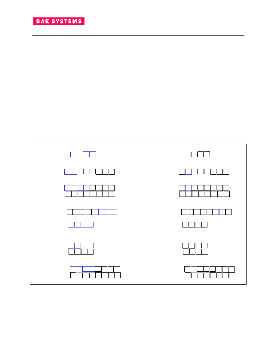
41
Document #: 234A533
RAD750 3U CompactPCI
Hardware Users Manual
4.2.5.2 Memory Interface
It uses memory addresses and stores data unchanged from what is passed to it. It also uses register
addresses and stores data unchanged (Little Endian) from what is passed to it.
4.2.5.3 PCI Interface
The PCI interface is per specification Little Endian, as are its registers, so no byte ordering changes are
be performed.
4.2.5.4 UART
The UART is a simple, byte-oriented interface no endian conversion are required. All accesses are 8 bits
at a time.
4.2.5.5 Power PCI Flow
The following diagrams show how bytes are to be transferred between functions in each of the two endian
configuration. Figure 11 below shows data transfers in Big Endian Mode, and Figure 12 shows data
transfers in Little Endian Mode.
B
Processor
Registers
C
D
A
B
Processor
6xx Bus
C
D
x
A
x
x
x
B
Processor
Memory
C
D
x
A
x
x
x
C
OCB Bus
B
A
D
PLASMA
AMBI, PMBI,
PHASOR,
PMP, QHSS,
BE Targets
r30
0
8
x
x
x
x
x
x
x
x
BL 0 1 2 3 4 5 6 7
BL 7 6 5 4 3 2 1 0
MSB(0)
LSB(3)
MSB(0)
LSB(7)
C
PCI Config.
Registers,
PPCI Regs,
LE Targets
B
A
D
0
4
x
x
x
x
MSB(3)
LSB(0)
B
C
D
x
A
x
x
x
0
8
x
x
x
x
x
x
x
x
MSB(0)
LSB(7)
C
PCI Bus
B
A
D
BL 3 2 1 0
x
x
x
x
B
Processor
Registers
x
x
x
B
Processor
6xx Bus
x
x
x
x
x
x
x
B
Processor
Memory
x
x
x
x
x
x
x
x
OCB Bus
B
x
x
PLASMA
AMBI, PMBI,
PHASOR,
PMP, QHSS,
BE Targets
r30
0
8
x
x
x
x
x
x
x
x
BL 0 1 2 3 4 5 6 7
BL 7 6 5 4 3 2 1 0
MSB(0)
LSB(3)
MSB(0)
LSB(7)
x
PCI Config.
Registers,
PPCI Regs,
LE Targets
B
x
x
0
4
x
x
x
x
MSB(3)
LSB(0)
B
x
x
x
x
x
x
x
0
8
x
x
x
x
x
x
x
x
MSB(0)
LSB(7)
x
PCI Bus
B
x
x
BL 3 2 1 0
x
x
x
x
Figure 11: Data Transfers in Big Endian Mode.
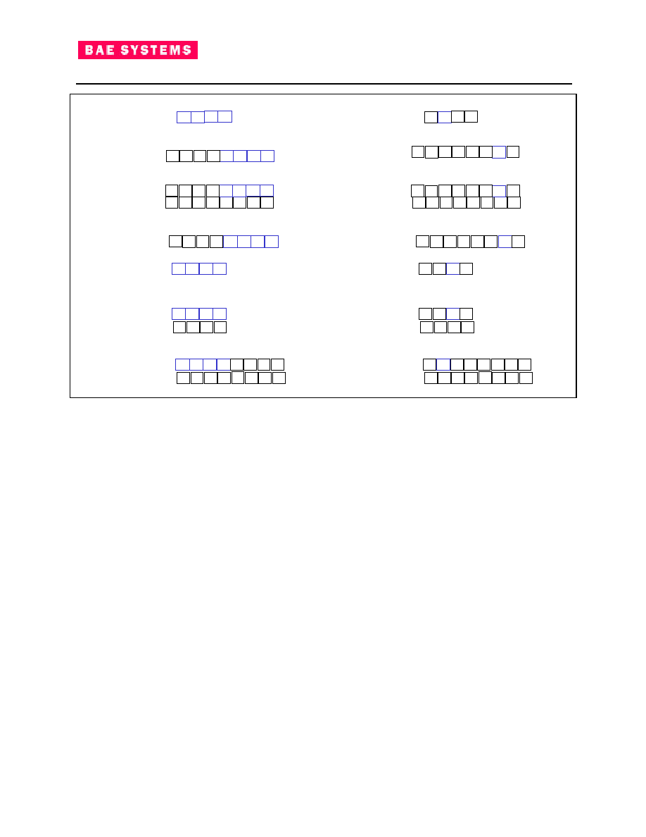
42
Document #: 234A533
RAD750 3U CompactPCI
Hardware Users Manual
B
Processor
Registers
C
D
A
B
Processor
6xx Bus
C
D
x
A
x
x
x
Processor
Memory
B
OCB Bus
C
D
A
PLASMA
AMBI, PMBI,
PHASOR,
PMP, QHSS,
BE Targets
r30
0
8
x
x
x
x
x
x
x
x
BL 0 1 2 3 4 5 6 7
BL 7 6 5 4 3 2 1 0
MSB(0)
LSB(3)
MSB(0)
LSB(7)
B
PCI Config.
Registers,
PPCI Regs,
LE Targets
C
D
A
0
4
x
x
x
x
MSB(3)
LSB(0)
C
B
A
x
D
x
x
x
0
8
x
x
x
x
x
x
x
x
MSB(0)
LSB(7)
B
PCI Bus
C
D
A
BL 3 2 1 0
x
x
x
x
B
Processor
Registers
x
x
x
B
Processor
6xx Bus
x
x
x
x
x
x
x
Processor
Memory
x
OCB Bus
B
x
x
PLASMA
AMBI, PMBI,
PHASOR,
PMP, QHSS,
BE Targets
r30
0
8
x
x
x
x
x
x
x
x
BL 0 1 2 3 4 5 6 7
BL 7 6 5 4 3 2 1 0
MSB(0)
LSB(3)
MSB(0)
LSB(7)
x
PCI Config.
Registers,
PPCI Regs,
LE Targets
B
x
x
0
4
x
x
x
x
MSB(3)
LSB(0)
B
x
x
x
x
x
x
x
0
8
x
x
x
x
x
x
x
x
MSB(0)
LSB(7)
x
PCI Bus
B
x
x
BL 3 2 1 0
x
x
x
x
B
C
D
x
A
x
x
x
B
x
x
x
x
x
x
x
Figure 12: Data Transfers in Little Endian Mode
4.2.6 RAD750 Interrupts and Vector Interrupts
The PowerPC architecture supports a number of interrupt mechanisms to and from the CPU. The
following sections cover each of the mechanisms and describes the use of the interrupt on the RAD750
processor card. The last subsection also describes the use of Vector Interrupts in the Power PCI design.
Vector interrupts are used to signal interrupts to the Embedded Microcontroller (EMC) in the Power PCI
chip for handling.
4.2.6.1 MISC_INT_L (INT)
Source: Power PCI
Destination: RAD750
Description: General Interrupt from Bridge chip to RAD750
The Embedded Programmable Interrupt Collection subfunction in the Power PCI Bridge chip provides for
the collection of interrupts from internal and external sources. It collapses these interrupts into a single
interrupt to the RAD750, MISC_IO_INT_L.
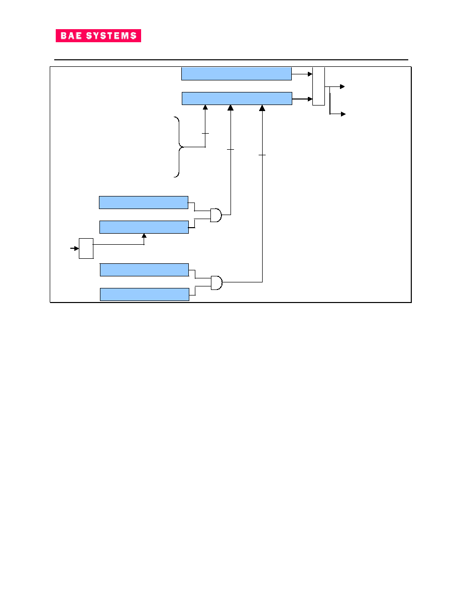
43
Document #: 234A533
RAD750 3U CompactPCI
Hardware Users Manual
AOI
MISC_IO_INT_L
(Interrupt to CPU)
MISC INTERRUPT ENABLE REG(31:0)
MISC INTERRUPT COLLECTION REG(31:0)
PCI Interrupt
60X Interrupt
Mem Cntl High Priority
Mem Cntl Low Priority
UART Interrupt
EMC Interrupt
MISC Interrupt
CAT Interrupt
Power PCI
Core
Interrupts
PID
Cntl
Logic
(31:21)
(15)
1
8
1
(14)
MISC PID VECTOR ENABLE REG(31:0)
MISC PID INPUT REG(31:0)
AO
PID
Interrupt
Multiprocessor
Signaling
Interrupt
MISC SIGNALING ENABLE REG(31:0)
MULTIPROCESSOR SIGNALING REG(31:0)
AO
MISC INTERRUPT
STATUS REG(10)
Figure 13: Power PCI Interrupt Collection
At the top of the interrupt tree is the Interrupt Collection register and the Interrupt Enable register. The
Interrupt Collection register provides status as to the source of an interrupt. Each bit in the Interrupt
Collection register is reduced through an AND-OR function with each corresponding bit in the Interrupt
Enable register to generate the single RAD750 interrupt. Each of the bits in the Interrupt Collection
register represents free running status of the interrupting source. That is when the source of the interrupt
is removed the corresponding bit in the Interrupt Collection register will clear.
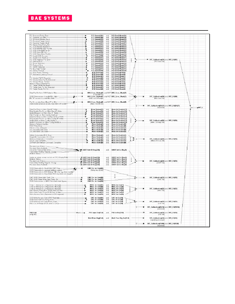
44
Document #: 234A533
RAD750 3U CompactPCI
Hardware Users Manual
Figure 14: Power PCI INT_L Interrupt Tree
The Interrupt Collection register indicates that an interrupt is present at the Power PCI inputs,
MISC_INTERNAL_INT (15:0). MISC_INTERNAL_INT(15:0) is connected to the internal chip interrupt
sources as shown in the following table:

45
Document #: 234A533
RAD750 3U CompactPCI
Hardware Users Manual
Table 11 - Interrupt Register Definition
Bit
Source
Description
15
PCI Bus
PCI Function Interrupt
14
60x Bus
60x Function Interrupt
13:11
Reserved
0b`0'
10
Memory Bus
Memory High Priority Interrupt
09
Memory Bus
Memory Low Priority Interrupt
08
UART
UART Interrupt
07
EMC
EMC Interrupt
06
MISC
Miscellaneous Interrupt
05
CAT
Clock & Test Interrupt
04:00
Reserved
The Interrupt Collection register also provides a bit to indicate that at least one of the Programmable I/O
Discretes (PID), configured as an input interrupt, is active and enabled. The source of this interrupt can
be found in the PID Input register. Each of the PID input interrupts are enabled via the PID Interrupt
Enable register.
The Interrupt Collection register also provides a bit to indicate that at least one of the Multiprocessing
Signaling interrupts is active and enabled. The source of this interrupt can be found in the
Multiprocessor Signaling register. Each of the Multiprocessor Signaling interrupts is enabled via the
Signaling Enable register.
4.2.6.2 NMI_L
Source: PCI Bus (external source)
Destination: Power PCI (then out to RAD750 on MCP error if enabled)
Description: Non-maskable interrupt to CompactPCI Card
The Power PCI chip can receive a non-maskable interrupt (NMI) via the CompactPCI backpanel
connector. This interrupt is active low and will generate a Machine Check to the RAD750, if the Machine
Check interrupt is enabled in the Power PCI bridge chip. See the following section on MCP for more
details.
4.2.6.3 MCP_L
Source: Power PCI
Destination: RAD750
Description: Machine Check Interrupt to RAD750
The Power PCI Bridge chip provides the MCP Collection register that indicates status as to the source of
a Machine Check interrupt. Each bit in the MCP Collection register is reduced through an and-or
function with each corresponding bit in the MCP Enable register to generate the single RAD750 Machine
Check interrupt. Each of the bits in the MCP Collection register represents free running status of the
46
Document #: 234A533
RAD750 3U CompactPCI
Hardware Users Manual
interrupting source. That is when the source of the interrupt is removed the corresponding bit in the MCP
Collection register will clear. The Machine Check interrupt sources is the signals
MISC_INTERNAL_MCP(1:0) and IO_MISC_NMI.
The Machine Check Interrupt is further enabled via the MISC_MCP_ENABLE input. This bit is intended
to be connected (in an MPC-106 compliant bridge chip) to the MPC-106 defined register
PICR1[MCP_EN]. This signal only affects the assertion of the Machine Check Interrupt, not the setting of
bits within the MCP Collection register
PCI User Define B Reg (11)
(Machine Check En)
Rd Data Err on OCB
or
60X_Error_Status(3) and NOT 60X_Error_Mask(3)
or
MCP_Collection(2) and MCP_EN(2)
Data Par Err on OCB
(OCB_MCP)
60x Bus Data Par Err
or
60X_Error_Status(4) and NOT 60X_Error_Mask(4)
60x Bus Addr Par Err
(60X_MCP)
Misaligned 60x transfer
'0'
MCP_Collection(1) and MCP_EN(1)
or
60x APE or DPE received
Par Err from MemCtl I/F
Data Invalid from MemCtl I/F
Retry Error
Invalid Transfer Type
NMI_L
MCP_Collection(0) and MCP_EN(0)
nand
MCP_L
Figure 15: Power PCI MCP Generation Tree
The 60x interface function can send an MISC_INTERNAL_MCP signal to the collection register. The
table below shows the main conditions that will generate the MCP signal. Please note that internal to the
Power PCI, there are two MCP error bits. One if the error was detected on the 60x bus side of the
transfer and another if the error was detected on the Power PCI internal bus side of the transfer.
Table 12 - Error Mechanisms
Error
Detection
Isolation
Reporting
Removal
Recovery
RD Data Error
signal received by
Power PCI internal
bus Master
Subcore
Signal active
Pass Read Data
with Parity
Set "Power PCI
internal bus MCP"
bit in 60x Error
Status Register
Write of "1" to
"Power PCI internal
bus MCP" bit in 60x
Error Status
Register.
External
Data Parity Error in
data read by 60x
Subcore from
Power PCI internal
bus Master
Subcore
Check parity
across data and
data error from
Power PCI
internal bus
Regenerate Parity
on Data
Set "Power PCI
internal bus MCP"
bit in 60x Error
Status Register
Write of "1" to
"Power PCI internal
bus MCP" bit in 60x
Error Status
Register.
External
Received Parity
Error on Data from
60x Bus Interface
Check Parity on
data from 60x
Interface
To Memory: Pass
Data with incorrect
parity;
To Power PCI
internal bus: activate
WR_D_ERR signal;
To internal 60x:
discard data
Set "60x MCP" bit
in 60x Error Status
Register
Write of "1" to "60x
MCP" bit in 60x
Error Status
Register.
External
Received Parity
Error on Address
from 60x Bus
Interface
Check Parity on
address from
60x Interface
Terminate address
transfer by asserting
P60X_IO_ARTRY_L
Set "60x MCP" bit
in 60x Error Status
Register and store
address
information
Write of "1" to "60x
MCP" bit in 60x
Error Status
Register.
External

47
Document #: 234A533
RAD750 3U CompactPCI
Hardware Users Manual
Error
Detection
Isolation
Reporting
Removal
Recovery
Received Illegal
Misaligned transfer
that crosses 32-bit
boundary from 60x
Bus Interface
Check for illegal
misaligned
transfers from
60x Interface
Terminate address
transfer by asserting
P60X_IO_ARTRY_L
Set "60x MCP" bit
in 60x Error Status
Register and store
address
information
Write of "1" to "60x
MCP" bit in 60x
Error Status
Register.
External
Received
IO_P60X_APE
_L or
IO_P60X_DPE
_L is active
Monitor signals
Operation continues
Set "60x MCP" bit
in 60x Error Status
Register
Write of "1" to "60x
MCP" bit in 60x
Error Status
Register.
External
Parity Error on
Data from Memory
Controller Interface
Check Parity on
data from
Memory
Controller
Interface
To Power PCI
internal bus: activate
RD_D_ERR signal;
To 60x: send correct
parity on 60x bus
Set "Memory
Controller Interface
Error" bit in 60x
Error Status
Register;
To 60x: Also Set
"60x MCP" bit in
60x Error Status
Register
Write of "1" to
"Memory Controller
Interface Error" bit
in 60x Error Status
Register.
Write of "1" to "60x
MCP" bit in 60x
Error Status
Register.
External
Data Invalid active
on read data from
Memory Controller
Interface
Monitor Data
Invalid line from
Memory
Controller
Interface
To Power PCI
internal bus: activate
RD_D_ERR signal;
To 60x: send correct
parity on 60x bus
Set "Memory
Controller Interface
Error" bit in 60x
Error Status
Register;
To 60x: Also Set
"60x MCP" bit in
60x Error Status
Register
Write of "1" to
"Memory Controller
Interface Error" bit
in 60x Error Status
Register.
Write of "1" to "60x
MCP" bit in 60x
Error Status
Register.
External
Retry Error
Address on a
retried read to
the Power PCI
internal bus
does not match
the original
address
Operation Continues
Set "60x MCP" bit
in 60x Error Status
Register
Write of "1" to "60x
MCP" bit in 60x
Error Status
Register.
External
Invalid Transfer
Type from the 60x
interface
Check for
invalid Transfer
Type
Terminate Address
transfer by asserting
P60X_IO_ARTRY_L
Set "60x MCP" bit
in 60x Error Status
Register
Write of "1" to "60x
MCP" bit in 60x
Error Status
Register.
External
4.2.6.4 SMI_L
Source: On Card Pull-up
Destination: RAD750
Description: System Management Interrupt
This signal, which is not part of the standard PowerPC Architecture, is not used on the RAD750 3U
CompactPCI board design and is tied inactive on the card.
4.2.6.5 TEA_L
Source: On Card Pull-up
Destination: RAD750

48
Document #: 234A533
RAD750 3U CompactPCI
Hardware Users Manual
Description: Transfer Error Acknowledge
In a commercial PowerPC system, TEA is generally used by a memory controller to signal a memory
parity or uncorrectable ECC error has occurred. The receipt of TEA by the RAD750 generally causes a
Machine Check (or it can cause a fatal Checkstop error). In the RAD750 3U CompactPCI board system
the TEA signal is not used. Rather the internal interrupt gathering mechanisms of the Power PCI are
used to handle memory errors and to signal the RAD750, if desired via the MCP or INT signals.
Therefore, the TEA signal is tied inactive on the RAD750 3U CompactPCI card.
4.2.6.6 RAD750_CKSTP_OUT_L
Source: RAD750
Destination: Power PCI Bridge
Description: RAD750 Checkstop (fatal error signal)
The Checkstop signal from the processor signals that the RAD750 has hit a fatal error and is no longer
operating. This signal is received by the Power PCI ASIC and is mapped to Vector Interrupt #5. It would
generally be expected that the Power PCI routine coded to handle this interrupt level would reset the
RAD750 and perform some form of BIST to determine if a solid failure exists, and if not, it could reinitialize
the RAD750 for continued operation.
The Checkstop signal received by the Power PCI bridge can be masked off as follows. The Power PCI
statuses the state of the primary input IO_MISC_CKSTP_L in the Checkstop bit of the Vector Interrupt
Status register. While the Checkstop bit is active and the corresponding enable in the Vector Interrupt
Enable register is active then the Power PCI activates MISC_EMC_VECTOR_INT(5). The Power PCI
latches the IO_MISC_CKSTP_L signal."
4.2.6.7 RAD750_CKSTP_IN_L
Source: Power PCI Bridge
Destination: RAD750
Description: RAD750 Checkstop (fatal error signal)
The Power PCI activates the primary output MISC_IO_CKSTP_L when a Critical Error bit is active in the
Vector Interrupt Status register, the corresponding bit in the Vector Interrupt Enable register is active,
and the checkstop Enable bit of the RAD750 Discretes register is set. Figure 16 shows the actual logic
tree used in the Power PCI for this function. The Power PCI latches the MISC_IO_CKSTP_L signal.
Sources of critical errors include internal chip errors such as SEU errors causing hot-bit state machines to
be in two states at once, internal bus parity errors, etc. These errors are classified as critical because
they will generally require a reset from the EMC to recover from. The Power PCI chip sends the
Checkstop signal to the RAD750 which will then stop all operation and take place its I/O in high
impedance state (safe mode).
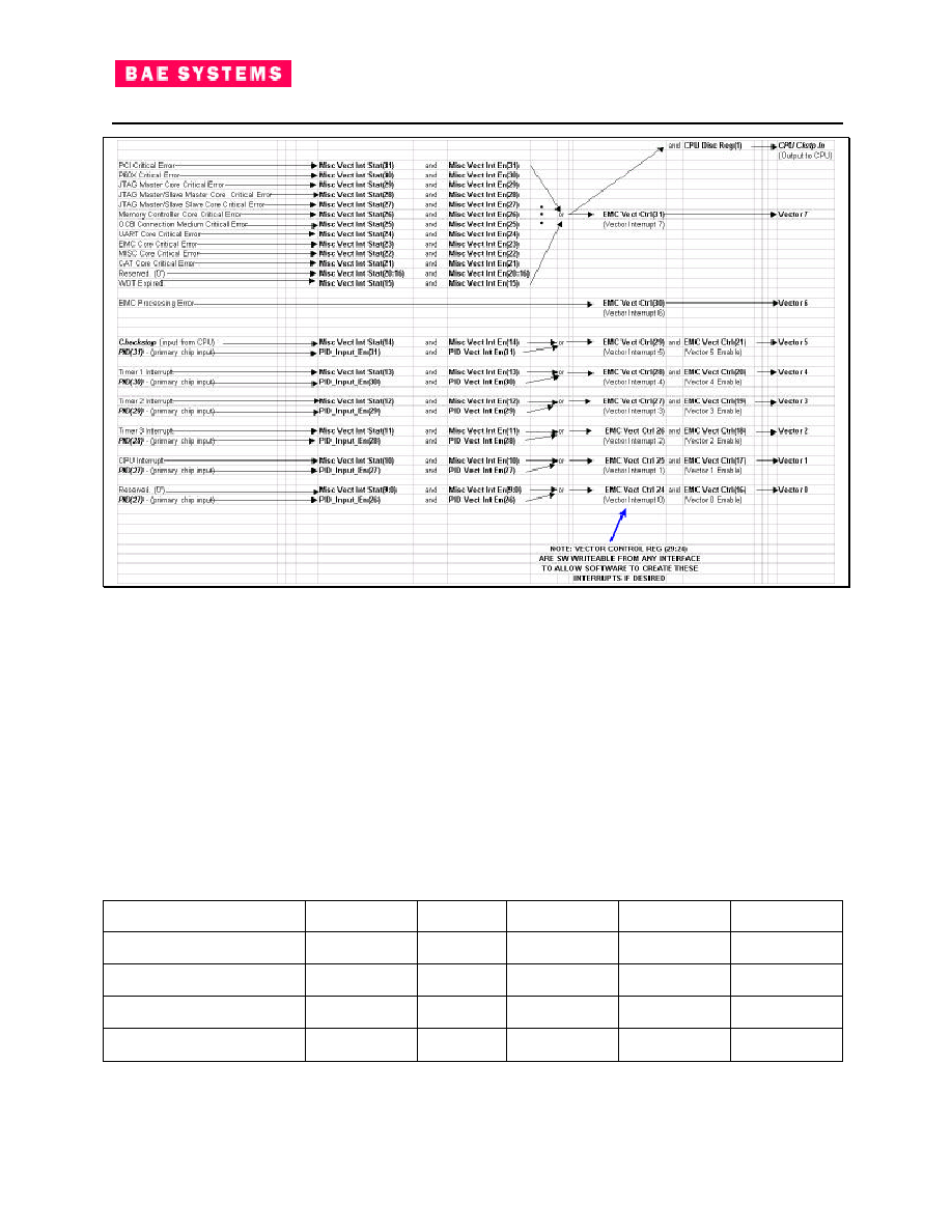
49
Document #: 234A533
RAD750 3U CompactPCI
Hardware Users Manual
Figure 16: Power PCI Checkstop Generation Tree and Vector Interrupt Tree
4.2.6.8 Vector Interrupts
Not all interrupts on the processor card need to be handled by the RAD750. The Power PCI supports the
use of Vector Interrupts, which can be handled by the Power PCI's internal EMC. Figure 16 shows the
interrupt generation tree for these vector interrupts. More details on the Vector Interrupt function of the
EMC can be found in Section 4.2.4.8.
4.2.6.9 Interrupt Latencies
The RAD750 board has the maximum external interrupt latencies while running from local memory shown
in Table 13, depending on mode and speed. Latencies are measured from interrupt signal transition to
first instruction execution of the interrupt handler.
Table 13 - RAD750 board Interrupt Latencies
132 MHz
33 MHz
16.5 MHz
8.25 MHz
4.125 MHz
Full-on Mode (
µ
sec)
10
µ
sec
TBA
TBA
TBA
TBA
Doze Mode (
µ
sec)
TBA
TBA
TBA
TBA
TBA
Nap Mode (
µ
sec)
TBA
TBA
TBA
TBA
TBA
Sleep Mode (
µ
sec)
TBA
TBA
TBA
TBA
TBA
50
Document #: 234A533
RAD750 3U CompactPCI
Hardware Users Manual
5 External Electrical Interface
The following sections provide a consolidated list of Input and Output signals on the RAD750 board.
5.1 CompactPCI Defined Signals
Table 14 shows the PCI bus signals used on the RAD750 3U CompactPCI board.
Table Heading Notes:
In the Signal Type column:
BDTS indicates a bi-directional, tri-state input/output pin (only one direction at a time).
BDODIL indicates a bi-directional, open drain, inverted logic input/output pin, with an external pull-up
resistor, allowing multiple devices to concurrently drive the signal in a "wired-OR" configuration. Drivers
assert the bus (i.e. sink current) to indicate a logic "1" state or release the bus (i.e. tri-state) to indicate a
logic "0" state.
OTS indicates a tri-state output.
OD indicates open drain output with external pull-up resistor allowing multiple devices to share as a wire-
OR.
BDOD indicates a bi-directional, open drain input/output pin.
BDSTS indicates a bi-directional, sustained tri-state. This is an active low tri-state signal owned and
driven by one, and only one, agent at a time. The agent that drives an STS pin low must drive it high for
at least one clock cycle before letting it float. A new agent cannot start driving any sooner than one clock
cycle after the previous owner tri-states it. An external pull-up resistor is required to sustain the inactive
state until another agent drives it.
CS indicates cold-spareable.
SP indicates internal soft pull-up on an input.
The I/O Pin identifies which connector (first two characters) and which pin (last three characters) the
signal is wired to. See section 3.11 for more details on the connectors.
The Voltage/Technology column indicates the type of I/O assumed for signals at the card boundary.
Included here are external non-VLSI elements and terminations.
In the POR Value column, the value shown is the state of the signal after a POR is issued. If a second
value is shown, this is for when the card is being used as a PCI Resource Controller.
In the PCI Reset column, the value shown is the state of the signal after a PCI Reset is issued. If a
second value is shown, this is for when the card is being used as a PCI Resource Controller.
Table 14 - X2000 System Flight Computer PCI Interface Signals
SIGNAL NAME
Signal
Type
I/O
Pin
Voltage/
Technology
POR
Value
PCI Reset
Value
Comment
PCI Bus
PCI_AD_0
BDTS
J1D24
3.3V PCI
5V PCI Toler.
10 Ohm Stub
3-State
3-State / 0
PCI Address/Data Bus

51
Document #: 234A533
RAD750 3U CompactPCI
Hardware Users Manual
SIGNAL NAME
Signal
Type
I/O
Pin
Voltage/
Technology
POR
Value
PCI Reset
Value
Comment
PCI_AD_1
BDTS
J1A24
3.3V PCI
5V PCI Toler.
10 Ohm Stub
3-State
3-State / 0
PCI Address/Data Bus
PCI_AD_2
BDTS
J1E23
3.3V PCI
5V PCI Toler.
10 Ohm Stub
3-State
3-State / 0
PCI Address/Data Bus
PCI_AD_3
BDTS
J1C23
3.3V PCI
5V PCI Toler.
10 Ohm Stub
3-State
3-State / 0
PCI Address/Data Bus
PCI_AD_4
BDTS
J1B23
3.3V PCI
5V PCI Toler.
10 Ohm Stub
3-State
3-State / 0
PCI Address/Data Bus
PCI_AD_5
BDTS
J1E22
3.3V PCI
5V PCI Toler.
10 Ohm Stub
3-State
3-State / 0
PCI Address/Data Bus
PCI_AD_6
BDTS
J1D22
3.3V PCI
5V PCI Toler.
10 Ohm Stub
3-State
3-State / 0
PCI Address/Data Bus
PCI_AD_7
BDTS
J1A22
3.3V PCI
5V PCI Toler.
10 Ohm Stub
3-State
3-State / 0
PCI Address/Data Bus
PCI_AD_8
BDTS
J1C21
3.3V PCI
5V PCI Toler.
10 Ohm Stub
3-State
3-State / 0
PCI Address/Data Bus
PCI_AD_9
BDTS
J1B21
3.3V PCI
5V PCI Toler.
10 Ohm Stub
3-State
3-State / 0
PCI Address/Data Bus
PCI_AD_10
BDTS
J1E20
3.3V PCI
5V PCI Toler.
10 Ohm Stub
3-State
3-State / 0
PCI Address/Data Bus
PCI_AD_11
BDTS
J1D20
3.3V PCI
5V PCI Toler.
10 Ohm Stub
3-State
3-State / 0
PCI Address/Data Bus
PCI_AD_12
BDTS
J1A20
3.3V PCI
5V PCI Toler.
10 Ohm Stub
3-State
3-State / 0
PCI Address/Data Bus
PCI_AD_13
BDTS
J1E19
3.3V PCI
5V PCI Toler.
10 Ohm Stub
3-State
3-State / 0
PCI Address/Data Bus

52
Document #: 234A533
RAD750 3U CompactPCI
Hardware Users Manual
SIGNAL NAME
Signal
Type
I/O
Pin
Voltage/
Technology
POR
Value
PCI Reset
Value
Comment
PCI_AD_14
BDTS
J1C19
3.3V PCI
5V PCI Toler.
10 Ohm Stub
3-State
3-State / 0
PCI Address/Data Bus
PCI_AD_15
BDTS
J1B19
3.3V PCI
5V PCI Toler.
10 Ohm Stub
3-State
3-State / 0
PCI Address/Data Bus
PCI_AD_16
BDTS
J1C11
3.3V PCI
5V PCI Toler.
10 Ohm Stub
3-State
3-State / 0
PCI Address/Data Bus
PCI_AD_17
BDTS
J1B11
3.3V PCI
5V PCI Toler.
10 Ohm Stub
3-State
3-State / 0
PCI Address/Data Bus
PCI_AD_18
BDTS
J1A11
3.3V PCI
5V PCI Toler.
10 Ohm Stub
3-State
3-State / 0
PCI Address/Data Bus
PCI_AD_19
BDTS
J1E10
3.3V PCI
5V PCI Toler.
10 Ohm Stub
3-State
3-State / 0
PCI Address/Data Bus
PCI_AD_20
BDTS
J1D10
3.3V PCI
5V PCI Toler.
10 Ohm Stub
3-State
3-State / 0
PCI Address/Data Bus
PCI_AD_21
BDTS
J1A10
3.3V PCI
5V PCI Toler.
10 Ohm Stub
3-State
3-State / 0
PCI Address/Data Bus
PCI_AD_22
BDTS
J1E09
3.3V PCI
5V PCI Toler.
10 Ohm Stub
3-State
3-State / 0
PCI Address/Data Bus
PCI_AD_23
BDTS
J1C09
3.3V PCI
5V PCI Toler.
10 Ohm Stub
3-State
3-State / 0
PCI Address/Data Bus
PCI_AD_24
BDTS
J1E08
3.3V PCI
5V PCI Toler.
10 Ohm Stub
3-State
3-State / 0
PCI Address/Data Bus
PCI_AD_25
BDTS
J1D08
3.3V PCI
5V PCI Toler.
10 Ohm Stub
3-State
3-State / 0
PCI Address/Data Bus
PCI_AD_26
BDTS
J1A08
3.3V PCI
5V PCI Toler.
10 Ohm Stub
3-State
3-State / 0
PCI Address/Data Bus

53
Document #: 234A533
RAD750 3U CompactPCI
Hardware Users Manual
SIGNAL NAME
Signal
Type
I/O
Pin
Voltage/
Technology
POR
Value
PCI Reset
Value
Comment
PCI_AD_27
BDTS
J1E07
3.3V PCI
5V PCI Toler.
10 Ohm Stub
3-State
3-State / 0
PCI Address/Data Bus
PCI_AD_28
BDTS
J1C07
3.3V PCI
5V PCI Toler.
10 Ohm Stub
3-State
3-State / 0
PCI Address/Data Bus
PCI_AD_29
BDTS
J1B07
3.3V PCI
5V PCI Toler.
10 Ohm Stub
3-State
3-State / 0
PCI Address/Data Bus
PCI_AD_30
BDTS
J1A07
3.3V PCI
5V PCI Toler.
10 Ohm Stub
3-State
3-State / 0
PCI Address/Data Bus
PCI_AD_31
BDTS
J1E06
3.3V PCI
5V PCI Toler.
10 Ohm Stub
3-State
3-State / 0
PCI Address/Data Bus
PCI_C/BE0#
BDTS
J1E21
3.3V PCI
5V PCI Toler.
10 Ohm Stub
3-State
3-State / 0
PCI Cmd/Byte Enable
PCI_C/BE1#
BDTS
J1E18
3.3V PCI
5V PCI Toler.
10 Ohm Stub
3-State
3-State / 0
PCI Cmd/Byte Enable
PCI_C/BE2#
BDTS
J1E11
3.3V PCI
5V PCI Toler.
10 Ohm Stub
3-State
3-State / 0
PCI Cmd/Byte Enable
PCI_C/BE3#
BDTS
J1A09
3.3V PCI
5V PCI Toler.
10 Ohm Stub
3-State
3-State / 0
PCI Cmd/Byte Enable
PCI_PAR
BDTS
J1D18
3.3V PCI
5V PCI Toler.
10 Ohm Stub
3-State
3-State / 0
Even Parity over AD and
C/BE(0:3)#
PCI_FRAME#
BDSTS
J1B15
3.3V PCI
5V PCI Toler.
10 Ohm Stub
8.2K Pull-up
3-State
3-State
Master Start / Stop
PCI_IRDY#
BDSTS
J1C15
3.3V PCI
5V PCI Toler.
10 Ohm Stub
8.2K Pull-up
3-State
3-State
Initiator Ready

54
Document #: 234A533
RAD750 3U CompactPCI
Hardware Users Manual
SIGNAL NAME
Signal
Type
I/O
Pin
Voltage/
Technology
POR
Value
PCI Reset
Value
Comment
PCI_TRDY#
BDSTS
J1E15
3.3V PCI
5V PCI Toler.
10 Ohm Stub
8.2K Pull-up
3-State
3-State
Target Ready
PCI_STOP#
BDSTS
J1D16
3.3V PCI
5V PCI Toler.
10 Ohm Stub
8.2K Pull-up
3-State
3-State
Target Stop
PCI_DEVSEL#
BDSTS
J1A16
3.3V PCI
5V PCI Toler.
10 Ohm Stub
8.2K Pull-up
3-State
3-State
Device select
PCI_IDSEL
Input
J1B09
3.3V PCI
5V PCI Toler.
10 Ohm Stub
N/A
N/A
Chip select for device
configuration space
PCI_PERR#
BDSTS
J1E17
3.3V PCI
5V PCI Toler.
10 Ohm Stub
8.2K Pull-up
3-State
3-State
Parity Error
PCI_SERR#
BDOD
1
J1A18
3.3V PCI
5V PCI Toler.
10 Ohm Stub
8.2K Pull-up
Floated
Floated
System Error
PCI_REQ#
BDTS
1
J1A06
3.3V PCI
5V PCI Toler.
Series Term.
3-State
3-State
Bus Request
PCI_GNT#
BDTS
2
J1E05
3.3V PCI
5V PCI Toler.
Series Term.
100K Pull-up
N/A /
3-State
N/A /
3-State
Bus Grant
PCI_RST#
BDTS
2
J1C05
3.3V PCI
5V PCI Toler.
N/A
/ 0
N/A / 0
Reset
PCI_RDY_PAR
BDTS
2
J1B05
3.3V PCI
5V PCI Toler.
10 Ohm Stub
8.2K Pull-up
N/A /
3-State
N/A /
3-State
Ready Parity
PCI_CLK
BDTS
2
J1D06
3.3V PCI
5V PCI Toler.
Series Term.
N/A /
Active
N/A /
Active
Bus Clock
PCI_SDONE
N/A
J1B17
None
Unused
PCI_SBO#
N/A
J1C17
None
Unused

55
Document #: 234A533
RAD750 3U CompactPCI
Hardware Users Manual
SIGNAL NAME
Signal
Type
I/O
Pin
Voltage/
Technology
POR
Value
PCI Reset
Value
Comment
PCI_LOCK#
N/A
J1E16
10 Ohm Stub
N/A
N/A
Unused
PCI Central Resource
PCI_SYSEN#
Input
J2C02
3.3V PCI
5V PCI Toler.
8.2K Pull-up
N/A
N/A
System Slot Enable
PCI_REQ1#
Input
J2C01
3.3V PCI
5V PCI Toler.
N/A
N/A
Arbitration Request
PCI_REQ2#
Input
J2E01
3.3V PCI
5V PCI Toler.
N/A
N/A
Arbitration Request
PCI_REQ3#
Input
J2E02
3.3V PCI
5V PCI Toler.
N/A
N/A
Arbitration Request
PCI_REQ4#
Input
J2D03
3.3V PCI
5V PCI Toler.
N/A
N/A
Arbitration Request
PCI_REQ5#
Input
J2D15
3.3V PCI
5V PCI Toler.
N/A
N/A
Arbitration Request
PCI_REQ6#
Input
J2D17
3.3V PCI
5V PCI Toler.
N/A
N/A
Arbitration Request
PCI_GNT1#
OTS
J2D01
3.3V PCI
Series Term.
3-State
3-State
Arbitration Grant
PCI_GNT2#
OTS
J2D02
3.3V PCI
Series Term.
3-State
3-State
Arbitration Grant
PCI_GNT3#
OTS
J2C03
3.3V PCI
Series Term.
3-State
3-State
Arbitration Grant
PCI_GNT4#
OTS
J2E03
3.3V PCI
Series Term.
3-State
3-State
Arbitration Grant
PCI_GNT5#
OTS
J2E15
3.3V PCI
Series Term.
3-State
3-State
Arbitration Grant
PCI_GNT6#
OTS
J2E17
3.3V PCI
Series Term.
3-State
3-State
Arbitration Grant
PCI_CLK1
OTS
J2A01
3.3V PCI
Series Term.
3-State
/ Active
3-State /
Active
Clock Distribution
PCI_CLK2
OTS
J2A02
3.3V PCI
Series Term.
3-State
/ Active
3-State /
Active
Clock Distribution
PCI_CLK3
OTS
J2B02
3.3V PCI
Series Term.
3-State
/ Active
3-State /
Active
Clock Distribution
PCI_CLK4
OTS
J2A03
3.3V PCI
Series Term.
3-State
/ Active
3-State /
Active
Clock Distribution
PCI_CLK5
OTS
J2A20
3.3V PCI
Series Term.
3-State
/ Active
3-State /
Active
Clock Distribution
56
Document #: 234A533
RAD750 3U CompactPCI
Hardware Users Manual
SIGNAL NAME
Signal
Type
I/O
Pin
Voltage/
Technology
POR
Value
PCI Reset
Value
Comment
PCI_CLK6
OTS
J2A21
3.3V PCI
Series Term.
3-State
/ Active
3-State /
Active
Clock Distribution
PCI_CLK7
OTS
J2C21
3.3V PCI
Series Term.
3-State
/ Active
3-State /
Active
Clock Distribution
PCI Miscellaneous Signals
PCI_REQ64#
Pull-up
J1B25
8.2K Pull-up
High
High
64 Bit Bus Request,
Unused
PCI_ACK64#
Pull-up
J1E24
8.2K Pull-up
High
High
64 Bit Bus Acknowledge,
Unused
PCI_PRST#
Pull-up
J2C17
8.2K Pull-up
N/A
N/A
Push Button Reset
Unused
PCI_DEG#
Input,
CS
J2C16
3.3V CMOS
5V TTL Tol.
8.2K Pull-up
N/A
N/A
Power Degrading
PCI_FAL#
Input,
CS
J2C15
3.3V CMOS
5V TTL Tol.
8.2K Pull-up
N/A
N/A
Power Failed
PCI_ENUM#
Input,
CS
J1C25
3.3V CMOS
5V TTL Tol.
8.2K Pull-up
N/A
N/A
Module Added or about
to be Dropped
Table 14 Content Notes:
Signal will be input only when the card is operating as the PCI central resource. This is indicated by the
input signal PCI_SYSEN# being active.
Signal will be an OTS when the card is operating as the PCI central resource. This is indicated by the
input signal PCI_SYSEN# being active.
The RAD750 3U CompactPCI board contains a fully compliant target and initiator I/O interface to the PCI
local bus. Additionally, when PCI_SYSEN# is active, the RAD750 3U CompactPCI board provides the
clock, request and grant I/O signals required for a PCI central resource.
The PCI I/O signals are discussed thoroughly in chapter 2 of the PCI Specification, so this section mostly
serves to specify optional PCI I/O features the RAD750 3U CompactPCI board must support, as well as
to provide a PCI I/O summary for ease of reference.
Note the special requirements on PCI_RST#, PCI_SERR#, and on the added PCI sideband signal
PCI_RDY_PAR. PCI_RDY_PAR was added to provide additional fault tolerance.
5.1.1 PCI Interface I/O
The RAD750 3U CompactPCI board shall be designed to allow multiple RAD750 3U CompactPCI boards
on the same PCI Bus. The RAD750 3U CompactPCI board supports the following PCI interface I/O on
the main backpanel connectors (J1 and J2). The RAD750 3U CompactPCI board is designed to permit
operation from any CompactPCI slot without requiring physical reconfiguration of the RAD750 3U
CompactPCI board. Multiple RAD750 3U CompactPCI board's can be placed on the same PCI bus
backpanel, with the PCI_SYSEN# signal from the backpanel being used by the RAD750 3U CompactPCI
board to determine if it is to act as the PCI Central Resource.

57
Document #: 234A533
RAD750 3U CompactPCI
Hardware Users Manual
5.1.1.1 PCI_AD(31:0)
The RAD750 3U CompactPCI board supports a 32-bit PCI AD bus as described in the PCI Specification.
PCI address and data are multiplexed onto the PCI_AD(31:0) I/O signals. A bus transaction consists of
an address phase (the RAD750 3U CompactPCI board does not support Dual-Address Cycles) followed
by one or more data phases. The RAD750 3U CompactPCI board supports burst accesses as both
target and initiator on the PCI bus. When acting as the PCI central resource (PCI_SYSEN# is active), the
PCI_AD(31:0) signals are driven to 0x'0000 0000' during PCI reset to prevent the PCI bus from floating,
provided the board is not in test or POR mode, which will override the OCD control and tri-state the driver.
PCI_AD(31:0) are held in tri-state during PCI reset when the RAD750 3U CompactPCI board is not
selected as the PCI central resource. There is a 10 Ohm stub termination on each signal.
5.1.1.2 PCI_C/BE(3:0)#
PCI_C/BE(3:0)# provide multiplexed command and byte enables on the PCI bus. During the address
phase of a transaction, the PCI command is valid. During each data phase of a transaction, the byte
enables are valid. The byte enables are free to change between data phases, but are valid on the clock
that starts each data phase and stay valid for the entire data phase (regardless of the state of
PCI_IRDY#). PCI_C/BE(3:0)# is always driven by the transaction master. Similar to PCI_AD(31:0),
when acting as the PCI central resource, the RAD750 3U CompactPCI board drives PCI_C/BE(3:0)# to
0b'0000' during PCI reset provided the board is not in test or POR mode, which will override the off chip
driver (OCD) control and tri-state the driver. PCI_C/BE(3:0)# are tri-state during PCI reset when it is not
the central resource. There is a 10 Ohm stub termination on each signal.
5.1.1.3 PCI_PAR
The PCI_PAR signal provides even parity over PCI_AD(31:0) and PCI_C/BE(3:0)#. (The number of `1's
on PCI_AD(31:0), PCI_C/BE(3:0)#, and PCI_PAR equals an even number.) Parity is calculated the same
for all PCI transactions regardless of the type. PCI_PAR is valid for address phases one clock after the
address phase completes. For data phases, parity is valid one clock after PCI_IRDY# is asserted on a
write, or one clock after PCI_TRDY# is asserted on a read and remains valid until once clock after the
data phase completes. The transaction master drives PCI_PAR on writes; the target drives PCI_PAR on
reads. Similar to PCI_AD(31:0) and PCI_C/BE(3:0)#, the RAD750 3U CompactPCI board, when acting
as the PCI central resource, drives PCI_PAR to 0b`0' during PCI reset, provided the board is not in test or
POR mode, which will override the OCD control and tri-state the driver. When not acting as the PCI
central resource, the RAD750 3U CompactPCI board tri-states PCI_PAR during PCI reset. There is a 10
Ohm stub termination on this signal.
5.1.1.4 PCI_FRAME#
PCI_FRAME# is asserted by the PCI entity who is granted mastership of the PCI bus to claim the bus
and begin a transaction. While PCI_FRAME# is asserted, data transfers continue. When PCI_FRAME#
is deasserted, the transaction is in its final data phase or has completed. There is a 10 Ohm stub
termination on this signal and an 8.2K Ohm pull-up to 3.3V.
5.1.1.5 PCI_IRDY#
Initiator Ready is driven by the initiator (bus master) and is asserted to indicate that the master is able to
complete the current data phase of a transaction. During a write, PCI_IRDY# indicates that valid data is
present on PCI_AD(31:0). During a read, PCI_IRDY# indicates the master is ready to accept data. Data
is transferred (and a data phase is completed) whenever PCI_IRDY# and PCI_TRDY# are both asserted.
Wait cycles are inserted into data phases until both PCI_IRDY# and PCI_TRDY# are asserted. There is
a 10 Ohm stub termination on this signal and an 8.2K Ohm pull-up to 3.3V.

58
Document #: 234A533
RAD750 3U CompactPCI
Hardware Users Manual
5.1.1.6 PCI_TRDY#
Target Ready is driven by the bus target and is asserted to indicate that the target is able to complete the
current data phase of a transaction with data being transferred. During a read, PCI_TRDY# indicates that
valid data is present on PCI_AD(31:0). During a write, PCI_TRDY# indicates the target is ready to accept
data. Data is transferred (and a data phase is completed) whenever PCI_TRDY# and PCI_IRDY# are
both asserted. Wait cycles are inserted into data phases until both PCI_TRDY# and PCI_IRDY# are
asserted. There is a 10 Ohm stub termination on this signal and an 8.2K Ohm pull-up to 3.3V.
5.1.1.7 PCI_STOP#
PCI_STOP# is driven by the bus target and is asserted to indicate that the target is requesting to
terminate the current transaction. The RAD750 3U CompactPCI board supports all types of target
termination. There is a 10 Ohm stub termination on this signal and an 8.2K Ohm pull-up to 3.3V.
5.1.1.8 PCI_DEVSEL#
A PCI bus target will drive PCI_DEVSEL# active when it determines it has been selected as the target for
the current transaction. The transaction master uses PCI_DEVSEL# as an input to signify that a target
has claimed the transaction the master has started. Once asserted, PCI_DEVSEL# remains active
throughout a transaction, unless to signify a target abort. The RAD750 3U CompactPCI board only
supports Medium speed PCI_DEVSEL# as a target, but supports all valid PCI_DEVSEL# timings as a
master. There is a 10 Ohm stub termination on this signal and an 8.2K Ohm pull-up to 3.3V.
5.1.1.9 PCI_IDSEL
Initialization Device Select is used as a chip select during configuration read and write cycles. As a
target, the RAD750 3U CompactPCI board only responds to "multi-function" Type 0 configuration cycles.
A device that supports multi-function Type 0 configuration cycles will assert PCI_DEVSEL# in response to
a configuration read or write command only if its PCI_IDSEL is active, PCI_AD(1:0) is 0b'00', and
PCI_AD(10:8) match a function that is implemented in the device. The RAD750 3U CompactPCI board
only has function 0 defined. (A single-function Type 0 configuration cycle decode does not include a
decode of AD(10:8).) There is a 10 Ohm stub termination on this signal.
5.1.1.10 PCI_PERR#
Parity Error is used for the reporting of data parity errors during all PCI transactions except a Special
Cycle. (Data parity errors during Special Cycle commands and address parity errors are reported using
PCI_SERR# if enabled.) Refer to the PCI Specification for details on the operation of PCI_PERR#. There
is a 10 Ohm stub termination on this signal and an 8.2K Ohm pull-up to 3.3V.
5.1.1.11 PCI_SERR#
System Error is defined in the PCI Specification as an open drain output only signal. However, the
RAD750 3U CompactPCI board, when operating as the PCI central resource will additionally receive
PCI_SERR# as an input, therefore the RAD750 3U CompactPCI board redefines this signal as a bi-
directional open drain I/O (BDOD). The PCI Specification (chapter 3.10 Special Design Considerations)
states "devices cannot drive and receive signals at the same time". In order to meet this requirement, the
RAD750 3U CompactPCI board wraps its PCI_SERR# output internally (i.e., prior to the I/O cell in the
Power PCI chip). The RAD750 3U CompactPCI board ignores the PCI_SERR# receiver input when it is
not the PCI central resource. There is a 10 Ohm stub termination on this signal and an 8.2K Ohm pull-up
to 3.3V.

59
Document #: 234A533
RAD750 3U CompactPCI
Hardware Users Manual
5.1.1.12 PCI_REQ#
The RAD750 3U CompactPCI board asserts PCI_REQ# only when it is not the PCI central resource, it
requires mastership of the PCI bus and is capable of sending or receiving data as soon as PCI_FRAME#
is asserted. PCI_REQ# is an output only signal that is tri-stated during PCI reset. A series termination
resistor is placed on the RAD750 3U CompactPCI board close to the drive pin for this signal.
5.1.1.13 PCI_GNT#
Grant is defined by the PCI Specification as a type t/s (tri-state) signal. The RAD750 3U CompactPCI
board only uses this signal as a chip input. GNT# is asserted by a bus arbiter to indicate that the device
receiving GNT# can assert FRAME# on the next clock to claim mastership of the bus. The RAD750 3U
CompactPCI board ignores this input when it is the PCI central resource. . A 100K pull-up resistor to
3.3V is connected to this signal.
NOTE: To support a PCI board that can be configured as either a System Board or a Peripheral
Board in a Compact PCI environment, two PCI request/grant pairs are provided at the
Power PCI ASIC periphery. One that is used when in a System Board slot (central
resource active), and one that is used when in a Peripheral Board slot (central resource
inactive). REQ#/GNT# function normally when the PCI Core is not the central resource,
and are held tri-state (REQ#) and ignored (GNT#) when the PCI Core is configured as the
central resource. CR_REQ#/CR_GNT#, function normally when the PCI Core is the central
resource, and shall be held tri-state (CR_REQ#) and ignored (CR_GNT#) when the PCI
Core is not configured as the central resource. CR_REQ#/CR_GNT# are connected on
card to PCI_REQ#7/PCI_GNT7# so internal RAD750 3U CompactPCI board requests for the
PCI bus can be routed back to the arbiter when the card is acting as the central resource.
5.1.1.14 PCI_RST#
PCI Reset is used to bring PCI specific registers, sequencers, and signals to a consistent state.
When the RAD750 3U CompactPCI board is the PCI central resource it drives PCI_RST# as an output.
The PCI Specification requires that PCI_RST# be driven active `as soon as possible' during power up and
that it remains active for at least 1 millisecond. Additionally, the PCI Specification requires that
PCI_RST# be active for a minimum of 100 microseconds after PCI_CLK is stable. The RAD750 3U
CompactPCI board relies on software to meet the PCI_RST# length requirements.
While PCI_RST# is being driven active by the RAD750 3U CompactPCI board, it tri-states the following
signals: PCI_FRAME#, PCI_IRDY#, PCI_TRDY#, PCI_STOP#, PCI_DEVSEL#, PCI_PERR#,
PCI_REQ#, PCI_RDY_PAR, and PCI_GNT(6:1)#. At the same time, PCI_SERR# is floated and
PCI_AD(31:0), PCI_C/BE(3:0)#, and PCI_PAR is driven to 0b'0's.
When the RAD750 3U CompactPCI board is not the PCI central resource, it receives PCI_RST# as an
input. In this mode, the RAD750 3U CompactPCI board tri-states/floats all PCI outputs asynchronously to
meet the 40ns maximum T_rst-off requirement. (This includes PCI_AD(31:0), PCI_C/BE(3:0)#, and
PCI_PAR.)
There is a 10 Ohm stub termination on this signal.
5.1.1.15 PCI_RDY_PAR
Ready Parity is a PCI sideband signal that reflects odd parity across itself, PCI_IRDY#, and PCI_TRDY#.
The RAD750 3U CompactPCI board drives this signal when it is acting as the PCI central resource, and
receives this signal otherwise. PCI_RDY_PAR is delayed one clock cycle from the values of PCI_IRDY#
and PCI_TRDY# and is always valid regardless of their states. PCI_RDY_PAR checking is enabled by
the Ready Parity Enable bit in the Error Checking register and the Parity Error Response bit in the
Command register. If Ready Parity Enable and Parity Error Response are both asserted, and the

60
Document #: 234A533
RAD750 3U CompactPCI
Hardware Users Manual
RAD750 3U CompactPCI board detects a ready parity error while it is master of a PCI transaction, it
signals PCI_SERR# (if enabled), reports the error in the PCI Initiator Ready Parity Error bit of the
Status 2 register, and terminates the transfer. If Ready Parity Enable and Parity Error Response are
both asserted, and the PCI Core detects a ready parity error while it is the target of a PCI transaction, it
signals PCI_SERR# (if enabled), report the error in the PCI Target Ready Parity Error bit of the Status 2
register and target abort.
There is a 10 Ohm stub termination on this signal and an 8.2K Ohm pull-up to 3.3V.
5.1.1.16 PCI_CLK
The PCI_CLK must be from 0 to 33 MHz and is used for all PCI clock domain functions. PCI_CLK is a
rising edge active clock and originates with the PCI central resource.
When the RAD750 3U CompactPCI board is the PCI central resource, PCI_CLK drives a buffered copy of
the PCI_CLK through a series terminating resistor.
When the RAD750 3U CompactPCI board is not the PCI central resource, PCI_CLK is used to directly
receive this signal and clock the PCI function on the RAD750 3U CompactPCI board.
5.1.2 PCI Central Resource I/O (external)
The RAD750 3U CompactPCI board provides a PCI central resource function that, when enabled, uses
the following external I/O signals in addition to ones described above. The RAD750 3U CompactPCI
board provides the capability to disable the central resource function through hard wired or register
controls.
5.1.2.1 PCI_SYSEN#
The RAD750 3U CompactPCI board uses this input signal to enable/disable the PCI central resource.
When PCI_SYSEN# is active (low), the RAD750 3U CompactPCI board enables the PCI central resource
function. When PCI_SYSEN# is inactive (low), the RAD750 3U CompactPCI board disables the PCI
central resource function.
This signal is pulled up through a 8.2K Ohm resistor to V(I/O).
5.1.2.2 PCI_REQ(6:1)#
When configured as the PCI central resource, the RAD750 3U CompactPCI board uses these inputs and
PCI_REQ# to receive PCI requests from up to seven external devices. Each PCI_REQ(6:1)# and
PCI_REQ# input is paired with its corresponding PCI_GNT(6:1)# and PCI_GNT# output signal. An
eighth set of request and grant signals is used for the internal Power PCI requests. The RAD750 3U
CompactPCI board supports all eight of these PCI_REQ# inputs being active at the same time.
5.1.2.3 PCI_GNT(6:1)#
When configured as the PCI central resource, the RAD750 3U CompactPCI board uses these outputs to
grant one of up to six external requesting devices mastership of the PCI bus. PCI_GNT(7)# is used
internally on the RAD750 3U CompactPCI board to wrap the internal grant to the Power PCI when acting
as the PCI central resource board. Only one of these PCI_GNT# outputs is active at any one time. All of
these PCI_GNT# outputs are tri-stated while the RAD750 3U CompactPCI board is generating PCI reset.
When the Power PCI is not acting as PCI central resource, PCI_GNT(6:1)# are tri-state. Each of these
signals is series terminated close to its driver pin.

61
Document #: 234A533
RAD750 3U CompactPCI
Hardware Users Manual
5.1.2.4 PCI_CLK(7:1)
When the RAD750 3U CompactPCI board is the PCI central resource, PCI_CLK(7:1) are used to drive
buffered copies of the PCI_CLK through series terminating resistors.
PCI_CLK_7 is wrapped to the PCI clock input signal on the RAD750 3U CompactPCI board Power PCI
ASIC.
5.1.3 PCI Miscellaneous Interface
This section covers signals not part of the main PCI Data Bus or the PCI central resource but defined in
the PCI or CompactPCI specifications.
5.1.3.1 PCI_REQ64#
The 64 bit transfer request signal, PCI_REQ64#, is not used by the RAD750 3U CompactPCI board. It is
pulled up through an 8.2K Ohm resistor to 3.3V so that when used as the PCI central resource, the bus
will default to 32 bits after reset.
5.1.3.2 PCI_ACK64#
The 64 bit transfer acknowledge signal, PCI_REQ64#, is not used by the RAD750 3U CompactPCI
board. It is pulled up through an 8.2K Ohm resistor to 3.3V so that when used as the PCI central
resource, the bus will default to 32 bits after reset.
5.1.3.3 PCI_PRST#
This optional push button reset signal is not implemented on the RAD750 3U CompactPCI board.
5.1.3.4 PCI_DEG#
The PCI power degrading signal, PCI_DEG#, is available for use by the RAD750 3U CompactPCI board
to signal an interrupt when power from the 3.3V power supplies begins to degrade. This signal is pulled
up to 3.3V through an 8.2K Ohm resistor.
5.1.3.5 PCI_FAL#
The PCI power failed signal, PCI_FAL#, is available to be used by the RAD750 3U CompactPCI board to
signal an interrupt when power from the 3.3V power supplies has failed. This signal is pulled up to 3.3V
through an 8.2K Ohm resistor.
5.1.3.6 PCI_ENUM#
The PCI enumerate signal, PCI_ENUM#, is available to be used by the RAD750 3U CompactPCI board
to signal an interrupt when one or more modules are added or about to be removed. This signal is pulled
up to 3.3V through an 8.2K Ohm resistor.
5.2 Non-PCI Interfaces
The signals listed in Table 15 are implemented on the indicated main (J1 or J2) or front panel connector
(J7).

62
Document #: 234A533
RAD750 3U CompactPCI
Hardware Users Manual
Table 15 - X2000 System Flight Computer Non-PCI Signals
SIGNAL NAME
Signal
Type
(Normal
Op.)
I/O Pin
Reset
Value
BIST
Value
Voltage/
Technology
Comment
BACKPANEL JTAG MASTER/SLAVE INTERFACE
JTMS_TMS
BDTS
1
,
CS
J1C02
3-State
3-State
3.3V CMOS
5V TTL Tol.
8.2K Pull-up
JTAG Test Mode
Select
JTMS_TCLK
BDTS
1
,
CS
J1A02
3-State
3-State
3.3V CMOS
5V TTL Tol.
8.2K Pull-up
JTAG Test Clock
JTMS_TDO
OTS
J1D02
3-State
3-State
3.3V CMOS,
8.2K Pull-up
JTAG Test Data Out
JTMS_TRST_L
BDTS
1
,
CS
J1C01
3-State
3-State
3.3V CMOS
5V TTL Tol.
1K Pull-down
JTAG Test Reset
JTMSB_TDI
Input, CS
J1E02
N/A
N/A
3.3V CMOS
5V TTL Tol.
8.2K Pull-up
JTAG Test Data In
JTMSB_MSTR_EN_IN
Input, CS
J2E21
N/A
N/A
3.3V CMOS
5V TTL Tol.
8.2K Pull-up
JTAG Master Enable
RAD750 JTAG (COP) INTERFACE
JTM_TMS
Input,
OTS
2
J7A07
3-State
3-State
3.3V CMOS
5V TTL Tol.
1K Pull-up
JTAG Test Mode
Select
JTM_TCLK
Input,
OTS
2
J7A05
3-State
3-State
3.3V CMOS
5V TTL Tol.
1K Pull-up
JTAG Test Clock
JTM_TDO
OTS
J7A01
3-State
3-State
3.3V CMOS
JTAG Test Data Out
JTM_TRST_L
Input
J7A02
N/A
N/A
3.3V CMOS
5V TTL Tol.
1K Pull-up
JTAG Test Reset
JTM_TDI
Input
J7A03
N/A
N/A
3.3V CMOS
5V TTL Tol.
1K Pull-down
JTAG Test Data In
JTM_SRESET_L
Input
J7A06
N/A
N/A
3.3V CMOS
1K Pull-up
RAD750 Soft Reset

63
Document #: 234A533
RAD750 3U CompactPCI
Hardware Users Manual
SIGNAL NAME
Signal
Type
(Normal
Op.)
I/O Pin
Reset
Value
BIST
Value
Voltage/
Technology
Comment
JTM_RESET_L
Input
J7A08
N/A
N/A
3.3V CMOS
1K Pull-up
RAD750 3U
CompactPCI board
Hard Reset
CPU_CKSTP_L
OTS
J7A09
3-state
3-state
3.3V CMOS
1K Pull-up
RAD750 Checkstop
Out
JTM_MSTR_EN_IN
Input, SP
J7A10
N/A
N/A
3.3V CMOS
5V TTL Tol.
1K Pull-up
JTAG Master Enable /
Probe Present
JTM_POWER
Output
J7A04
Active
Active
3.3V through
1K Series
Resistor
Power Sense by Probe
POWER PCI ASIC JTAG INTERFACE
JTS_TMS
Input
J7A17
N/A
N/A
3.3V CMOS
5V TTL Tol.
8.2K Pull-up
JTAG Test Mode
Select
JTS_TCLK
Input
J7A19
N/A
N/A
3.3V CMOS
5V TTL Tol.
8.2K Pull-up
JTAG Test Clock
JTS_TDI
Input
J7A13
N/A
N/A
3.3V CMOS
5V TTL Tol.
8.2K Pull-up
JTAG Test Data In
JTS_TRST_L
Input
J7A22
N/A
N/A
3.3V CMOS
5V TTL Tol.
1K Pull-down
JTAG Test Reset
JTS_TDO
Output
J7A15
3-State
3-State
3.3V CMOS,
8.2K Pull-up
JTAG Test Data Out
JTS_PROBE_PRESENT_L
Input, SP
J7A21
N/A
N/A
3.3V CMOS
5V TTL Tol.
Control for external
JTAG probe support
UART INTERFACE
UART_TX_DATA
Output
J2E19
J7A16
`1'
`1'
3.3V CMOS
Serial Data Out
UART_RX_DATA
Input
J2D19
J7A14
N/A
N/A
3.3V CMOS
5V TTL Tol.
Serial Data In
UART_CTS_L
Input
J2E20
J7A20
N/A
N/A
3.3V CMOS
5V TTL Tol.
Clear to Send (CTS)
UART_RTS_L
OD
J2C20
J7A18
3-State
3-State
3.3V CMOS
Request to Send
(RTS)
INTERRUPTS AND DISCRETES
MISC_PID0
BDTS
J2E13
3-State
3-State
3.3V CMOS
5V TTL Tol.
Programmable I/O
Discretes

64
Document #: 234A533
RAD750 3U CompactPCI
Hardware Users Manual
SIGNAL NAME
Signal
Type
(Normal
Op.)
I/O Pin
Reset
Value
BIST
Value
Voltage/
Technology
Comment
MISC_PID1
BDTS
J2E12
3-State
3-State
3.3V CMOS
5V TTL Tol.
Programmable I/O
Discretes
MISC_PID2
BDTS
J2E11
3-State
3-State
3.3V CMOS
5V TTL Tol.
Programmable I/O
Discretes
MISC_PID3
BDTS
J2E10
3-State
3-State
3.3V CMOS
5V TTL Tol.
Programmable I/O
Discretes
MISC_PID4
BDTS
J2E09
3-State
3-State
3.3V CMOS
5V TTL Tol.
Programmable I/O
Discretes
MISC_PID5
BDTS
J2E08
3-State
3-State
3.3V CMOS
5V TTL Tol.
Programmable I/O
Discretes
MISC_PID6
BDTS
J2E07
3-State
3-State
3.3V CMOS
5V TTL Tol.
Programmable I/O
Discretes
MISC_PID7
BDTS
J2E06
3-State
3-State
3.3V CMOS
5V TTL Tol.
Programmable I/O
Discretes
MISC_PID8
BDTS
J2D13
3-State
3-State
3.3V CMOS
5V TTL Tol.
Programmable I/O
Discretes
MISC_PID9
BDTS
J2D11
3-State
3-State
3.3V CMOS
5V TTL Tol.
Programmable I/O
Discretes
MISC_PID10
BDTS
J2D09
3-State
3-State
3.3V CMOS
5V TTL Tol.
Programmable I/O
Discretes
MISC_PID11
BDTS
J2D07
3-State
3-State
3.3V CMOS
5V TTL Tol.
Programmable I/O
Discretes
MISC_PID12
BDTS
J2E05
3-State
3-State
3.3V CMOS
5V TTL Tol.
Programmable I/O
Discretes
MISC_PID13
BDTS
J2E04
3-State
3-State
3.3V CMOS
5V TTL Tol.
Programmable I/O
Discretes
MISC_PID14
BDTS
J1D04
3-State
3-State
3.3V CMOS
5V TTL Tol.
Programmable I/O
Discretes
MISC_PID15
BDTS
J1E04
3-State
3-State
3.3V CMOS
5V TTL Tol.
Programmable I/O
Discretes
MISC_PID21
BDTS
J2B08
3-State
3-State
3.3V CMOS
5V TTL Tol.
Programmable I/O
Discretes
MISC_PID22
BDTS
J2B06
3-State
3-State
3.3V CMOS
5V TTL Tol.
Programmable I/O
Discretes
MISC_PID23
BDTS
J2C04
3-State
3-State
3.3V CMOS
5V TTL Tol.
Programmable I/O
Discretes
MISC_PID24
BDTS
J2C06
3-State
3-State
3.3V CMOS
5V TTL Tol.
Programmable I/O
Discretes

65
Document #: 234A533
RAD750 3U CompactPCI
Hardware Users Manual
SIGNAL NAME
Signal
Type
(Normal
Op.)
I/O Pin
Reset
Value
BIST
Value
Voltage/
Technology
Comment
MISC_PID25
BDTS
J2C12
3-State
3-State
3.3V CMOS
5V TTL Tol.
Programmable I/O
Discretes
MISC_PID26
BDTS
J2C10
3-State
3-State
3.3V CMOS
5V TTL Tol.
Programmable I/O
Discretes
MISC_PID27
BDTS
J2C08
3-State
3-State
3.3V CMOS
5V TTL Tol.
Programmable I/O
Discretes
MISC_PID30
BDTS
J2E14
3-State
3-State
3.3V CMOS
5V TTL Tol.
Programmable I/O
Discretes
MISC_PID31
BDTS
J2C14
3-State
3-State
3.3V CMOS
5V TTL Tol.
Programmable I/O
Discretes
UART_OUT1_L
OD
J2A12
3-State
3-State
3.3V CMOS
8.2K Pull-up
Output 1 (OUT1)
MISC_NMI_L
Input,
CS, SPU
J2E18
N/A
N/A
3.3V CMOS
5V TTL Tol.
Non-maskable
interrupt
PCI_INTA# - MISC_PID16 -
UART_OUT_2_L
BDTS,
OD
J1A03
3-State
3-State
3.3V CMOS
5V TTL Tol.
10 Ohm Stub
8.2K Pull-up
System PCI Interrupt
Input
PCI_INTB# - MISC_PID17
BDTS
J1B03
3-State
3-State
3.3V CMOS
5V TTL Tol.
10 Ohm Stub
8.2K Pull-up
System PCI Interrupt
Input
PCI_INTC# - MISC_PID28
BDTS
J1C03
3-State
3-State
3.3V CMOS
5V TTL Tol.
10 Ohm Stub
8.2K Pull-up
System PCI Interrupt
Input
PCI_INTD# - MISC_PID 29
BDTS
J1E03
3-State
3-State
3.3V CMOS
5V TTL Tol.
10 Ohm Stub
8.2K Pull-up
System PCI Interrupt
Input
RESET AND CLOCKS
MISC_POR_L
Input,
CS, SP
J2B04
N/A
N/A
3.3V CMOS
5V TTL Tol.
Power On Reset
CLK_EXT_SYS_OSC
Input, CS
J7A25
N/A
N/A
3.3V CMOS
5V TTL Tol.
External System
Oscillator for Test
CLK_EXT_SYS_OSC_SEL_L
Input, CS
J7A24
N/A
N/A
3.3V CMOS
5V TTL Tol.
8.2K Pull-up
External System
Oscillator Select
66
Document #: 234A533
RAD750 3U CompactPCI
Hardware Users Manual
SIGNAL NAME
Signal
Type
(Normal
Op.)
I/O Pin
Reset
Value
BIST
Value
Voltage/
Technology
Comment
CONFIGURATION INTERFACE
PCI_GA0
Unused
J2E22
N/A
N/A
Unused
Geographical Address
PCI_GA1
Unused
J2D22
N/A
N/A
Unused
Geographical Address
PCI_GA2
Unused
J2C22
N/A
N/A
Unused
Geographical Address
PCI_GA3
Unused
J2B22
N/A
N/A
Unused
Geographical Address
PCI_GA4
Unused
J2A22
N/A
N/A
Unused
Geographical Address
PCI_GAP
Unused
J2D21
N/A
N/A
Unused
Geographical Address
Parity
MISC_I2C_0
Unused
J2C18
N/A
N/A
Unused
I2C Interface
MISC_I2C_1
Unused
J2B18
N/A
N/A
Unused
I2C Interface
MISC_ROM_ON_PCI
Input, CS
J2A16
N/A
N/A
3.3V CMOS
5V TTL Tol.
8.2K Pull-up
Indicates ROM is
located on PCI
CHASSIS_GRND_0
Unused
J2B16
N/A
N/A
Tied to 5 M
Ohm Pull-
down
Chassis Grounding
CHASSIS_GRND_1
Unused
J2E16
N/A
N/A
Tied to 5 M
Ohm Pull-
down
Chassis Grounding
Notes on Table 15:
This port operates as either a JTAG Master or Slave depending on the state of various signals. When the
JTAG Power PCI Probe is present, that is JTS_PROBE_PRESENT_L is grounded, this interface shall not
include the Power PCI JTAG Slave in this JTAG string. If JTB_MASTER_ENABLE_IN is active, then this
port shall control the JTAG interface; otherwise, this port acts as a slave port on the JTAG interface if
JTS_PROBE_PRESENT_L is not grounded.
When the Probe is not present that is JT7_MSTR_EN_IN is not grounded, these signals may be driven
as OTS by the RAD750 3U CompactPCI board in order to obtain online access to the RAD750's JTAG
Interface Port
5.2.1 JTAG Interfaces
The RAD750 3U CompactPCI board provides three JTAG (IEEE 1149.1a) ports. Taken together, these
RAD750 3U CompactPCI board interfaces provide external or internal Power PCI access to the RAD750
slave port, external access to the Power PCI ASIC slave port either from the front panel or the backpanel,
and external control of the backpanel JTAG interface by the Power PCI ASIC.
5.2.1.1 Backpanel JTAG Master/Slave Interface
The Backpanel JTAG Master/Slave Interface port supports either a slave JTAG interface to an external
master or control the interface through the Power PCI ASIC.
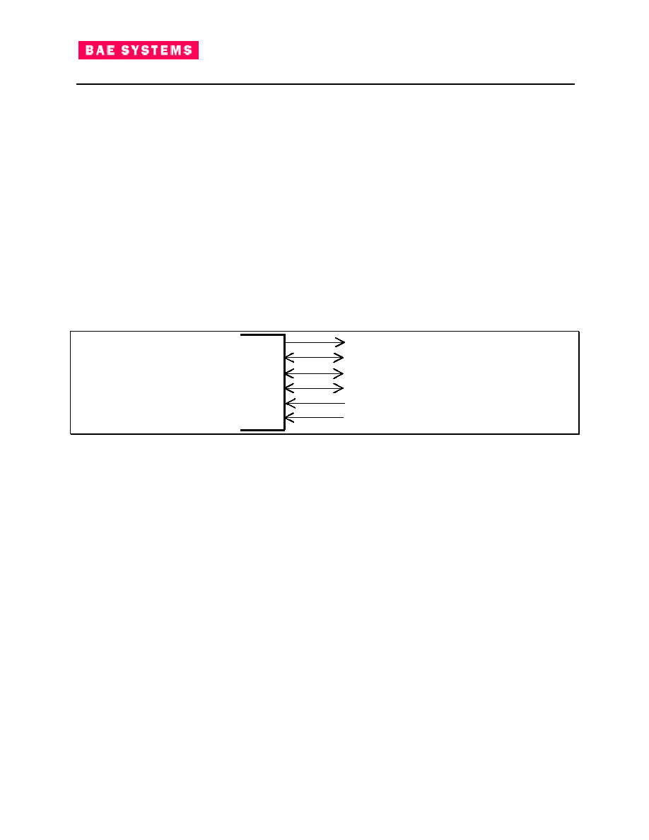
67
Document #: 234A533
RAD750 3U CompactPCI
Hardware Users Manual
If JTS_PROBE_PRESENT_L is high and either the Master En bit of the JTAG Control/Status Port A
register in the Power PCI ASIC is low or the JTB_MSTR_EN_IN input is low, the port responds solely as
a JTAG slave to an external backpanel master.
If JTS_PROBE_PRESENT_L is low and either the Master En bit of the JTAG Control/Status Port A
register in the Power PCI ASIC is low or the JTB_MSTR_EN_IN input is low, this port will not respond to
any external backpanel master or control any external backpanel slave.
If JTS_PROBE_PRESENT_L is low and both the Master En bit of the JTAG Control/Status Port A
register in the Power PCI ASIC is high and the JTB_MSTR_EN_IN input is high, this port will control the
external backpanel JTAG interface through the JTAG Control/Status Port A registers but not include the
Power PCI ASIC slave JTAG port in this JTAG string.
If JTS_PROBE_PRESENT_L is high and both the Master En bit of the JTAG Control/Status Port A
register in the Power PCI ASIC is high and the JTB_MSTR_EN_IN input is high, this port will control the
external backpanel JTAG interface through the JTAG Control/Status Port A registers and include the
Power PCI ASIC slave JTAG port in this JTAG string.
This port uses the set of signals listed below as described in the JTAG IEEE 1149.1a Standard. Figure
17 shows the signals that make up this interface.
JTAG
Backpanel
Interface
JTMS_TCLK
JTMS_TMS
JTMS_TDI
JTMS_TRST_
L
JTMS_TDO
JTMS_MSTR_EN_IN
Figure 17: JTAG Backpanel Interface I/O
5.2.1.1.1 JTMS_TMS
JTAG Test Mode Select is used to control the state of the Test Access Port (TAP) in devices connected to
the backpanel JTAG interface. This signal is tied to the JTM_A_TMS(0) pin of the Power PCI ASIC.
When the RAD750 3U CompactPCI board is controlling this JTAG interface, JTMS_TMS is an output.
When the RAD750 3U CompactPCI board is responding solely as a JTAG slave, it is an input.
Otherwise, this signal is tri-stated.
This signal is tied to an 8.2K Ohm pull-up resistor.
5.2.1.1.2 JTMS_TCLK
JTAG Test Clock is used to clock state information and test data into and out of the devices connected to
the backpanel JTAG interface during TAP operation.
When the RAD750 3U CompactPCI board is controlling this JTAG interface, JTMS_TCLK is an output.
When the RAD750 3U CompactPCI board is responding solely as a JTAG slave, it is an input.
Otherwise, this signal is tri-stated.
This signal is tied to an 8.2K Ohm pull-up resistor.

68
Document #: 234A533
RAD750 3U CompactPCI
Hardware Users Manual
5.2.1.1.3 JTMS_TDO
JTAG Test Data Out is used to serially shift test data and test instructions into devices connected to the
backpanel JTAG interface in a string during TAP operations.
When the RAD750 3U CompactPCI board is controlling this JTAG interface, JTMS_TDO is an output
from the JTAG Master Port A in the Power PCI ASIC. When the RAD750 3U CompactPCI board is
responding solely as a JTAG slave, it is an output from the JTAG Slave Port in the Power PCI ASIC.
Otherwise, this signal is tri-stated.
5.2.1.1.4 JTMS_TRST_L
JTAG Test Reset is driven active to initialize the TAP controllers in devices connected to the backpanel
JTAG interface.
When the RAD750 3U CompactPCI board is controlling this JTAG interface, JTMS_TRST_L is an output.
When the RAD750 3U CompactPCI board is responding solely as a JTAG slave, it is an input.
Otherwise, this signal is tri-stated.
This signal is tied to a 1K Ohm pull-down resistor.
5.2.1.1.5 JTMS_TDI
The RAD750 3U CompactPCI board receives serially shifted test data from other devices on the
backpanel JTAG interface via the JTAG Test Data In during TAP operations. This signal is always an
input.
When the RAD750 3U CompactPCI board is controlling this JTAG interface, JTMS_TDI is an input to
either JTAG Master Port A or the JTAG slave port in the Power PCI ASIC depending on whether the
slave port is included in the JTAG string. When the RAD750 3U CompactPCI board is responding solely
as a JTAG slave, it is an input to the JTAG Slave Port in the Power PCI ASIC.
This signal is tied to an 8.2K Ohm pull-up resistor.
5.2.1.1.6 JTMS_MSTR_EN_IN
The JTAG Backpanel Interface Master Enable signal controls whether the JTAG backpanel interface may
be controlled by this RAD750 3U CompactPCI board. When low, all primary non-data outputs are tri-
stated and used solely as inputs.
Typically, this signal is allowed to float high for a card in the system slot and tied low for a card in a
peripheral slot. For fault tolerance reasons, multiple cards may be configured as possible masters and
multiple positions may be floated high relying on the internal Master En bit of the JTAG Control/Status
Port A register in each Power PCI ASIC to enable the appropriate slot as master of the JTAG interface.
This signal is tied to an 8.2K Ohm pull-up resistor.
5.2.1.2 RAD750 JTAG (COP) Interface
The RAD750 JTAG (COP) Interface primarily functions as a slave JTAG interface port on the RAD750 to
an external processor emulator probe for hardware / software debug. When this interface is not
connected to such a probe, the RAD750 port allows internal RAD750 3U CompactPCI board access
through the Power PCI ASIC JTAG Master Port B.
If either the Master En bit of the JTAG Control/Status Port B register in the Power PCI ASIC is low or
the JT7_MSTR_EN_IN input is low, the RAD750 port will respond solely as a JTAG slave to an external
probe.
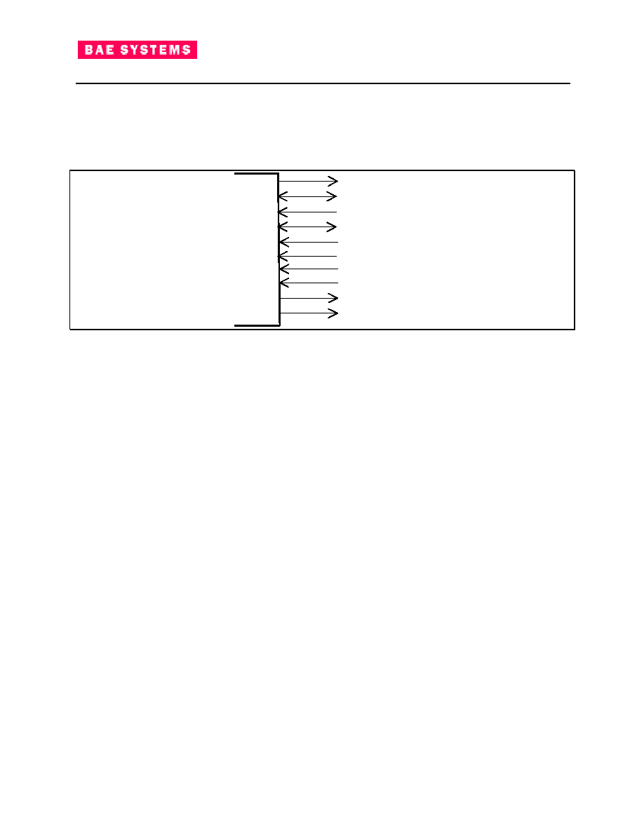
69
Document #: 234A533
RAD750 3U CompactPCI
Hardware Users Manual
If both the Master En bit of the JTAG Control/Status Port B register in the Power PCI ASIC is high and
the JT7_MSTR_EN_IN input is high, the RAD750 port will be controlled through the JTAG
Control/Status Port B registers in the Power PCI ASIC and must not be controlled externally.
This port supports the set of signals listed below as described in the JTAG IEEE 1149.1a Standard.
Figure 18 shows the signals that make up this interface.
JTAG
RAD750
Interface
JTM_TCLK
JTM_TMS
JTM_TDI
JTM_TRST_L
JTM_TDO
JTM_MSTR_EN_IN
JTM_RESET_L
JTM_SRESET_L
CPU_CHKSTP_L
JTM_POWER
Figure 18: JTAG RAD750 Interface I/O
5.2.1.2.1 JTM_TMS
JTAG Test Mode Select is used to control the state of the Test Access Port (TAP) in the RAD750. This
signal is tied to the JTM_B_TMS(0) pin of the Power PCI ASIC.
When the RAD750 3U CompactPCI board is controlling this JTAG interface, JTM_TMS is an output.
When the RAD750 3U CompactPCI board is responding solely as a JTAG slave, it is an input.
Otherwise, this signal is tri-stated.
5.2.1.2.2 JTM_TCLK
JTAG Test Clock is used to clock state information and test data into and out of the RAD750 during TAP
operation.
When the RAD750 3U CompactPCI board is controlling this JTAG interface, JTM_TCLK is an output.
When the RAD750 3U CompactPCI board is responding solely as a JTAG slave, it is an input.
Otherwise, this signal is tri-stated.
5.2.1.2.3 JTM_TDO
JTAG Test Data Out is used to serially shift test data and test instructions into the RAD750 during TAP
operations. This signal is always an output from the RAD750 during JTAG operations. Otherwise, this
signal is tri-stated.
5.2.1.2.4 JTM_TRST_L
JTAG Test Reset is driven active to initialize the TAP controller in the RAD750. This signal is always an
input.
5.2.1.2.5 JTM_TDI
The RAD750 receives serially shifted test data from either the external emulator probe or the internal
Power PCI ASIC during TAP operations. This signal is always an input.
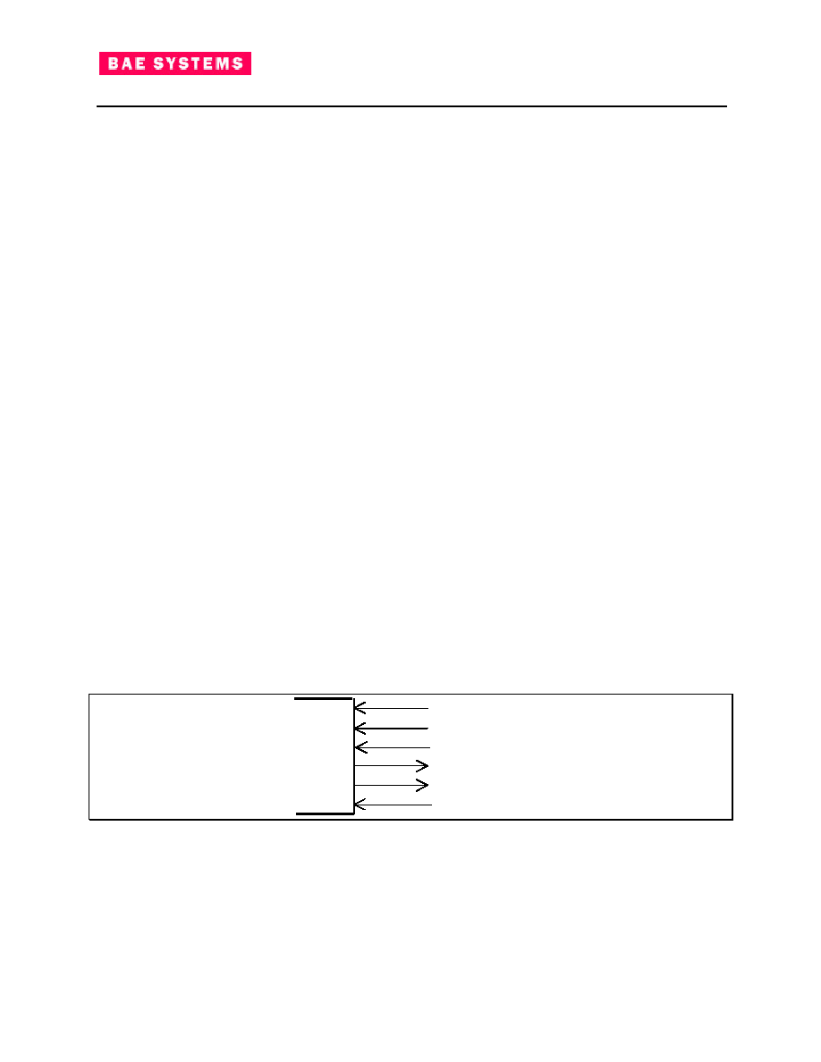
70
Document #: 234A533
RAD750 3U CompactPCI
Hardware Users Manual
5.2.1.2.6 JTM_MSTR_EN_IN
The RAD750 JTAG Interface Master Enable signal controls whether the RAD750 JTAG slave port may be
controlled by this RAD750 3U CompactPCI board. When low, all primary non-data outputs are tri-stated
and used solely as inputs.
This signal should be tied low when an emulator probe is attached to the RAD750 3U CompactPCI board
to prevent any chance of both the probe and Power PCI ASIC trying to control this port at the same time.
However, if this is impossible, then software must solely control this through the internal Master En bit of
the JTAG Control/Status Port B register in the Power PCI ASIC.
5.2.1.2.7 JTM_SRESET_L
This signal causes a soft reset of the RAD750.
5.2.1.2.8 JTM_RESET_L
This signal causes a hard reset to the RAD750 3U CompactPCI board. It shall have the same effect as
MISC_POR_L.
5.2.1.2.9 CPU_CKSTP_L
This signal, when low indicates the RAD750 has detected a Checkstop condition and is entering
checkstop mode where it is gating off all clocks and tri-stating all outputs. When high, this signal
indicates the RAD750 is running normally.
5.2.1.2.10 JTM_POWER
This signal provides a sensing output of the 3.3V power of the RAD750 3U CompactPCI board. 3.3V is
connected to this pin through a 1K Ohm series resistor.
5.2.1.3 Power PCI JTAG Slave Interface
The Power PCI JTAG slave interface supports the control of the Power PCI ASIC JTAG slave port
through an external JTAG connection. If JTS_PROBE_PRESENT_L is tied low, the external signals are
connected to the Power PCI ASIC JTAG slave port. Otherwise, the slave port is connected to the
Backpanel JTAG Interface string. The set of signals listed below as described in the JTAG 1149.1a
Standard. All signals must be synchronous to the JTS_TCLK except JTS_TRST_L. Figure 19 shows all
the signals in this interface.
JTAG
Power
PCI
Interface
JTS_TCLK
JTS_TDO
JTS_TRST_L
JTS_PRO_PRE_L
JTS_TDI
JTS_TMS
Figure 19: JTAG Slave Interface I/O
5.2.1.3.1 JTS_TMS
JTAG Test Mode Select is used to control the state of the Test Access Port (TAP) in the Power PCI ASIC
JTAG Slave Core.
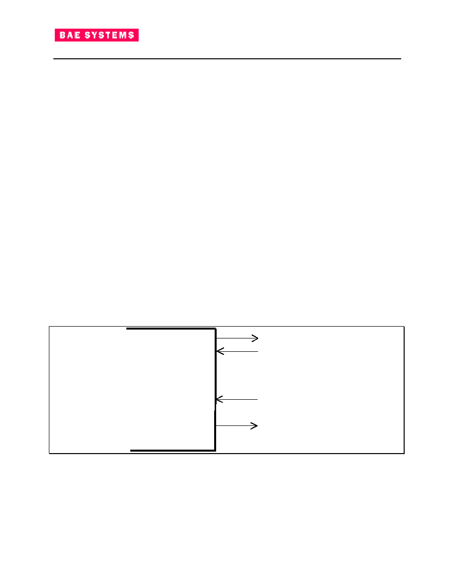
71
Document #: 234A533
RAD750 3U CompactPCI
Hardware Users Manual
5.2.1.3.2 JTS_TCLK
JTAG Test Clock is used to clock state information and test data into and out of the Power PCI ASIC
JTAG Slave Core during TAP operation.
5.2.1.3.3 JTS_TDI
JTAG Test Data In is used to serially receive test data and test instructions from the JTAG Master during
TAP operations.
5.2.1.3.4 JTS_TDO
JTAG Test Data Out is used to serially shift test data and test instructions into the external probe
connected to JTAG in a string during TAP operations.
5.2.1.3.5 JTS_TRST_L
When JTAG Test Reset is driven active, the TAP controller in the Power PCI JTAG core shall be
initialized.
5.2.2 UART Interface
The UART interface on the RAD750 3U CompactPCI board sends and receives signals external to the
chip. These signals include the serial data and MODEM control signals.
The RAD750 3U CompactPCI board uses no separate transceivers for this interface. Users must convert
this to RS-232 or RS-422 external to the RAD750 3U CompactPCI board.
Because this is the primary software debug interface for the RAD750 3U CompactPCI board, these
signals are routed to both a set of user backpanel signals (J2) and the front panel connector (J7). Users
must connect to no more than one of these two interfaces at a time. A picture of this Interface and its
signals is shown in Figure 20.
UART
Interface
UART_TX_DATA
UART_RX_DATA
UART_CTS_L
UART_RTS_L
Figure 20: Peripheral Device Interface I/O
5.2.2.1 UART_TX_DATA
This signal is the serial data output to the communications link. This value is driven to a 0b`1' on reset.

72
Document #: 234A533
RAD750 3U CompactPCI
Hardware Users Manual
5.2.2.2 UART_RX_DATA
This port is the serial data input from the communications link.
5.2.2.3 UART_CTS_L
Clear to Send is an active low signal that indicates the MODEM or data set is ready to exchange data.
The compliment of this signal is stored in bit 4 of the MODEM Status Register. Bit 0 of the MODEM
Status Register indicates whether this signal has changed since the last time the MODEM Status
Register was read. Whenever bit 4 of the MODEM Status Register changes state an interrupt is sent if
the MODEM Status interrupt is enabled.
5.2.2.4 UART_RTS_L
Request to Send is an active low output signal that informs the MODEM or data set that the UART is
ready to exchange data. Bit 1 of the MODEM Control Register controls the output of this signal. A reset
sets this signal to an inactive (high) state.
5.2.3 Interrupts and Discretes
The RAD750 3U CompactPCI board provides the following interrupts and discretes on the main
backpanel connectors (J1 and J2).
5.2.3.1 MISC _PID(31:0)
The 32 Programmable Interrupt/Discrete lines are individually configurable via software to be enabled as
inputs or outputs or to be disabled. The RAD750 3U CompactPCI board allows software to use PIDs
configured as inputs to provide controls for the internal chip timers, discrete inputs, and interrupts (both
vector interrupts to be handled by the internal EMC and normal interrupts handled by the embedded
interrupt controller).
Table 16 shows the configurations for each pin that is supported by the RAD750 3U CompactPCI board.
As an input, when a PID is configured to set the PID Input Register in the Power PCI ASIC, it can be
configured so that the PID In Register bit will be set to a one either when a level of 1 is seen on the pin or
on a falling edge transition. The values in the PID In Register can also be configured via software to
generate interrupts or to be simply used as discretes.
MISC_PID16 is connected on the RAD750 3U CompactPCI board to PCI_INTA#. This must be
configured as an input only because PCI requires that any output be open drain. It may be configured as
interrupt input if this is the Resource Controller slot. It may be configured as an output only if the system
is not implementing PCI interrupts. See Section 5.2.3.5 for more details on PCI_INTA#.
MISC_PID17 is connected on the RAD750 3U CompactPCI board to PCI_INTB#. This must be
configured as an input only because PCI requires that any output be open drain. It may be configured as
interrupt input if this is the Resource Controller slot. It may be configured as an output only if the system
is not implementing PCI interrupts. See Section 0 for more details on PCI_INTB#.
MISC_PID18 is connected on the RAD750 3U CompactPCI board to PCI_DEG#. This must be
configured as an input only because PCI requires that this be sourced by a power supply. It may be
configured as interrupt input in any slot position. It may be configured as an output only if the system is
not implementing this power signal.
MISC_PID19 is connected on the RAD750 3U CompactPCI board to PCI_FAL#. This must be configured
as an input only because PCI requires that this be sourced by a power supply. It may be configured as
interrupt input in any slot position. It may be configured as an output only if the system is not
implementing this power signal.

73
Document #: 234A533
RAD750 3U CompactPCI
Hardware Users Manual
MISC_PID20 is connected on the RAD750 3U CompactPCI board to PCI_ENUM#. This must be
configured as an input only because PCI requires that any output be open drain. It may be configured as
interrupt input if this is the Resource Controller slot.
MISC_PID28 is connected on the RAD750 3U CompactPCI board to PCI_INTC#. This must be
configured as an input only because PCI requires that any output be open drain. It may be configured as
interrupt input if this is the Resource Controller slot. It may be configured as an output only if the system
is not implementing PCI interrupts. This can be used as interrupt to the RAD750 or a vector interrupt to
the EMC in the Power PCI ASIC. See Section 5.2.3.7 for more details on PCI_INTC#.
MISC_PID29 is connected on the RAD750 3U CompactPCI board to PCI_INTD#. This must be
configured as an input only because PCI requires that any output be open drain. It may be configured as
interrupt input if this is the Resource Controller slot. It may be configured as an output only if the system
is not implementing PCI interrupts. This can be used as interrupt to the RAD750 or a vector interrupt to
the EMC in the Power PCI ASIC. See Section 5.2.3.8 for more details on PCI_INTD#.
Table 16 - PID Definition Table
Signal Name
PID Input
Function
Power PCI Input
Function
PID Output
Function
Power PCI
ASIC
Output
Function
External
Function
MISC_PID31
PID In Reg 31
Vector Interrupt 5
PID Out Reg 31
MISC_PID30
PID In Reg 30
Vector Interrupt 4
PID Out Reg 30
MISC_PID29
PID In Reg 29
Vector Interrupt 3
PID Out Reg 29*
PCI_INTD#
MISC_PID28
PID In Reg 28
Vector Interrupt 2
PID Out Reg 28*
PCI_INTC#
MISC_PID27
PID In Reg 27
Vector Interrupt 1
PID Out Reg 27
MISC_PID26
PID In Reg 26
Vector Interrupt 0
PID Out Reg 26
MISC_PID25
PID In Reg 25
PID Out Reg 25
MISC_PID24
PID In Reg 24
PID Out Reg 24
MISC_PID23
PID In Reg 23
PID Out Reg 23
MISC_PID22
PID In Reg 22
PID Out Reg 22
MISC_PID21
PID In Reg 21
PID Out Reg 21
MISC_PID20
PID In Reg 20
PID Out Reg
20***
PCI_ENUM#
MISC_PID19
PID In Reg 19
PID Out Reg 19**
PCI_FAL#
MISC_PID18
PID In Reg 18
PID Out Reg 18**
PCI_DEG#
MISC_PID17
PID In Reg 17
PID Out Reg 17*
PCI_INTB#
MISC_PID16
PID In Reg 16
PID Out Reg 16*
PCI_INTA#
MISC_PID15
PID In Reg 15
PID Out Reg 15
MISC_PID14
PID In Reg 14
PID Out Reg 14
MISC_PID13
PID In Reg 13
PTIM3 Clear
PID Out Reg 13
MISC_PID12
PID In Reg 12
PTIM3 Snapshot
PID Out Reg 12
MISC_PID11
PID In Reg 11
PTIM3 Clock
PID Out Reg 11
MISC_PID10
PID In Reg 10
PTIM2 Clear
PID Out Reg 10
MISC_PID09
PID In Reg 09
PTIM2 Snapshot
PID Out Reg 09
MISC_PID08
PID In Reg 08
PTIM2 Clock
PID Out Reg 08
MISC_PID07
PID In Reg 07
PTIM1 Clear
PID Out Reg 07
MISC_PID06
PID In Reg 06
PTIM1 Snapshot
PID Out Reg 06

74
Document #: 234A533
RAD750 3U CompactPCI
Hardware Users Manual
Signal Name
PID Input
Function
Power PCI Input
Function
PID Output
Function
Power PCI
ASIC
Output
Function
External
Function
MISC_PID05
PID In Reg 05
PTIM 1 Clock
PID Out Reg 05
MISC_PID04
PID In Reg 04
PID Out Reg 04
WD Timer
Heartbeat
MISC_PID03
PID In Reg 03
PID Out Reg 03
WD Timer
Expired
MISC_PID02
PID In Reg 02
PID Out Reg 02
PTIM 3
Output
MISC_PID01
PID In Reg 01
PID Out Reg 01
PTIM 2
Output
MISC_PID00
PID In Reg 00
PID Out Reg 00
PTIM 1
Output
* PID may be output only if PCI interrupts not implemented in system.
** PID may be output only if CompactPCI power signals not implemented in system.
***PID may never be output.
5.2.3.2 UART_IO_OUT1_L
This programmable output signal will be an active low signal that is user-designated. Bit 2 of the MODEM
Control Register in the Power PCI ASIC controls the output of this signal. This signal resets to its
inactive high state.
5.2.3.3 UART_IO_OUT2_L
This programmable output signal will be an active low output signal. Bit 3 of the MODEM Control
Register of the Power PCI ASIC controls the output of this signal. This signal resets to its inactive high
state. This signal is connected on the RAD750 3U CompactPCI board to PCI_INTA# in order to provide
an open drain driver for this signal on cards needing to generate a PCI interrupt.
5.2.3.4 MISC_NMI_L
The non-maskable interrupt input causes a machine check interrupt to be posted to the RAD750. This
signal shall be NOR'd through logic with any non-maskable interrupt conditions in the Power PCI ASIC to
generate the Machine Check Interrupt (MCP) to the RAD750.
5.2.3.5 PCI_INTA#
This active low interrupt signal causes an interrupt to be seen by RAD750 when the RAD750 3U
CompactPCI board is configured to process interrupts on this pin. Externally generated interrupts must
conform to the requirements in the PCI Specification.
The RAD750 3U CompactPCI board can be configured to generate a single function PCI interrupt on this
pin using the Open Drain output from UART_OUT2_L. This would typically be used when the RAD750
3U CompactPCI board is not the Resource Controller for its processor subsystem.
5.2.3.6 PCI_INTB#
This active low interrupt signal causes an interrupt to be seen by RAD750 when the RAD750 3U
CompactPCI board is configured to process interrupts on this pin. Externally generated interrupts must

75
Document #: 234A533
RAD750 3U CompactPCI
Hardware Users Manual
conform to the requirements in the PCI Specification. The RAD750 3U CompactPCI board should not be
configured to generate an output on this pin unless no card in the subsystem supports PCI Interrupts.
5.2.3.7 PCI_INTC#
This active low interrupt signal causes an interrupt to be seen by RAD750 when the RAD750 3U
CompactPCI board is configured to process interrupts on this pin. Externally generated interrupts must
conform to the requirements in the PCI Specification. The RAD750 3U CompactPCI board should not be
configured to generate an output on this pin unless no card in the subsystem supports PCI Interrupts.
5.2.3.8 PCI_INTD#
This active low interrupt signal causes an interrupt to be seen by RAD750 when the RAD750 3U
CompactPCI board is configured to process interrupts on this pin. Externally generated interrupts must
conform to the requirements in the PCI Specification. The RAD750 3U CompactPCI board should not be
configured to generate an output on this pin unless no card in the subsystem supports PCI Interrupts.
5.2.4 Resets and Clocks
The RAD750 3U CompactPCI board provides the following general reset and clock signals.
5.2.4.1 MISC_POR_L
The RAD750 3U CompactPCI board receives and processes the MISC_POR_L as an asynchronous
reset for the entire board. This signal causes the Power PCI ASIC and RAD750 to be changed to their
default states. It also causes all signals to be placed in their Reset states.
5.2.4.2 CLK_EXT_SYS_OSC
When CLK_EXT_SYS_OSC_SEL_L is active, this signal is used by the RAD750 3U CompactPCI board
as an alternate clock signal (instead of the onboard oscillator) from which all other internally generated
system, PCI, real-time, and JTAG clock signals are generated. It must have a maximum frequency of 33
MHz with no minimum frequency. The duty cycle of this signal must be between 40% (
TBR
) and 60%
(
TBR
).
5.2.4.3 CLK_EXT_SYS_OSC_SEL_L
This signal is used to select whether the RAD750 3U CompactPCI board should use the onboard
oscillator or the input CLK_EXT_SYS_OSC as an the clock signal from which all other internally
generated system, PCI, real-time, and JTAG clock signals are generated.
This signal shall be tied to an 8.2K Ohm pull-up resistor.
5.2.5 Configuration Inputs
The RAD750 3U CompactPCI board provides the following configuration input signals.
5.2.5.1 PCI_GA(4:0,P)
The PCI Geographical Address bits are provided for boards that require a unique slot address for each
board in a subsystem. These pins are unused on the RAD750 3U CompactPCI board.
5.2.5.2 I2C(1:0)
The I
2
C interface is used as a configuration and status interface in some systems. These pins are
unused on the RAD750 3U CompactPCI board.

76
Document #: 234A533
RAD750 3U CompactPCI
Hardware Users Manual
5.2.5.3 MISC_ROM_ON_PCI
This active high signal indicates that there is ROM in the upper 16 MB of the PCI Memory Address space.
When this signal is high, the RAD750 3U CompactPCI board maps memory accesses in the upper 8 or
16 MB (depending on Power PCI ASIC memory control registers) from the RAD750 to PCI Memory bus.
Otherwise, such accesses are mapped to on-card EEPROM or treated as non-existent memory.
This signal is tied to an 8.2K Ohm pull-up resistor.
5.2.5.4 CHASSIS_GRND(0:1)
These pins are attached to 5 M Ohm resistors to ground on the RAD750 3U CompactPCI board. They
may be utilized for chassis to signal isolation verification and redundant chassis grounding.
5.3 Power Interfaces
The RAD750 3U CompactPCI board operates on a single 3.3V supply connected through the main
connector (J1).
At least one 0.1
µ
F ceramic capacitor suitable for high speed decoupling is provided for the +3.3V voltage
close to the connector to decouple every 10 power pins.
At least one 10
µ
F tantalum capacitor is located close to the connector and 3.3V pins.
The RAD750 3U CompactPCI board does not utilize power from the +5V, -12V or +12V inputs on the
main connector (J1).
Other than required pull-ups, the RAD750 3U CompactPCI board does not utilize the V(I/O) pins on the
main connector (J2).
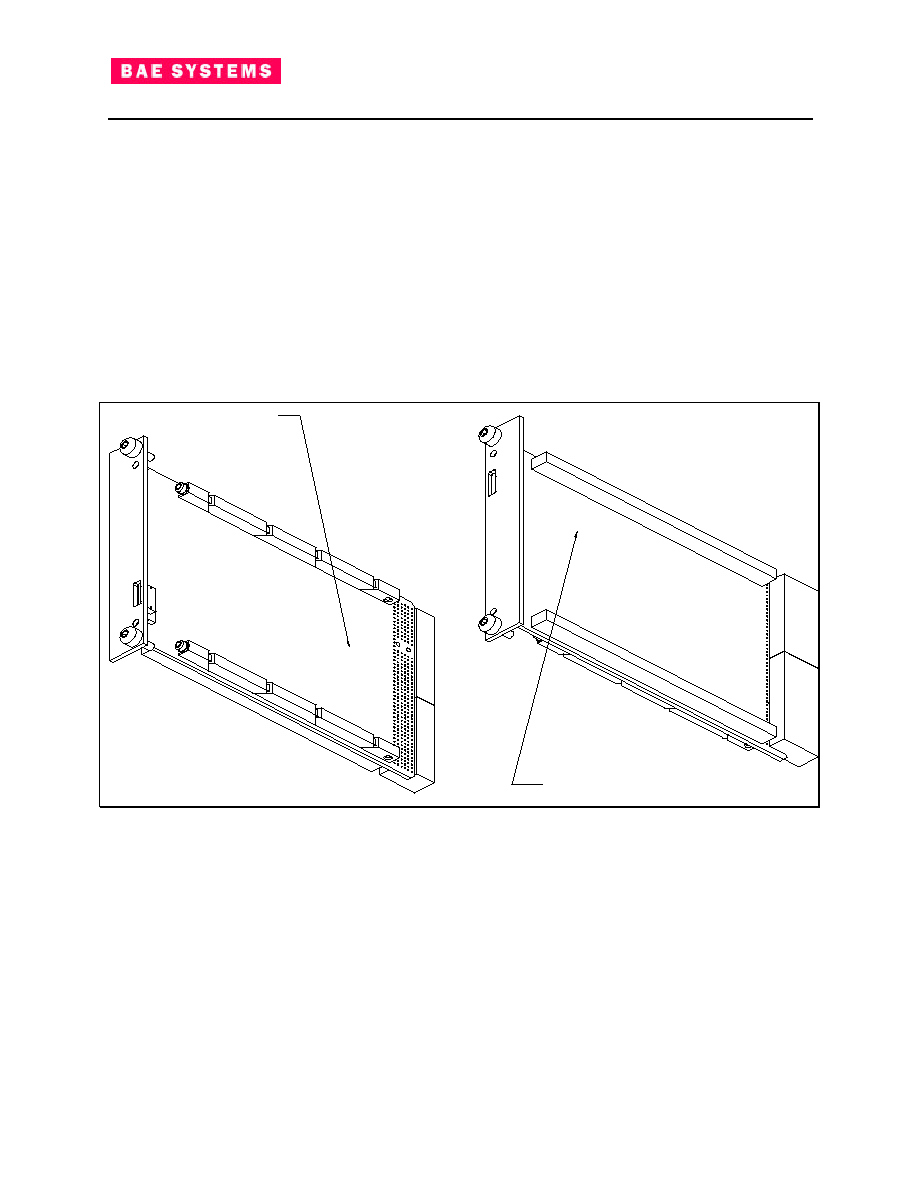
77
Document #: 234A533
RAD750 3U CompactPCI
Hardware Users Manual
6 Hardware / Mechanical
The RAD750 board mechanical characteristics are based on the CompactPCI RAD750 3U board
standard. The board format is double sided, conduction cooled, based on the IEEE-1101.1 Conduction
Cooled board format. Figure 21 is a depiction of the basic board layout. The top of the board is shown
on the right hand side (i.e., with the stiffeners), and the bottom of the board is shown on the left (i.e., with
the multi-segment wedgelocks). A 25-pin connector that provides access to the UART and JTAG signals
from the Power PCI and RAD750 is provided on the front panel. These same signals are also available
on the CompactPCI connector. The front panel is complaint with IEEE 1101.10. The board fits in a
standard CompactPCI backplane and maintains the standard overall pitch restriction of 0.8 inches. The
board does not use a frame. The RAD750 board is constructed with PCB trace characteristic impedance
of 65
±
10 ohms. The RAD750 board does not connect chassis ground through a low impedance path to
logic ground used on the board. The RAD750 board provides a single ejector/injector handle compliant
with IEEE 1101.10 for insertion and removal. The RAD750 board is conformal coated. The RAD750
board mass is approximately 0.5 Kg not including shielding.
Max Allowable Component
Height 6.0MM [0.236 IN]
Max Allowable Component
Height 10.0MM [0.393 IN]
Figure 21: Isometric View of the RAD750 Board Layout
Figure 22 is flat view of the boards and provides more dimensional information about the board.
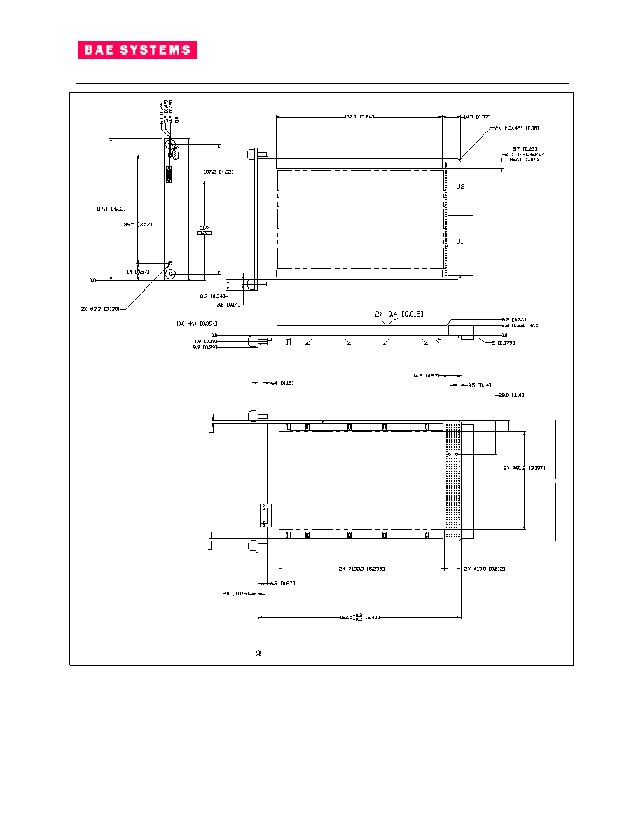
78
Document #: 234A533
RAD750 3U CompactPCI
Hardware Users Manual
*Components and Associated
Circuitry within this area
Both Sides
*Components and Associated
Circuitry within this area
Both Sides
Figure 22: Standard View of the RAD750 Board Layout
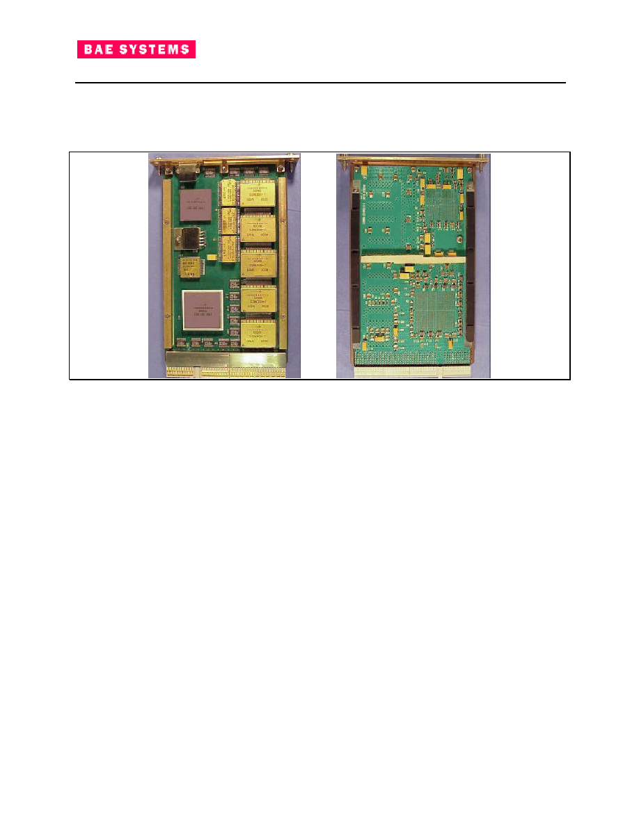
79
Document #: 234A533
RAD750 3U CompactPCI
Hardware Users Manual
6.1 Location Overview
Figure 23 highlights the position of the important RAD750 board components. Depending on the board
type it might be that your board does not include all components named in the location diagram.
Figure 23: RAD750 Board Layout
6.2 Grounding
6.2.1 Structural Grounding
Preparation of metal-to-metal surfaces for electrical bonding purposes is made in accordance with
MIL-B-5087B, paragraph 3.1.4.
6.2.2 Circuit Grounding, General
Generally, all RAD750 board electronic interface circuitry is referenced to the System Reference Plane
with the lowest practicable impedance.
All circuitry interconnecting integrated circuits, semiconductors, discrete devices, transformers, and other
electronic components is provided with an electrical path to structure, at all times. This reference point is
called the Circuit Common. The single point grounding method must be used for all Circuit Commons.
The Circuit Common must have a low resistance, low inductance path to structure (the System Reference
Plane).
Comment: The maximum required ground path resistance ranges from milliohms for low level electronic
circuits, to kilo-ohms for circuits with current-limiting resistance for fault conditions, to megohms for
circuits only requiring electrostatic discharge paths. The single point grounding method requires that
there be no more than one path from any circuit or group of circuits to structure but does not require the
use of only one ground tree.

80
Document #: 234A533
RAD750 3U CompactPCI
Hardware Users Manual
6.2.3 Wire Shield Grounding
RAD750 board High speed data bus interfaces use a grounded metallic backshell as the means of
terminating each end of a cable shield to chassis at each connector.
6.2.4 ESD Grounding
All metallic elements, including wires, unused conductors of cable, connectors, circuit board traces, spot
shields, and other conductive elements greater than 3 cm
2
in surface area or longer than 25 cm, have a
conductive path to structure with a resistance <1E8 ohms when measured in air or <1E12 ohms when
measured in vacuum.

81
Document #: 234A533
RAD750 3U CompactPCI
Hardware Users Manual
7 Manufacturing
7.1 Organic Materials
The Organic/non-metallic materials listed in Table 17 will be utilized in manufacturing the RAD750 3U
CompactPCI board. Use the following descriptions to interpret the data in each of the columns.
Material
Material Description
Specifications
All materials specifications that are used for purchasing and manufacture
Vendor
Source of material
TVS
Thermal Vacuum Stability properties, as tested per ASTM-E595
Flammability per NHB 8060.1B;
A
Meets Test 1, NHB 8060.1 requirement in the thickness and test condition
specified.
B
Material, in thickness specified, failed Test 1, NHB 8060.1 in the specified test
atmosphere with a burn length of more than 6 inches but less than 12 inches.
C
Material, in thickness specified, burned totally in Test 1 with flame propagation
rate of less than 0.1 in Test 2.
U
Untested
X
Fails criteria of Test 1. Fails to meet criteria for above ratings or has moderate to
heavy burn dripping.
S
Special test, see explanation.
FLA
I
Insufficient data
Toxic offgassed substances per NHM 8060.1B
K
Meets MAC (100 lbs.) values without special cure
A
Meets MAC (10 lbs. max.) values without special cure
B
Meets MAC (100 lbs. or 10 lbs. max.); listed in NHB 8060.1 for the quantities
given.
U
Untested
V
Meets MAC (5 lbs. max.) values
X
Meets MAC values greater than that specified in NHB 8060.1 for the quantities
given.
S
Special test, see explanation.
TOX
I
Insufficient data
Amount used by:
-Total Weight, grams (TTL)
Amount
- Thickness, centimeters (THK)

82
Document #: 234A533
RAD750 3U CompactPCI
Hardware Users Manual
- Surface Area, square centimeters (SA)
- * designates that all material will be encapsulated by conformal coating
Application/Use
Application of material
Table 17 - Organic Materials
Material
Specifications
Vendor TVS
FLA TOX Amount
Application/Use
Uralane
5750
MIL-I-46058
6032466-1
Ciba
.65% TML
.01% CVCM
C
X
2.2 g TTL
.003 in. THK
46.62 in
2
SA
Conformal Coating for
PWAs
Uralane
5753
6032466-2
Ciba
.80% TML
.02% CVCM
C
B
10 g TTL*
.01 in. THK*
4 in
2
SA*
Component thermal
bonding Material
Laminate,
Polyimide,
GI,
Preimpreg
nated
MIL-S-13949/13
MIL-PRF-55110
161A671
Norplex .93% TML
.01% CVCM
S
S
TBD
g TTL*
TBD
in.
THK*
1.9 in
2
SA*
PWB Prepreg Material;
Amounts given include
OM003 & OM004
Laminate,
Copper-
Clad, G-I
Polyimide
MIL-S-13949/10
MIL-PRF-55110
Norplex .93% TML
.01% CVCM
S
S
PWB Core Material
Probimer
PR52M
Solder
Mask
IPC-SM-840,
Class 3
6032991
Ciba
.73% TML
.07% CVCM
S
S
1.7 g TTL*
.002 in.
THK*
46.6 in
2
SA*
PWB Solder Mask
Material
Epoxy
240A
IPC-SM-840,
Class 3
6032991
Hysol-
Dexter
.33% TML
.05% CVCM
S
S
Undetermine
d
PWB Solder Mask
Material; Will be used
for touch-up (rework)
only
Kapton H,
Polyimide
Film
MIL-P-46112,
Type I
181A219-1
DuPont .77% TML
.02% CVCM
A
V
.30 g TTL
.001 in. THK
.005 in. THK
Lead Isolation Material,
Used in repair/ rework
only
M-O-N
Ink, Black
MIL-I-43553
174A235-1
Hysol-
Dexter
.50% TML
.01% CVCM
A
B
Negligible
Marking Ink
M-9-N Ink,
White
MIL-I-43553
174A235-2
Hysol-
Dexter
.51% TML
.04% CVCM
A
X
Negligible
Marking Ink
Cat-L-Ink,
50-700R,
Black
MIL-I-43553
174A235-3
Hysol-
Dexter
.74% TML
.01% CVCM
A
X
Negligible
Marking Ink
Cat-L-Ink,
50-100R,
White
MIL-I-43553
174A235-4
Hysol-
Dexter
.64% TML
.01% CVCM
U
B
Negligible
Marking Ink
Epoxipatc
6032846
Hysol-
.81% TML
C
B
Negligible
Bonding Material used
83
Document #: 234A533
RAD750 3U CompactPCI
Hardware Users Manual
Material
Specifications
Vendor TVS
FLA TOX Amount
Application/Use
h Kit 1C
Dexter
.02% CVCM
to stake cover
mounting screws
7.2 Inorganic Materials
The Inorganic/metallic materials listed in Table 18 will be utilized in manufacturing the RAD750 board.
Use the following descriptions to interpret the data in each of the columns.
Material
Material Description
Specifications
All materials specifications that are used for purchasing and manufacture
SCC
Stress Corrosion Cracking Susceptibility; OK indicates acceptable
Surface Treat
Surface Treatments or Processes Used to Prevent Corrosion
Application/Use
Application of material
Table 18 - Inorganic Materials
Material
Specifications SCC
Surface Treat
Application/Use
Aluminum
6061-T6
QQ-A-250/11
6009940
6009974
Ok
MIL-C-5541, Cl. 3
or MIL-A-8625, Ty.
III
Face Plate of Card Assembly
Solder, SN60
QQ-S-571
Ok
N/A, Conformal
Coated
Soldering on PWAs
Solder, SN62
QQ-S-571
Ok
N/A, Conformal
Coated
Soldering on PWAs
Solder, SN63
QQ-S-571
Ok
N/A, Conformal
Coated
Soldering on PWAs
Stainless Steel,
300 Series,
QQ-S-766
NAS620
Ok
QQ-P-35
Flat Washer
Stainless Steel,
300 Series, FF-
S-92
MS51957
Ok
ASTM A380
Pan Head Screw
7.3 Processes
The processes listed in Table 19 will be utilized in manufacturing the RAD750 board. Use the following
descriptions to interpret the data in each of the columns.
Process
Procedure Description
Specification
Specification number associated with the process
Materials
All materials affected by the process
Application/Use
Application of material
Table 19 - Processes

84
Document #: 234A533
RAD750 3U CompactPCI
Hardware Users Manual
Process
Specification
Materials
Application/Use
Printed Wiring, Flexible and
Rigid-flex
MIL-P-50884
All Flexible
PWBs
Manufacturing requirements for flex circuits
Printed Wiring Boards
MIL-PRF-
55110
IPC-6012
All Rigid
PWBs
Manufacturing requirements for rigid PWBs
Chemical Conversion
Coatings
MIL-C-5541,
Class 3
Aluminum
Surface treatment for Aluminum
Passivation Treatments for
Corrosion Resistant Steels
QQ-P-35
All CRESs
Cleaning/descaling procedure for CRESs
Standard Requirements for
Soldering
WS6006000
NHB5300.4
All Printed
Wiring
Assemblies
All soldering operations
Forming Flatpack leads
MA100-108
Flatpacks
Flatpack Forming tool procedure
ESD handling
MA100-161
ESD
grounding
Handling of ESD sensitive items
Continuity Checking Wires
MA100-163
Wires
Verifying Electrical Continuity after Attaching
Wires
Handling of removed
components for Failure
Analysis
MA100-206
Failed
Components
Handling of removed components for Failure
Analysis
Forming Quadpack Devices MA100-227
Forming
Dies
Quadpacks forming tool procedure
Handling Instruction of Card
Assy
MA100-228
Fragile
Leads
Handling Instruction of card Assy contains
components with fragile leads
Component / Material
Traceability
MA100-233
Component,
Material
Recording Component and Material
Traceability Data
Flux Removal
PP501-010
PWAs,
Solvent
Isopropanol
Cleaning of PWAs with IPA solvents
Flux Removal
PP501-011
PWAs,
Solvent EC-
7R
Cleaning of PWAs with BIOACT EC7-R
Part Marking Identification
PP502-004
Marking Inks Part Marking (only approved inks are used)
Bonding with Epoxy Patch
Kit
PP506-212
Epoxy Patch
Kit
Staking of screws
Application of Uralane
materials
PP508-202
Uralane
5753,
Uralane
5750,
components
, PWBs
Conformal coating with Uralane 5750, and
component thermal bonding with Uralane
5753
Tinning Electronic
Component Leads
PP509-224
Solder,
Component
Leads
Lead Tinning

85
Document #: 234A533
RAD750 3U CompactPCI
Hardware Users Manual
Process
Specification
Materials
Application/Use
Soldering Irons
PP509-220
Soldering
Irons
Soldering Iron selection, set-up and use
Component Removal
PP509-209
Solder
Gobbler or
Solder Wick
Component Removal using solder gobbler or
solder wick method
Hand Soldering
PP509-210
PWB
Hand soldering of components to PWB
PWB Surface Ionic Testing
PP511-003
Omega
Meter
PWB surface resistivity testing prior to
conformal coat
PWB Rework
PP515-014
Electrical
components
Procedure for the preparation, attachment,
and soldering of supplemental wires to
assemblies.
PWB Rework, Bushings
PP515-021
PWB
Procedure for installation of isolation
busings, machining holes, adding
components, and making internal conductor
interruptions.
Flatpack removal and
replacement
PP515-025
PWB,
Flatpacks
Procedure for removal and replacement of
flatpacks
Quadpack Soldering
PP516-002
PWB,
Quadpacks
Quadpack assembly and soldering
Assembly and Reword of
CGA
MA100-243
CGA
Assembly and rework of CGA component
X-ray Inspection
MA100-244
CGA
Real-time x-ray inspection of CGA solder
joints
7.4 Bill of Materials
The items listed in Table 20 will be utilized in manufacturing the RAD750 board.
Table 20 - Bill of Materials
Part Description
Part Number
Vendor
Quality
level
Package
Application/Use
1MB EEPROM
28LV010RPFS-20
SEI CORP.
SPACE
32 FP
Start-up Memory
SDRAM 64MB
STACK
233A634-1
BAE
SYSTEMS
SPACE
64 FP
Main Memory
OSCILLATOR, 33
MHz
MCM3040-2M
Q-TECH
CORP
SPACE
20 FP
Clock Source
REGULATOR
3.3V
233A633-1
OMNIREL
SPACE
TO-258AA
2.5V power for CPU
CPU RAD750
238A793
BAE
SYSTEMS
SPACE
360 CGA
Main Processor
Power PCI
238A791
BAE
SYSTEMS
SPACE
625 CGA
Bridge Chip
Cap. 0.01uF,
Ceramic
153A919-2
Kemet
SPACE
C0805
Bypass/Decoupling,
Cap. 0.1uF,
153A919-1
Kemet
SPACE
1210
Bypass/Decoupling

86
Document #: 234A533
RAD750 3U CompactPCI
Hardware Users Manual
Part Description
Part Number
Vendor
Quality
level
Package
Application/Use
Ceramic
Cap. 220pF,
CERAMIC
M123A10BPB221KS Kemet
0.001/1KH
C0805
Bypass/Decoupling
Cap. 10uF,
Tantalum
CWR09KC106KDB
AVX
/VISHAY
SPRAGUE
SPACE
CWR09
Bypass/Decoupling
Cap. 330uF,
Tantalum
223A635-2
AVX
SPACE
V
Bulk Storage
Res. 5M ohm
D55342K07B5T10S
SOI
0.001/1KHr RM1206
Pull-up/Down on
signals
Res. 100k ohm
D55342K07B100ES
SOI
0.001/1KHr RM1206
Pull-up/Down on
signals
R-Pack 10 ohm
234A801-1
Vishay/thin
Films
0.01%/1KH
r
24 P SSOP PCI Stub, Series
Termination, Isolated
resistors
R-Pack 1K ohm
234A801-5
Vishay/thin
Films
0.01%/1KH
r
16 P SSOP JTAG Pull-up & Pull-
Down Isolated
resistors
R-Pack 33.2 ohm
234A801-3
Vishay/thin
Films
0.01%/1KH
r
24 P SSOP Series Termination,
Isolated resistors.
R-Pack 8.2K ohm
234A801-8
Vishay/thin
Films
0.01%/1KH
r
24 P SSOP PCI Pull-Ups, N Res.
W/Common Pin
Ferrite Beads
HT50acb322513T
All American
N/A
Noise Control
Connectors - PCI
352152-1
AMP Corp.
SPACE
N/A
PCI back panel
connector
Connectors - PCI
352068-1
AMP Corp.
SPACE
N/A
PCI Back panel
connector
Front Panel
Connector 25 pin,
2 row
STM025SCDC012H
N
Nanonics
Corp.
SPACE
N/A
Test connector
Rail Key Green
Male
5-100525-4
N/A
Rail Key
Rail Key Green
Female
5-100526-4
N/A
Rail Key
Adapter Plate
TBD
N/A
Connector Adapter
Plate
Front Panel
10192430-1
JPL
Panel bracket,
front
234A513-1
(10192427-1)
JPL
N/A
Panel Bracket
Captive Jack
Screw
FT3003HS-6-2-2A
Fastener
Tech.
N/A
Secure the Card to
NHA
Wedge Lock
Screw
MS51957-3
87
Document #: 234A533
RAD750 3U CompactPCI
Hardware Users Manual
Part Description
Part Number
Vendor
Quality
level
Package
Application/Use
PCI Connector
Screw
MS51959-7
N/A
Card Lock
Retainer
265-1012-4.80 ET2L Calmark
N/A
Card Lock
Stiffener/Heat Sink 10192429-1
JPL
N/A
Card Stiffener

88
Document #: 234A533
RAD750 3U CompactPCI
Hardware Users Manual
8 Documentation
BAE SYSTEMS has reference documentation available for the RAD750 family of products. Visit the
RAD750 web site
http://www.rad750.com/
or contact your BAE SYSTEMS sales representative to obtain
copies.
∑
RAD750 Fact Sheet
∑
Power PCI Fact Sheet
∑
Power PCI Specification
∑
RAD750 Datasheet
∑
RAD750 Software Users Guide
∑
RAD750 Frequently Asked Questions (FAQ)
In addition to the documentation from BAE SYSTEMS, PowerPC documentation (i.e., Datasheets, User
Manuals, Application Notes, etc.) is also available from
IBM at
http://www.chips.ibm.com/products/powerpc/index.html
, and
Motorola at
http://www.mot.com/SPS/PowerPC/
.
8.1 Suggested Reading
This section lists additional reading that provides background for the information in this manual as well as
general information about the PowerPC architecture.
8.1.1 General PowerPC Information
The following documentation provides useful information about the PowerPC architecture and computer
architecture in general:
∑
The following book is available from the Morgan-Kaufmann Publishers, 340 Pine Street, Sixth
Floor, San Francisco, CA 94104; Tel. (800) 745-7323 (U.S.A.), (415) 392-2665 (International);
internet address:
mkp@mkp.com
.
1. -- The PowerPC Architecture: A Specification for a New Family of RISC Processors, Second
Edition, by International Business Machines, Inc.
Updates to the architecture specification are accessible via the world-wide web at
http://www.austin.ibm.com/tech/ppc-chg.html
.
∑
PowerPC Programming for Intel Programmers, by Kip McClanahan; IDG Books Worldwide, Inc.,
919 East Hillsdale Boulevard, Suite 400, Foster City, CA, 94404; Tel. (800) 434-3422 (U.S.A.),
(415) 655-3022 (International).
∑
PowerPC System Architecture, by Tom Shanley; Mindshare, Inc., 2202 Buttercup Drive,
Richardson, TX 75082; Tel. (214)231-2216 (U.S.A.), 021-706 6000 (United Kingdom), (800)420-
2677 (International).
8.1.2 IBM PowerPC Documentation
The PowerPC documentation is available from the links indicated above; the document order numbers
are included in parentheses for ease in ordering:
∑
Embedded Market Solutions - Publications: SC09-3032 - This is a CD-ROM containing
documentation on all the PowerPC family of products from IBM. The CD-ROM is updated
quarterly.
∑
Programming environments manuals - This book provides information about resources defined by
the PowerPC architecture that are common to PowerPC processors.
1. PowerPC Microprocessor Family: The Programming Environments G522-0290-00

89
Document #: 234A533
RAD750 3U CompactPCI
Hardware Users Manual
∑
Implementation Variances Relative to Rev. 1 of The Programming Environments Manual is
available via the world-wide web at
http://www.chips.ibm.com/
.
∑
Hardware specifications--Hardware specifications provide specific data regarding bus timing,
signal behavior, and AC, DC, and thermal characteristics, as well as other design considerations
for each PowerPC implementation. This include the following:
1. PowerPC 740
TM
and PowerPC 750
TM
Embedded RISC Microprocessor: Hardware
Specifications is available via the world-wide web at
http://www.chips.ibm.com/
.
2. PowerPC 750
TM
SCM RISC Microprocessor: Hardware Specification G522-0324-00
∑
Technical Summaries--Each PowerPC implementation has a technical summary that provides an
overview of its features. This document is roughly the equivalent to the overview (Chapter 1) of
an implementation's user's manual.
3. PowerPC 750 RISC Microprocessor Technical Summary is available via the world-wide web
at
http://www.chips.ibm.com/
.
1. PowerPC Microprocessor Family: 60x Bus Interface for 32-Bit Microprocessors, G522-0291-
00, provides a detailed functional description of the 60x bus interface, as implemented on the
601, 603, 604 and 740/750 family of PowerPC microprocessors. This document is intended
to help system and chipset developers by providing a centralized reference source to identify
the bus interface presented by the 60x family of PowerPC microprocessors.
∑
PowerPC Microprocessor Family: The Programmer's Reference Guide, MPRPPCPRG-01, is a
concise reference that includes the register summary, memory control model, exception vectors,
and the PowerPC instruction set.
∑
PowerPC Microprocessor Family: The Programmer's Pocket Reference Guide, SA14-2093-00
This foldout card provides an overview of the PowerPC registers, instructions, and exceptions for
32-bit implementations.
∑
Application notes--These short documents contain useful information about specific design
issues useful to programmers and engineers working with PowerPC processors.
Additional literature on PowerPC implementations is being released as new processors become
available. For a current list of PowerPC documentation, refer to the web sites listed at the beginning of
this section.
8.2 Applicable Documents
The following documents are also relevant reading material for use with this board.
8.2.1 Specifications
IBM Manual 3530
LSSD-Based Design Rules for Testability - R92
PCI Local Bus Specification
Peripheral Component Interface (PCI) Local Bus Specification, Rev
2.2. December 18, 1998. PCI Special Interest Group, 2575 NE
Kathryn St #17, Hillsboro, OR, 97124, Telephone: (800) 433-5177
(inside the U.S.), or (503) 693-6232 (outside the U.S.), FAX: (503) 693-
8344,
http://www.pcisig.com/
CompactPCI Specification
CompactPCI Specification, PICMG 2.0 R2.1, September 2, 1997, PCI
Industrial Manufacturers Group (PICMG), 401 Edgewater Pl, Suite 500,
WakeÞeld, MA 01880, Telephone: 781-246-9318, Fax: 781-224-1239,
http://www.picmg.com/
On Chip Bus (OCB)
Specification
On-Chip Bus Specification, July 8, 1999, Rev. 1.1
90
Document #: 234A533
RAD750 3U CompactPCI
Hardware Users Manual
8.2.2 Standards
IEEE Standard 1149.1a
Standard Test Access Port and Boundary Scan Architecture (JTAG),
October 21, 1993, Institute of Electrical and Electronics Engineers, Inc.,
Publication and Sales Department, 345 East 47th Street, New York, New
York 10017-21633, Telephone: 1-800-678-4333,
http://standards.ieee.org/
IEEE Standard 1101.1-
1991
Mechanical Core specifications for Microcomputers Using IEC 603-2
Connectors, Institute of Electrical and Electronics Engineers, Inc.,
Publication and Sales Department, 345 East 47th Street, New York, New
York 10017-21633, Telephone: 1-800-678-4333,
http://standards.ieee.org/
JEDEC Standard No. 21-
C
SDRAM Architectural and Operational Features (section 3.11.5), Release 7,
http://www.jedec.org/menu.htm
ANSI/EIA/TIA-232-E, July
1991
Interface Between Data Terminal Equipment and Data Circuit-Terminating
Equipment Employing Serial Binary Data Interchange, Electronic Industries
Association, Engineering Department, 2001 Eye Street, N.W., Washington,
D.C. 20006,
http://www.eia.org/
, or
http://www.tiaonline.org/standards/search_n_order.html
ANSI/TIA/EIA-422-B-94,
May, 1994
Electrical Characteristics of Balanced Voltage Digital Interface Circuits,
Electronic Industries Association, Engineering Department, 2001 Eye Street,
N.W., Washington, D.C. 20006,
http://www.eia.org/
, or
http://www.tiaonline.org/standards/search_n_order.html
8.2.3 Design Descriptions and Design Guides
N/A
BIST User's Guide - Version 1.0 - 1/1/99
N/A
Code Design Methodology Guidelines
G522-0291-00
PowerPC Microprocessor Family: The Bus Interface for 32-Bit Microprocessors, 3/97,
Rev. 0
N/A
VHDL Coding Standards; 10/05/98
N/A
WEC/DAP Design for Testability Guide - 10/22/94
For additional information, please contact us at: 1-800-RAD750S or
mailto:
rad750.manassas@baesystems.com
.
91
Document #: 234A533
RAD750 3U CompactPCI
Hardware Users Manual
9 Comments
Document Title: RAD750 Board Hardware
Reference Manual
Revision Date:
Document number: 234A533
Originator:
Company:
Point of Contact:
Telephone:
e-mail Address:
Address:
Problem Description:
Please send this report to the BAE SYSTEMS address listed on the documentation page, or back cover.
If you require a written or electronic reply. please furnish your address in the form above.

92
Document #: 234A533
RAD750 3U CompactPCI
Hardware Users Manual
© BAE SYSTEMS 2001
Printed in the United States of America
02/01
All Rights Reserved
The information contained in this document is subject to change without notice. The products
described in this document are NOT intended for use in implantation or other life support applications
where malfunction may result in injury or death to persons. The information contained in this
document does not affect or change BAE SYSTEMS product specifications or warranties. Nothing in
this document shall operate as an express or implied license or indemnity under the intellectual prop
erty rights of BAE SYSTEMS or third parties. All information contained in this document was
obtained in specific environ ments, and is presented as illustration. The results obtained in other
operating environments may vary.
While the information contained herein is believed to be accurate, such information is preliminary,
and should not be relied upon for accuracy or completeness, and no representations or warranties of
accuracy or completeness are made.
THE INFORMATION CONTAINED IN THIS DOCUMENT IS PROVIDED ON AN "AS IS" BASIS. In
no event will BAE SYSTEMS be liable for any damages arising directly or indirectly from any use of
the information contained in this document.
BAE SYSTEMS
9300 Wellington Road
Manassas, Va
20110-4157
The BAE SYSTEMS North America home page can be found at
http://www.na.baesystems.com/
The BAE SYSTEMS Manassas home page can be found at
http://www.baesystems-iews.com/space/